In-Situ Encryption of Single-Transistor Nonvolatile Memories without Density Loss
📝 Original Info
- Title: In-Situ Encryption of Single-Transistor Nonvolatile Memories without Density Loss
- ArXiv ID: 2512.03461
- Date: 2025-12-03
- Authors: Sanwar Ahmed Ovy, Jiahui Duan, Md Ashraful Islam Romel, Franz Muller, Thomas Kampfe, Kai Ni, Sumitha George
📝 Abstract
Non-volatile memories (NVMs) offer negligible leakage power consumption, high integration density, and data retention, but their non-volatility also raises the risk of data exposure. Conventional encryption techniques such as the Advanced Encryption Standard (AES) incur large area overheads and performance penalties, motivating lightweight XOR-based in-situ encryption schemes with low area and power requirements. This work proposes an ultra-dense single-transistor encrypted cell using ferroelectric FET (Fe-FET) devices, which, to our knowledge, is the first to eliminate the twomemory-devices-per-encrypted-cell requirement in XOR-based schemes, enabling encrypted memory arrays to maintain the same number of storage 1📄 Full Content
To further increase bit density, partial polarization switching in thin ferroelectric films can be leveraged to realize multiple threshold-voltage (V TH ) levels, enabling multi-level-cell (MLC) operation in FeFETs [26,27]. FeFETs have been demonstrated on advanced transistor platforms-including 22-nm fully-depleted silicon-on-insulator (FDSOI) [28], FinFET [29],
and gate-all-around (GAA) devices [30]-highlighting strong scaling prospects. Reported properties include low read latency (∼1 ns), current-source-like drive capability, ultra-low write energy (< 1 fJ) with short write pulses (∼10ns) [24], and excellent retention (up to 10 years) [31], making FeFETs attractive for both memory and in-memory computing (IMC).
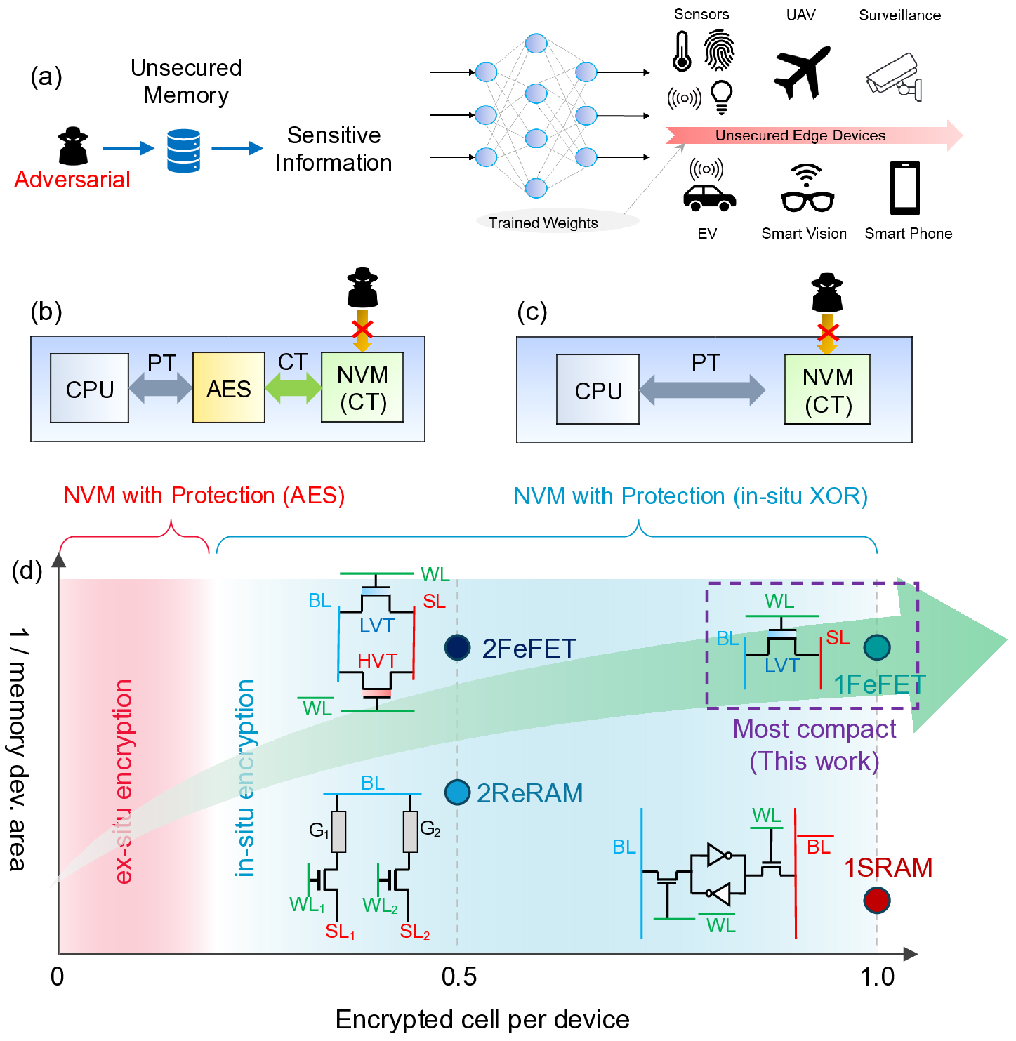
Prior lightweight implementations of FeFET-based XOR security schemes [19,21,20] employ pairs of complementary FeFET devices to implement the XOR cipher. In these designs, each ciphertext bit is encoded by two FeFETs with opposite polarization states, storing one encrypted bit across a complementary device pair and thereby doubling the required memoryarray capacity relative to conventional unencrypted storage. Xu et al. [19] demonstrate an AND-type memory array using two FeFETs per unit cell, where the transistors are con-nected in parallel at their source-drain terminals and designed with complementary thresholds (Fig. 2b). Because decryption keys are applied through the shared wordline, decrypting a fine-grained key-protected block requires two wordline activations (two cycles) per row. Shao et al [21] extends complementary-cipher storage to support in-memory multiply-accumulate (MAC) on encrypted weights. Zijian et al. [20] adopt the XOR-cipher technique for vertical NAND FeFETs in which the ciphertext is stored as the configuration of two cells, and decryption is performed by applying key-dependent read wordline biases to two pages simultaneously-likewise doubling storage capacity and requiring two read cycles for fine-grained key-encrypted block decryption.
So far, all reported in-situ XOR schemes incur a 100% area penalty to achieve security.
The most desirable approach would therefore be to embed security directly within the memory array without sacrificing effective memory density-that is, to realize an in-situ XOR operation using a single memory device. Although several studies have explored in-memory XOR logic using a single memory element, these efforts have not been pursued in the encryption context [32,33]. For example, Reis et al. [33] introduced a word-level in-memory XOR architecture in which both inputs are stored using a 2T+1FeFET configuration per memory bit, and the XOR operation is resolved through complex sense-amplifier circuitry. Although this approach employs only one memory device, each cell effectively involves three devices, which remains far from the goal of an ultimate single-device design. Separately, Chakraborty et al. [32] demonstrated a single-transistor XOR gate based on an FDSOI FeFET, utilizing a fundamentally different mechanism. In their design, two inputs are applied sequentially across the device terminals (gate, source, and drain), and a drain-erase-assisted programming sequence encodes the XOR result into the final V TH state. However, realizing this function requires multiple write/inhibit steps to traverse successive threshold levels, leading to significant latency and energy overheads.
Given these challenges, we propose, for the first time, an ultra-compact in-situ XOR operation using a single memory device, enabling encryption without any density penalty.
As illustrated in Fig. 1d, a single FeFET functions as an encrypted cell by directly storing the ciphertext. The density advantage is achieved through a novel in-memory XOR-based decryption mechanism that operates without complementary storage. Leveraging the threeterminal nature of FeFETs, the proposed compact cryptographic memory primitive employs a source/drain current-direction key-decoding scheme to enable single-cycle decryption, while the FeFET’s V TH states directly store encrypted data. This approach eliminates the need for auxiliary complementary bit storage required in prior lightweight XOR-based schemes, paving the way toward an extremely compact memory architecture that seamlessly integrates storage and security functionalities within a single device. Moreover, since the decryption key is no longer distributed through a shared horizontal wordline, the design supports finegrained, device-level decryption within a single cycle. Finally, we demonstrate that the scheme naturally extends to exploit the multilevel-cell (MLC) capability of FeFETs, enabling multiple encrypted bits to be stored per device-further reducing the encrypted array footprint and advancing bit-density scaling. Also, our proposed scheme can be extended to other 1T-1R memories as well.
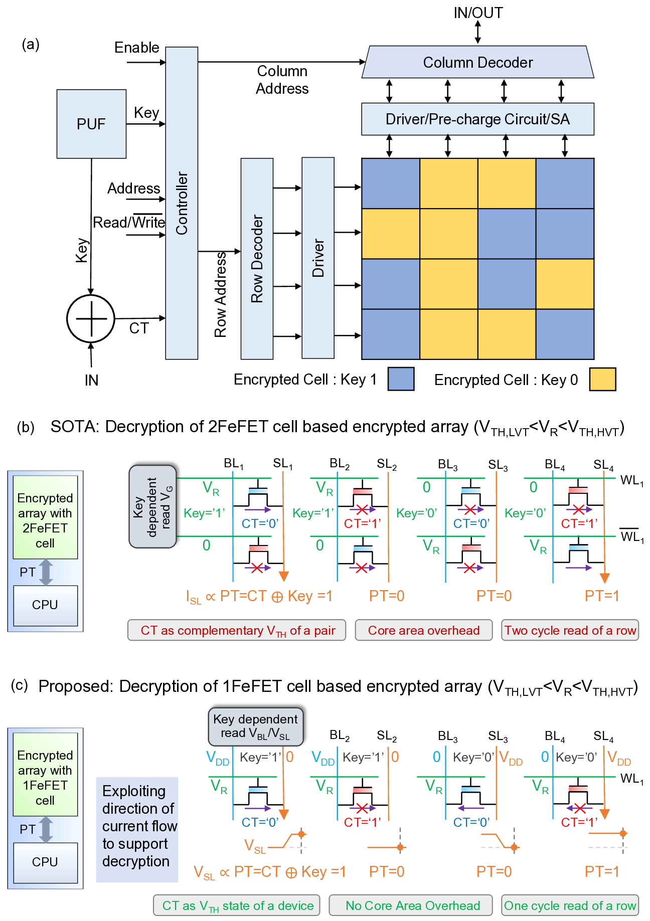
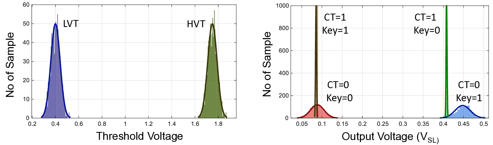
Overview of the proposed in-memory encryption/decryption scheme Fig. 2(a) provides an overview of the proposed in situ XOR-based encryption/decryption scheme integrated with the FeFET memory array and its associated peripheral circuitry. In plaintext (unencrypted) operation, a single FeFET cell stores one bit (0/1); accordingly, each cell is programmed to a low-or high-threshold voltage state (LVT/HVT) depending on the data value. In our encrypted design, each cell is protected with a 1-bit key without any storage overhead, preserving ultra-dense memory (one encrypted bit per cell). For 1-bit encrypted storage, each cell is programmed to either HVT or LVT, with the FeFET driven to the desired state by applying write pulses of ±V W ( Fig. S3). In our scheme, keys do not need to be shared across a row, enabling fine-grained per-cell encryption; successive cells can be encrypted with key 0 or key 1 without performance degradation. XOR designs use a two-transistor (2T) cell that stores complementary bits. This structure requires two decryption (read) cycles, with the key bit (0/1) applied on the same row [19].
(c) Proposed 1T FeFET XOR scheme: the ciphertext is encoded in a single transistor by programming the device threshold state (HVT/LVT). Decryption is performed by applying the key as a source-drain (S/D) bias; the plaintext bit is obtained by sensing the source node, which resolves high or low depending on the S/D current direction. Different keys (0/1) can be applied in parallel across a row within the same cycle.
Prior in-situ FeFET encryption [19] required two transistors per ciphertext bit (Fig. 2(b)).
Each ciphertext bit was encoded in a complementary FeFET pair where one FeFET is programmed to HVT and the other one programmed to LVT or vice versa. Decryption recovered the plaintext by sensing the sense-line current I SL while applying complementary read voltages (V R , 0) to the two gates. The key bit selects which transistor’s gate receives V R and which receives 0; depending on the HVT/LVT assignment and the applied key, the sensed current resolves to a logical high or low, revealing the plaintext bit. Using a two-FeFET (2T/bit) unit cell doubles the encrypted area and-when bits within a row use different keys-requires two read cycles per row because the row’s gate lines are shared and the key pair (V R , 0) is broadcast per row, increasing decryption latency.
In contrast, our proposed in-memory encryption stores each encrypted bit in a single
FeFET cell, preserving an ultra-dense encrypted array (1T/bit). During encryption, the ciphertext CT is generated by XORing the plaintext P T with the key Key : CT = P T ⊕Key .
When Key = 0, CT = P T (plaintext 0/1 maps to ciphertext 0/1); when Key = 1, CT = P T (plaintext 0/1 maps to ciphertext 1/0). We encode CT = 0 as a low-threshold (LVT) state and CT = 1 as a high-threshold (HVT) state in the FeFET cell, as illustrated in Fig. 2(c).
Decryption recovers the plaintext by XORing the ciphertext with the key, P T = CT ⊕ Key .
We realize this XOR in a single-transistor, single-cycle read by treating the FeFET’s V TH state as one operand (i.e., CT) and the BL/SL polarity as the other (i.e., decryption key).
The key is encoded in the drain-/source-line biases. For Key = 1, initialize V SL = 0 (GND) and bias V BL = V DD ; for Key = 0, precharge V SL = V DD and tie V BL = 0 (GND). A read pulse V R is applied on the word line (WL) with LV T < V R < HV T , so an LVT cell (CT = 0) turns on while an HVT cell (CT = 1) remains off. The plaintext is the final voltage on the source line (SL) after the read: if SL resolves to V DD , then P T = 1; if SL resolves to GND, then P T = 0. Intuitively, when CT = 0 (LVT), the channel conducts and SL is driven toward BL, yielding P T = BL = Key ; when CT = 1 (HVT), the channel is off and SL holds its precharge, yielding P T = SL init = Key . Thus the operation implements P T = CT ⊕ Key in one cycle.
Fig. 2(c) summarizes the four decryption combinations of a 1-bit ciphertext and 1-bit key.
For Key = 1, CT = 0 (i.e., Key ⊕CT = 1⊕0), the ciphertext maps to a LVT FeFET. A key of ‘1’ sets SL = 0 (GND) and BL = 1 (V DD ). When the wordline (WL) is driven by the read voltage V R , chosen such that LVT < V R < HVT, the SL potential rises toward V DD , yielding P T = 1. For Key = 1, CT = 1 (1⊕1), the ciphertext corresponds to a high-threshold (HVT)
FeFET. With SL = 0 and BL = 1, the channel remains off at V R , the SL remains at GND, and P T = 0. For Key = 0, CT = 0 (0 ⊕ 0), the ciphertext corresponds to LVT. The key ‘0’
precharges SL = 1 (VDD) and sets BL = 0 (GND). When WL is pulsed to V R , the device conducts, pulling SL down to GND and producing P T = 0.For Key = 0, CT = 1 (0 ⊕ 1), the ciphertext corresponds to HVT. With SL = 1 and BL = 0, the device remains off at V R ;
SL stays near V DD , yielding P T = 1.These outcomes are consistent with P T = CT ⊕ Key .
Also note that, because the decryption keys are applied to the vertically routed SL and BL lines in the memory, keys do not need to be shared across a row(Refer Fig. S2). This enables fine-grained per-cell decryption: cells in the same row can use key 0 or key 1 independently, allowing row-wide decryption in a single cycle. Simulation verification is given in Fig. S4.
Threshold variation analysis in Fig. S6 shows that the PT0/PT1 states are distinguishable with the proposed scheme.
Fig. 2(a) represents an overview of the proposed in situ XOR-based encryption / decryption scheme with FeFET memory array. We integrate a PUF-derived key [34] with the memory array to generate unique encryption keys for each device. For 1-bit encrypted storage, each cell is programmed to either a high-or low-threshold state (HVT or LVT) through coordinated control of the row decoder, column decoder, and driver circuits. Instead of us-ing a shared key across a row, a fine-granularity encryption scheme is implemented. The ciphertext bit is generated by XORing the input plaintext with the key derived from physically unclonable function (PUF). During decryption, appropriate biases are applied through the wordline (WL), bitline (BL), and sourceline (SL) using the decoders, drivers and pre-charge circuitry, The sense amplifier (SA) detects the SL voltage to decrypt the binary plaintext.
Unique encryption keys for the memory array can be realized by deriving them from a PUF implemented in the memory array itself [34]. A PUF is a hardware-security primitive that exploits innate physical variations of a device [35] to generate unique and non-replicable keys. NVM elements are particularly well suited for PUF implementation, since their internal operating mechanisms naturally produce random responses even under identical external stimuli. For example, FeFET-based NVMs exhibit stochastic polarization switching under identical programming pulses, which results in random variations in drain current [14,36].
Such stochastic switching behavior of the ferroelectric layer inherently yields distinct keys for every device. FeFET-based PUFs have been implemented in both single-and dual-transistor configurations [34]. To reduce key volume and simplify key management, block-cipher-based encryption can be adopted instead of fine-grained per-cell encryption. In this scheme, each memory block is encrypted using a unique key, ensuring that different blocks are still protected by distinct keys.
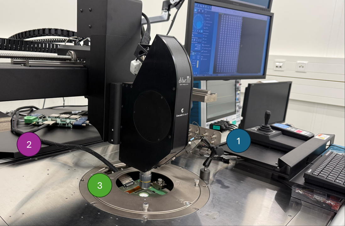
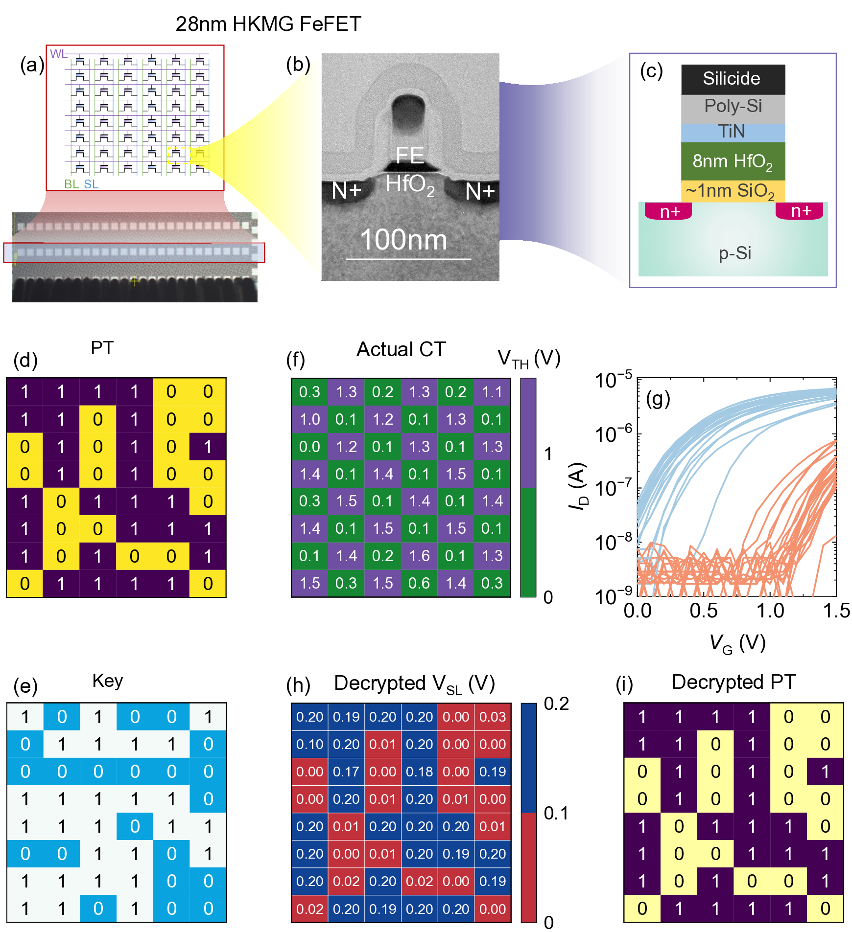
Next we show the experimental validation of the proposed encryption/decryption scheme shown in Fig. 2 using a FeFET AND array implemented on GlobalFoundries’ 28nm high-κ metal gate (HKMG) platform [37]. In this work, an 8x6 FeFET AND array is adopted for proof of concept, as shown in Fig. 3(a). On-wafer probe card testing system is adopted for the array testing, as shown in Fig. S1. The top-view optical image of the array shows the needles to contact pads and a total of 25 pads are used for this array. Detailed device information and processes can be found in [37]. The cross-sectional transmission electron microscopy (TEM) of the FeFET is shown in Fig. 3(b), where the gate stack features a 8nm thick doped HfO as the dielectric (per Fig. 3(c)), rather than the high-κ dielectric in the logic device. Except for the gate dielectric difference, the FeFETs share the same processing as the logic device, and thus can be integrated side-by-side with logic device, making it versatile for various applications.
The proposed scheme can also be extended to multi-level-cell (MLC) operation, enabling higher storage density while maintaining the same number of storage devices. Partial polarization states in the ferroelectric layer of FeFETs give rise to multiple distinct, nonvolatile V TH levels, which can be exploited to realize MLC storage. In this section, the
For 2-bit decryption, the plaintext is decoded from the sequence of sense-line (SL) outputs obtained during three FeFET read cycles. In these three cycles, the word line (WL) is biased sequentially with the read voltages V R2 , V R1 , and V R3 , which are chosen such that The decryption key bits are applied as bias voltages on the BL/SL lines. For a key bit of 1, the BL is biased at V DD while the SL is pre-charged to 0 V (BL/SL = 1/0), as illustrated in Fig. 4(d). For a key bit of 0, the BL is biased at 0 V and the SL is pre-charged to V DD (BL/SL = 0/1).
PT coded with SL output sequences during 3 cycles’ read
Cycle 1 for decryption of MSB @CT_MSB=0, Cycle 2 for decryption LSB @CT_MSB=1, Cycle 3 for decryption LSB In the first read cycle, with V R2 applied to the WL, the most significant bit of the plaintext, P T MSB , is extracted. First consider the case Key MSB = 1, implemented by BL/SL = 1/0 (V BL = V DD , V SL precharged to 0 V).For cells programmed to CT ‘00’ or CT ‘01’ (i.e., with V TH,00 or V TH,01 ), V R2 is larger than the threshold voltage, the FeFET turns on, and V SL is driven toward V DD . This SL level is decoded as P T MSB = 1. For cells programmed to CT ‘10’
or CT ‘11’ (with V TH,10 or V TH,11 ), V R2 is below the threshold voltage, the FeFET remains off, and V SL stays near 0 V, which is decoded as P T MSB = 0. Similarly, for Key MSB = 0, realized by BL/SL = 0/1 (V BL = 0 V, V SL precharged to V DD ), cells with CT ‘00’ or CT ‘01’ (low-V TH states) turn on and discharge SL from V DD to 0 V, yielding P T MSB = 0, whereas cells with CT ‘10’ or CT ‘11’ (high-V TH states) leave SL at V DD , yielding P T MSB = 1. Thus, in all cases the extracted P T MSB satisfies CT MSB = Key MSB ⊕ P T MSB .
When CT MSB is 0 (CT = ‘00 ′ / ′ 01 ′ ), then we read out the LSB plaintext from SL voltage during second cycle with V R1 on WL. If Key LSB = 0(BL/SL = 0/1), V SL would be driven to GND for CT ‘00’, indicating the value for P T LSB to be 0. However, V SL stays at V DD for CT ‘01’, indicating the value for P T LSB is 1. In contrast, if the key LSB is 1 (BL/SL=1/0),
V SL is driven to V DD for CT ‘00’, inferring P T LSB to be 1. For CT ‘01’, V SL stays at GND, which indicates the value for P T LSB is 0. However, if CT MSB is 1 (CT = ‘10 ′ / ′ 11 ′ ), then we read out the LSB plaintext from SL voltage during third cycle with V R3 on WL. If Key LSB = 0(BL/SL = 0/1), V SL would be driven to GND for CT ‘10’, indicating the value for P T LSB to be 0. However, V SL stays at V DD for CT ‘11’, indicating the value for P T LSB is 1. In contrast, if the key LSB is 1 (BL/SL=1/0), V SL is driven to V DD for CT ‘10’, inferring P T LSB to be 1 while V SL stays at GND for CT of ‘11’ and Key LSB of 1 (BL/SL=1/0), which indicates the value for P T LSB is 0. Simulation verification is shown in Fig. S5. such encoding errors can be avoided in existing flash memory and also FeFET with a large memory window designed for storage applications [38]. In this work, we focus on validating the encryption/decryption principles and leaving the device optimization for the future re-search.
During decryption, voltages are applied according to the key matrix in Fig. 4(h), and the resulting SL voltages are mapped to the decrypted plaintext matrix in Fig. 4(m). A decryption error rate of 3 out of 48 cells is observed, as illustrated in Fig. 4(n). Out of the three decryption errors, two of them correspond to encryption failures, which can be fixed by write scheme on appropriate devices. Meanwhile, one encryption error disappears during decryption, and a new decryption error appears. For the device at column 5, row 7, its actual V TH is around 0.8 V, which lies between data states 1 and 2. This overlap may have caused the encryption error. However, its current at V R2 is close to that of data 1, so the error disappears during decryption. For the device at row 6, column 2, although the data are correctly encrypted, the current at V R2 is quite low, leading to a decryption
We compare the proposed FeFET in-memory XOR encryption/decryption with (i) an AESbased scheme [39] and (ii) a prior FeFET-based encryption design [19]. The comparison spans area, latency, power, and throughput (Fig. 5). The analysis is performed for an encrypted memory array clocked at 25 MHz (40 ns cycle), aligned with previous AES work [39]. We target an 128×128 plaintext memory array to be encrypted. In this work, the encrypted FeFET memory uses a 128×128 array, whereas the prior work uses a 256×128 array. The design employs sixteen sense amplifiers (SAs) to decrypt one 128-bit row; each SA is time-multiplexed across eight columns (one column per cycle), so a full-row decrypt completes in eight cycles. Our design achieves substantially lower area than prior works, as illustrated in Fig. 5(a). Earlier AES-based approaches report an area of 0.00309 mm 2 [39], while both the prior FeFET design and our scheme incur negligible overhead comparing to the whole memory area cost as this scheme needs only some XOR gates used to generate ciphertext [19].
Importantly, the core array in our scheme introduces zero transistor overhead: the encrypted array uses the same number of devices as the plaintext array. In contrast, the prior FeFET in-memory encryption design doubles the device count (e.g., 256×128 FeFETs) relative to an equivalently sized plaintext array, whereas our encrypted array for a 128 × 128 configuration preserves the original device count [19]. Based on layout analysis given in Fig. S7, the area per 1-bit ciphertext in our design is reduced by 50% compared to the previous FeFET-based approach [19], as shown in Fig. 5(d), resulting in significant reduction in the core array area. AES accelerator [39], the prior FeFET-based design [19], and this work. Our design achieves encryption/decryption throughput that is 45.2×/14.12× higher than AES and 2×/2× higher than the prior FeFET design. (b) Performance comparison of AES (Weiwei Shan et al. [39]), the prior FeFET scheme (Yixin Xu et al. [19]), and this work across seven neural-network workloads, showing an average total latency reduction of 95% relative to AES, and (c) Total latency reduction of 50% compared with the previous FeFET-based scheme. (d) Encrypted cell area reduction of 50% compared with the prior FeFET work.
The proposed design demonstrates significant latency and throughput improvements over prior works. The array operates at 25 MHz (40 ns clock period), consistent with the AES work [39]. Our scheme uses a fixed 100 ns write window per 128-bit row, corresponding to 2.5 encryption cycles (100 ns / 40 ns = 2.5). In our work, decryption takes one cycle per bit for both key values (0/1), enabling single-cycle, fine-grained decryption across the row.
With sixteen sense amplifiers (SAs), the 128-bit word is partitioned into eight parts, so a full-row decrypt completes in eight cycles. Thus, our latency for a 128-bit row is (encryption, decryption) = (2.5, 8) cycles. For 128-bit data using AES, the latency is (115.5, 121) cycles [19], so our work achieves encryption/decryption latency improvements of 46.2×/15.13× over AES. Prior FeFET work uses 2 FeFETs per 1-bit ciphertext; therefore, it requires two write cycles for encryption. For decryption, two read cycles are also required due to wordline/key sharing (keys applied via wordlines) across rows, which prevents simultaneous fine-grained decryption. Its latency is (5,16) cycles (encryption/decryption), i.e., 2×/2× higher than ours. One approach to further improve decryption latency/throughput would be to increase the number of SAs. We also evaluate throughput at a 25 MHz clock frequency. Encrypting 128-bit data takes 2.5 cycles (100 ns), yielding 1,280 Mbps encryption throughput. With 16 SAs, decryption processes 16 bits per cycle (40 ns), yielding 400 Mbps decryption throughput.
The (encryption, decryption) throughput for AES is (28.32 Mbps, 28.32 Mbps) [39], and for the prior FeFET design is (640 Mbps, 200 Mbps). Note, in this analysis, we assume the case of different key bits applied in the same row. Therefore, our design achieves 45.2×/14.12× higher throughput than AES and 2×/2× higher than the prior FeFET design.
Next we show how the array level performance is impacting the system level performance.
To compare the impact of encryption/decryption latency across diverse neural-network workloads, we conduct a case study on AlexNet, MobileNet, Faster RCNN, GoogleNet, ResNet-18, YOLO-Tiny, and DLRM. We evaluate three schemes: a conventional AES baseline [39], a prior FeFET-based design [19], and our proposed approach. Experiments are performed with SCALE-Sim [40,41], a widely used simulator for systolic CNN accelerators. All workloads execute on a TPU-like systolic array (weight-stationary dataflow). In our design, encrypted weights (ciphertext) reside in a 1T-FeFET memory array and are decrypted and provided as plaintext to the systolic array, which processes each layer under a weight-stationary dataflow.
The computation outputs are then read, encrypted, and stored back to the FeFET array.
Using SCALE-Sim, we obtain workload-specific reads and writes to the memory array. Our analysis shows that the encryption and decryption latency overhead is significantly reduced with our proposed in-situ encryption/decryption. Our scheme achieves an average latency reduction of 95% compared to AES, as shown in Fig. 5(b). Relative to the prior FeFET-based design, our approach delivers an 50% latency reduction as shown in Fig. 5(c), enabled by two architectural advantages: (i) one-bit-per-transistor (1T-FeFET) encoding and (ii) parallel application of decryption key bits (0/1) in a single read cycle. By contrast, the prior FeFET scheme uses two FeFETs per bit and requires two read cycles for fine-grained decryption, resulting in higher latency and reduced efficiency.
To summarize this work, we propose a XOR-based in-memory hardware-based encryption scheme. We use only one transistor for an unit cell, which makes the design ultra compact.
We verify the functionality of the proposed design through software simulation and fabrication data. We also conduct a case-study on different neural network workloads to compare the performance benefit of the proposed design against state-of-the-art work. In ours, the individual keys are applied simultaneously which halves the decryption latency than the stateof-the-art work.
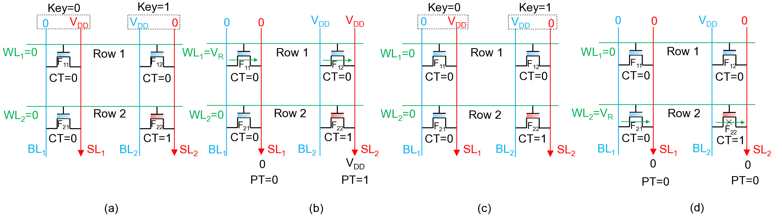
In the 1-bit FeFET encrypted memory array shown in Fig. S2, decryption of one row of ciphertext (CT) can be completed in a single cycle. The memory array shares the wordline (WL) along each row, while both the bitline (BL) and sourceline (SL) are shared along each column. Fine-grained keys are applied as bias voltages on the vertical BL/SL lines, whereas the read voltage V R is applied to the shared WL of the selected row. Consequently, both key values (0 and 1) can be applied in parallel across different columns in this array architecture.
In contrast, prior work [19] applies the key through shared WL lines and therefore requires two decryption cycles per row. Fig. S2(a-d) illustrates plaintext (PT) recovery in a 2 × 2 array of ciphertexts with a column-wise key set of (0, 1). Row 1 stores the ciphertext (0, 0), which corresponds to the device configuration (LVT, LVT). As shown in Fig. S2(a), to apply key = 0 to the first ciphertext column, the bias (BL 1 /SL 1 ) = (GND/V DD ) is applied. Similarly, to apply key = 1 to the second ciphertext column, the bias (BL 2 /SL 2 ) = (V DD /GND) is used. When V R is asserted on W L 1 , both FeFETs in Row 1 are LVT devices; thus, both SL lines are driven to the voltage level supplied at their respective BLs, as shown in Fig. S2(b). Specifically, SL 1 is pulled to GND and SL 2 is pulled to V DD , yielding plaintext (0, 1), consistent with the XOR relation P T = Key ⊕ CT , i.e., Key = (0, 1) and CT = (0, 0). Fig. S2(c) shows the application of the same column-wise key pattern (0, 1) to the stored ciphertext (0, 1) in Row 2, which corresponds to the device configuration (LVT, HVT). In this case, when V R is applied to WL2, SL 1 is driven to GND because the corresponding FeFET is LVT.
However, the FeFET in the second column is HVT, so SL 2 remains at GND. As a result, the final SL voltages for the two columns are (GND, GND), which translates to plaintext (0, 0). This outcome again matches the XOR logic P T = Key ⊕ CT , with Key = (0, 1) and CT = (0, 1). Sensed SL voltages corresponding to PT = (0, 0).
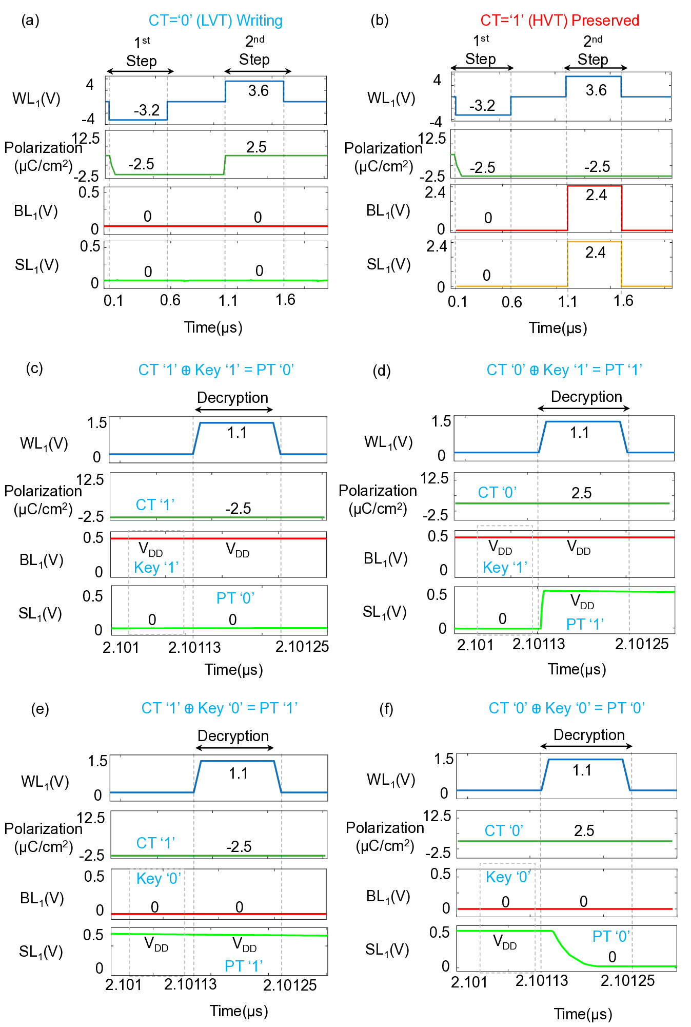
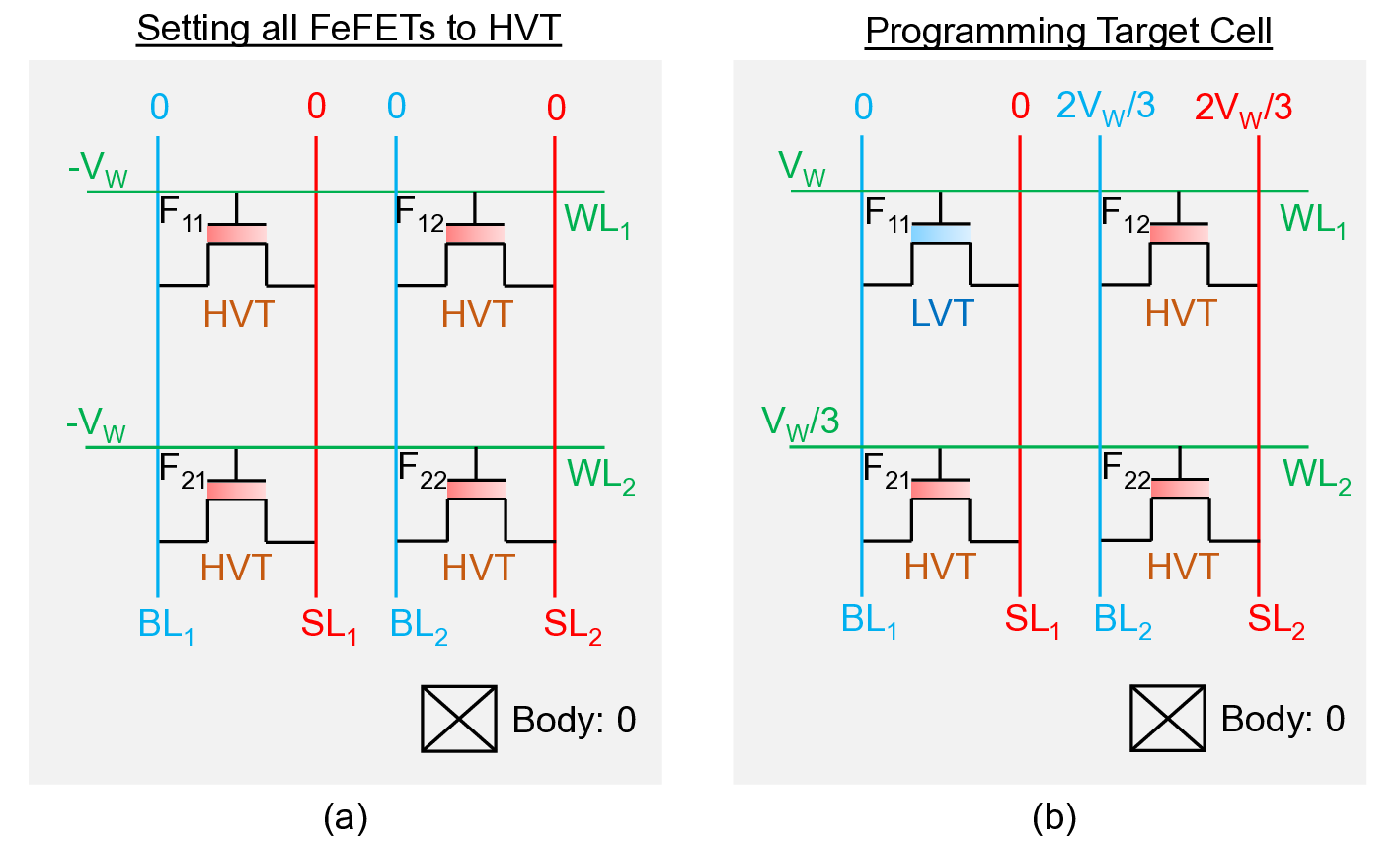
The FeFET array writing is illustrated in Fig. S3. The target array state is CT = (0,1) in the first row, corresponding to (LVT, HVT). FeFETs in a row are written using a two-step procedure following the V W /3 scheme [42]. In the first cycle, all cells are initialized to HVT by applying -V W to each WL. In the second cycle, the target FeFET F Simulation and analysis are performed in the Cadence Virtuoso ADE-XL Spectre environment using the open-source NCSU 45 nm Basekit [43] together with a multi-domain FeFET compact model [44]. The functionality of the proposed design is verified and discussed in detail in this section based on the array structure demonstrated in Fig. S2. Fig. S4 illustrates the transient simulation results for encrypted FeFET cell programming (refer Fig. S3). The programming of ciphertext logic ‘0’ and ‘1’ is shown in Fig. S4(a) and Fig. S4(b), respectively. A negative gate bias of 3.2 V (-V W ) is applied to reset the FeFET polarization to -2.5 µC/cm 2 (HVT), whereas a positive gate bias of 3.6 V (+V W ) sets the polarization to 2.5 µC/cm 2 (LVT), with both drain and source terminals grounded. A V W /3 write scheme is adopted to prevent unselected cells from switching their polarization states [42]. During the second step of the programming operation, unselected BL and SL lines are biased at 2.4 V (+2V W /3), while all unselected WL lines are biased at 1.2 V (+V W /3). This biasing condition preserves the polarization state of unselected cells even when the programming pulse is applied to the selected row. Fig. S4(c-f) covers the decryption process of all 4 possible combinations of 1-bit ciphertext and key. After the SL is precharged and the appropriate key-dependent bias voltage is applied to the BL, the plaintext data are observed at the SL when a read voltage V R is applied to the WL, with V LVT < V R < V HVT . A read voltage of V R = 1.1 V is chosen, which enables approximately 98% drain-to-source voltage transfer when the FeFET is in the LVT state.
Figure S4(c) illustrates decryption of ciphertext CT = 1 (HVT) using key = 1 with BL/SL = (V DD / GND) and V DD = 0.5 V. When V R is applied to the WL, the SL remains at ground, corresponding to plaintext PT = 0. Figure S4(d) shows decryption of ciphertext CT = 0 (LVT) using the same key = 1 and BL/SL = (V DD / GND). In this case, when V R is applied to the WL, the SL rises close to V DD through the conducting LVT FeFET, indicating plaintext PT = 1. Figure S4(e) demonstrates decryption of ciphertext CT = 1 (HVT) using key = 0 with BL/SL = (GND/ V DD ). Upon application of V R to the WL, the HVT FeFET remains off, so the SL stays at V DD corresponding to plaintext PT = 1. As shown in Figure S4(f), decryption of ciphertext CT = 0 (LVT) with key = 0 and BL/SL = (GND/ V DD ) causes the SL to be discharged to ground when V R is applied to the WL, indicating plaintext PT = 0. are selected for CT = 00, 01, 10, and 11, respectively. In the first read step, BL and SL are biased according to Key MSB , and the WL is driven with 1.8 V (V R2 ). The resulting SL voltage is sensed to determine PT MSB . In the second read step, Key LSB is applied to the BL and SL, and a read pulse of 1.1 V (V R1 ) is applied to the WL. The BL and SL are then rebiased with Key LSB , and a third read pulse of 2.5 V (V R3 ) is applied to the WL in the third step.
Depending on CT MSB , the SL voltage in either the second or third cycle determines PT LSB .
Figure S5(a) shows decryption when (CT, Key) = (11,11). The level CT = 11 corresponds to the highest threshold voltage and therefore does not conduct for any of the three read pulses. For Key = 11, the BL/SL pair is biased as (V DD , GND) in all three cycles, so the recovered plaintext is PT = 00. Figure S5(b) shows decryption when (CT, Key) = (00, 00).
The level CT = 00 has the lowest threshold voltage and conducts for all three read pulses.
With Key = 00, the BL/SL pair is biased as (GND, V DD ) in each cycle, causing the SL to be pulled to GND every time, and the plaintext is decoded as PT = 00. Figure S5(c) illustrates decryption for (CT, Key) = (10, 01). The MSB of Key = 01 is encoded as BL/SL = (GND, V DD ) in the first step. The threshold voltage associated with CT = 10 is such that the FeFET turns on only when the highest read voltage V R3 is applied; consequently, it does not conduct in the first step when the WL is driven with 1.8 V, and the SL remains close to V DD . The LSB of Key = 01 is encoded as BL/SL = (V DD , GND) in the second and third cycles. For CT = 10, the second cycle is irrelevant. In the third cycle, when V R3 = 2.5 V is applied to the WL, the FeFET conducts and the SL is driven close to V DD .
Overall, this sequence decodes the plaintext as PT = 11. Figure S5(d) considers CT = 01, which corresponds to the second-lowest threshold voltage, and Key = 11. In all cycles, the BL/SL pair is biased as (V DD , GND). In the first cycle, the applied read voltage causes the FeFET to conduct and the SL to rise close to V DD . In the second cycle, when the WL is driven with V R1 = 1.1 V, the threshold voltage is higher than V R1 , so the FeFET is off and the SL remains at GND. The combination of SL levels across the read cycles corresponds to a decoded plaintext of PT = 10.
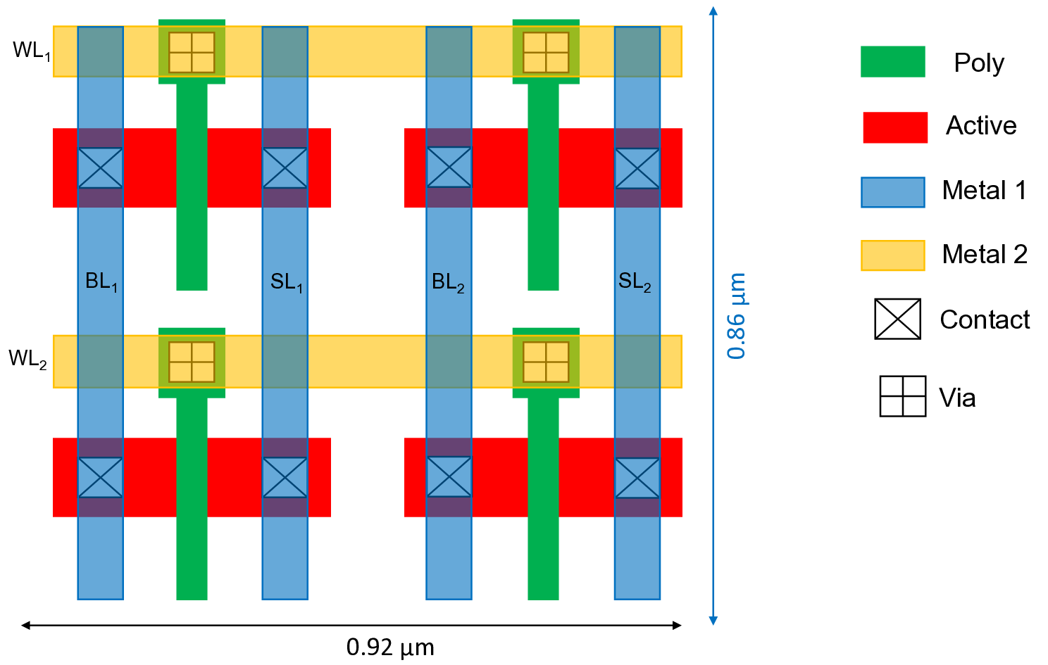
Fig. S7 shows the layout of the 2 × 2 array of the proposed 1T-encryption. For design GPDK045 rules [45] has been used. The area footprint of the 2 × 2 array is 0.7912 µm 2 for 45nm technology node.
📸 Image Gallery