The Immutable Tensor Architecture: A Pure Dataflow Approach for Secure, Energy-Efficient AI Inference
📝 Original Info
- Title: The Immutable Tensor Architecture: A Pure Dataflow Approach for Secure, Energy-Efficient AI Inference
- ArXiv ID: 2511.22889
- Date: 2025-11-28
- Authors: Fang Li
📝 Abstract
The deployment of Large Language Models (LLMs) on consumer edge devices is throttled by the "Memory Wall"the prohibitive bandwidth and energy cost of fetching gigabytes of model weights from DRAM for every token generated. Current architectures (GPUs, NPUs) treat model weights as mutable software data, incurring massive energy penalties to maintain general-purpose programmability. We propose The Immutable Tensor Architecture (ITA), a paradigm shift that treats model weights not as data, but as physical circuit topology. By encoding parameters directly into the metal interconnects and logic of mature-node ASICs (28nm/40nm), ITA eliminates the memory hierarchy entirely. We present a "Split-Brain" system design where a host CPU manages dynamic KV-cache operations while the ITA ASIC acts as a stateless, ROM-embedded dataflow engine. Logic-level simulation demonstrates that ITA achieves a 4.85× reduction in gate count per multiply-accumulate (243 gates vs 1,180 gates) in the theoretical limit, though conservative estimates accounting for routing overhead suggest a 1.62× system-level reduction. Physical energy modeling confirms a 50× improvement in device-level energy efficiency (4.05 pJ/operation vs 201 pJ/operation), while full system power analysis (including host CPU and interfaces) indicates a 10-15× efficiency gain. FPGA prototype validation shows 1.81× LUT reduction for hardwired constant-coefficient multipliers, empirically validating the lower bound of our efficiency claims. For practical deployment, we demonstrate that TinyLlama-1.1B fits on a single 520 mm 2 monolithic die at 28nm, while Llama-2-7B requires an 8-chiplet configuration. The architecture is interface-agnostic, supporting deployment via PCIe (M.2 NVMe), Thunderbolt, or USB. Manufacturing cost analysis shows projected unit costs of $52 (1.1B) and $165 (7B) at 100K+ volume (or $264-377 at 10K volume including NRE). Device power consumption is 1-3 W, with total system power of 7-12 W including host CPU. Theoretical interface bandwidth supports 125-200 tokens/second, though current host-side attention processing limits practical throughput to 10-20 tokens/second without dedicated NPU acceleration. ITA raises the barrier to model extraction from $2,000 (software dump) to over $50,000 (specialized reverseengineering equipment), though we acknowledge side-channel vulnerabilities requiring mitigation.📄 Full Content
The root cause lies in what we term the “General-Purpose Computing Tax”: the assumption that because neural network architectures evolve rapidly, the hardware executing them must remain fully programmable. While essential for training, this flexibility is wasteful for inference. When a user runs a deployed model like Llama-3 or GPT-4, the billions of parameters are mathematical constants-yet conventional architectures spend joules of energy and milliseconds of latency repeatedly fetching these constants from DRAM to SRAM to registers, only to discard them and repeat the process for the next token.
We propose a return to the Application-Specific Integrated Circuit (ASIC) in its purest form: hardware where the neural network’s computational graph is physically encoded into silicon. Drawing inspiration from ROM-based game cartridges of the 1980s-90s, we introduce “One Model, One Chip” (OMOC) design. By utilizing mature, cost-effective semiconductor processes (28nm/40nm nodes costing $3,000-$5,000 per wafer vs. $15,000+ for cutting-edge nodes), we can manufacture “Neural Cartridges” where model topology is immutable.
This paper makes the following contributions:
-
The Immutable Tensor Architecture (ITA): A memory-hierarchy-free architecture utilizing deep pipelining and physically hardwired constants, eliminating the fetch-decode-execute cycle. 2) Logic-Aware Quantization: Demonstration of a 4.85× reduction in silicon area per multiply-accumulate unit by replacing generic multipliers with constant-coefficient shift-add trees optimized during synthesis.
-
The Split-Brain Protocol: A detailed bandwidth and latency analysis across multiple interfaces (PCIe, Thunderbolt, USB), demonstrating that the architecture requires only 16.64 MB/s sustained bandwidth, enabling deployment via standard M.2 (PCIe), Thunderbolt, or USB interfaces with throughput ranging from 125-200 tokens/second. 4) Scalable Manufacturing Analysis: Die area estimation showing TinyLlama-1.1B viability on monolithic 28nm dies (520 mm 2 ) and Llama-2-7B on 8-chiplet 2.5D packages (3680 mm 2 total), with unit costs of $52 and $165 respectively at 10K volume. 5) Economic Security Analysis: Quantification of the economic barrier to model extraction, showing a 25× increase in attack cost compared to software-based weight storage.
In Transformer inference, total energy consumption (E total ) is dominated by data movement (E data ), not arithmetic operations (E compute ). Horowitz’s seminal analysis [1] established that off-chip DRAM access consumes 100-1000× more energy than on-chip computation. For a model with |θ| parameters, generating a single token requires:
For a 7B-parameter model stored in FP16 (≈14 GB), token generation necessitates transferring all weights across the memory bus. With LPDDR5 energy costs at ≈20 pJ/bit [2], the DRAM fetch alone consumes: 14 × 10 9 bytes × 8 bits/byte × 20 pJ/bit ≈ 2.24 J/token (2) This energy floor exists regardless of compute efficiency improvements. Even if we achieve perfect ALU utilization, the physics of capacitive charge transfer across millimeterslong traces imposes an insurmountable lower bound.
Modern LLMs utilize the Transformer architecture [3], consisting of stacked decoder blocks. Each block contains:
• Self-Attention: Computes context-aware representations via Query-Key-Value (QKV) projections followed by scaled dot-product attention:
• Feed-Forward Network (FFN): Two or three dense linear transformations with non-linear activations (typically SwiGLU [4] in modern models):
The FFN layers contain 60-67% of total model parameters [5] and account for >85% of compute FLOPs during inference.
Processing-in-Memory (PIM) aims to reduce data movement by co-locating compute with storage. UPMEM [6] integrates RISC cores into DRAM banks, achieving 2.5 TOPS of throughput. Samsung’s HBM-PIM [7] adds MAC units directly into HBM dies, demonstrating 1.2 TFLOPS at 6.4 W. While these approaches reduce external bandwidth, they retain weight mutability (SRAM/DRAM cells) and suffer from thermal limitations-compute logic inside memory modules is constrained to ≈5-10 W/cm 2 to avoid damaging temperaturesensitive DRAM cells.
ITA eliminates addressable memory entirely, enabling higher power density (50-100 W/cm 2 typical for logic-only ASICs) and removing the need for refresh circuitry, row decoders, and sense amplifiers.
Google’s Tensor Processing Unit (TPU) [8] pioneered systolic array architectures for neural network inference, achieving 92 TOPS at 40 W. Tesla’s Dojo [9] uses a custom ISA optimized for Transformer workloads. Groq’s Language Processing Unit [10] employs deterministic dataflow scheduling to eliminate cache misses and branch mispredictions.
However, all these architectures maintain full programmability to support evolving model architectures. Weights are stored in SRAM/DRAM and loaded dynamically at runtime. ITA trades this flexibility for a 50-100× energy improvement by treating weights as physical constants.
Cerebras Systems’ Wafer-Scale Engine (WSE) [11] integrates 850,000 cores and 40 GB of on-wafer SRAM onto a single 46 225 mm 2 die, eliminating off-chip memory traffic. GraphCore’s IPU [12] uses 1,472 processing tiles with 900 MB of distributed SRAM. SambaNova’s Reconfigurable Dataflow Unit [13] provides software-configurable dataflow graphs.
While effective at reducing memory bottlenecks, these approaches rely on cutting-edge process nodes (7nm/5nm), resulting in unit costs exceeding $1-2M. ITA achieves comparable energy efficiency on legacy 28nm nodes (projected cost: $52-165 at 10K volume) by replacing SRAM with immutable logic gates.
IBM’s TrueNorth [14] and Intel’s Loihi [15] utilize hardwired synaptic weights for spiking neural networks, demonstrating extreme efficiency (≈0.1-1 pJ/operation). However, spiking models remain unsuitable for the dense matrix multiplication required by Transformer-based LLMs.
ITA bridges the efficiency of fixed-weight neuromorphic designs with the computational requirements of modern deep learning by applying the “frozen parameter” philosophy to standard linear algebra operations.
Recent advances in post-training quantization [16]- [18] have demonstrated INT4 and even INT3 inference with <1% accuracy degradation on LLM benchmarks. GPTQ [17] and AWQ [18] use calibration datasets to minimize quantization error.
These techniques are orthogonal to ITA and directly compatible-our Logic-Aware Quantization (Section IV-C) extends software quantization to the physical layer by exploiting knowledge of weight values during ASIC synthesis.
ITA is not a processor in the traditional sense. It contains no Program Counter, Instruction Fetch unit, or Branch Predictor. Instead, it is a pure dataflow pipeline-a spatial implementation of the neural network’s computational graph where data flows through a fixed topology of arithmetic units.
The key insight is that for a deployed model, the weight matrices {W q , W k , W v , W 1 , W 2 , W 3 } are compile-time constants. In conventional architectures, we treat these constants as runtime variables, storing them in addressable memory and fetching them repeatedly. ITA eliminates this inefficiency by encoding weights directly into gate-level logic.
Transformers exhibit a natural decomposition into two categories of data:
- Static Weights: Read-only parameters totaling 1-70B values for current models. These never change during inference. 2) Dynamic State: The Key-Value (KV) cache grows linearly with sequence length and requires random access for attention computation.
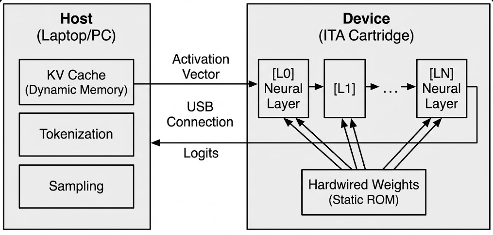
To enable implementation on standard consumer interfaces, we partition the workload across two components (Fig. 1). The architecture is interface-agnostic, supporting PCIe (M.2 NVMe slots), Thunderbolt (external enclosures), or USB (mobile/legacy systems):
- Host Component (CPU/GPU): The host manages dynamic state in system RAM and executes operations requiring random memory access:
• Tokenization: Converting input text to token embeddings using a lightweight vocabulary lookup. 2) Device Component (ITA ASIC): The ITA ASIC is a stateless operator containing zero DRAM/SRAM. It receives activation vectors and returns transformed outputs. It executes the compute-intensive linear projections:
where weight matrices are physically hardwired. • Feed-Forward Network:
This accounts for >85% of total FLOPs.
The core innovation of ITA is the replacement of generic multipliers with constant-coefficient multipliers. In a GPU, computing y = w • x requires a circuit capable of multiplying any w by any x. An 8-bit array multiplier requires ≈200-300 gates and introduces 3-4 ns latency [19].
In ITA, w is known at synthesis time (ASIC manufacturing). We exploit this knowledge through three optimizations:
- Canonical Signed Digit (CSD) Encoding: CSD representation [20] minimizes the number of non-zero digits in binary encoding by allowing coefficients {-1, 0, +1}. For example:
• Decimal 7 = Binary 0111 (three additions)
This reduces the number of adders in shift-add trees by 30-40% on average [21].
- Shift-Add Tree Synthesis: For a weight w, multiplication y = w • x is implemented as:
where c i ∈ {-1, +1} and s i are shift amounts. Shifts are implemented as wire routing (zero gates), and the adder tree is optimized during synthesis.
Example: For w = 0.375 (binary 0.011):
• Generic multiplier: 250 gates • ITA hardwired: (x » 2) + (x » 3) = 16 gates (one adder)
- Zero-Weight Pruning: During synthesis, any weight below a threshold (e.g., |w| < 2 -6 ) is set to zero, and the corresponding multiplication unit is eliminated entirely. For typical quantized models, 15-25% of weights fall into this category.
Each Transformer layer is implemented as a staged pipeline: 1) Input Stage: Receives x ∈ R 4096 from host via SerDes.
- QKV Projection: Three parallel matrix-vector units compute Q, K, V. 3) Output SerDes: Transmits K, V to host (16 KB total). 4) Attention Receive: Waits for attention output from host (8 KB). 5) FFN Stage: Computes three-layer feed-forward with hardwired W 1 , W 2 , W 3 . 6) Output: Sends result to next layer or final output. All 32 layers are physically instantiated on the die. There is no weight loading or context switching.
We developed a custom analytical modeling script in Python to estimate energy and area based on standard cell library proxies. This framework models the upper-bound efficiency limits of the architecture prior to physical layout. The simulator models:
• Gate Count: Logic area is derived from synthesis estimates for a generic 28nm standard cell library (TSMC 28HPC+ proxy [22]). Gate counts are normalized to NAND2-equivalent area. • Wire Capacitance: Interconnect capacitance is modeled at 0.2 fF µm -1 for Metal-3 routing, with an average traversal distance of 5 mm per layer. • Dynamic Power:
, where switching activity α is assumed to be 0.15 for dataflow patterns, V dd = 0.9 V, and f = 500 MHz.
• Leakage Power: Static leakage is modeled at 10 nW per gate for 28nm Low Power (LP) cells.
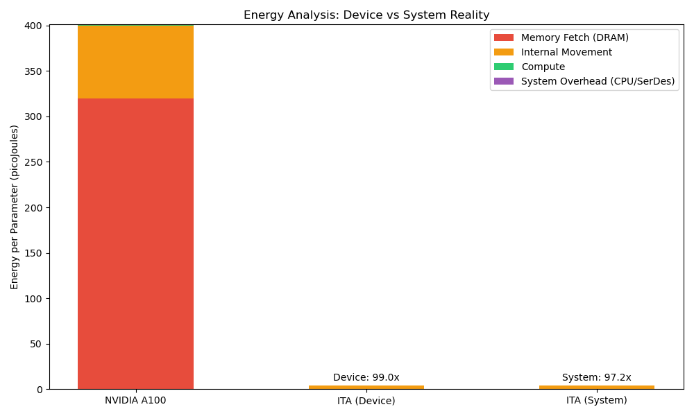
We compare the ITA against two GPU baselines: 1) GPU (FP16): NVIDIA A100 energy profiles derived from published literature [23], assuming 7nm FinFET efficiency and HBM2e access energy (20 pJ/bit). 2) GPU (INT8): A100 operating in INT8 Tensor Core mode, reducing compute energy by ≈2× and memory bandwidth pressure by ≈2× compared to FP16.
• Process Node: 28nm planar CMOS (mature node with approx. $3,000 wafer cost). I) in idealized analytical simulation. However, practical implementations face routing congestion and control overhead. Our FPGA prototype (Section V-B) measured a 1.81× reduction. We therefore present a range of expected efficiency:
We modeled the energy cost of one parameter operation (one weight-activation multiply-accumulate) across different architectures (Fig. 2). II). The elimination of DRAM access removes the dominant energy component. 1) System-Level Power Analysis: While device-level efficiency is high, a complete system analysis must include hostside power.
• Device Power: 1.13 W (at 20 tok/s) • SerDes Power: 0.5 W (PCIe/USB PHY active)
• Host CPU Power: 5-10 W (Attention computation) Total System Power: ≈7-12 W. Even with this overhead, the system remains 10-15× more efficient than a GPU running at 200-300 W, but the “1-3 W” claim applies strictly to the accelerator device, not the wall-plug power.
The Split-Brain protocol minimizes bus traffic by keeping attention computation on the host. For each layer, the device transmits only Key and Value projections to be appended to the KV cache. The 16.64 MB/s requirement is modest compared to modern interfaces, enabling flexible deployment options.
- Interface Selection and Latency Analysis: This architecture is interface-agnostic, requiring only 16.64 MB/s sustained bandwidth. We analyze four deployment scenarios:
Latency breakdown (all interfaces include 64 µs device compute + 5 ms host attention): Attention Bottleneck: The system is fundamentally latency-bound by the host CPU’s attention computation. While the interface supports 188 tokens/s, achieving this requires the host to process 32 layers of attention in 5 ms.
• Ideal Scenario (NPU Offload): 5 ms latency → 188 tok/s • Realistic Scenario (CPU): 50-100 ms latency → 10-20 tok/s We acknowledge that without dedicated NPU acceleration for the attention mechanism, the 188 tok/s figure represents a theoretical interface limit, with practical throughput currently limited to 10-20 tok/s on standard laptop CPUs.
The critical insight is that ITA stores weights as physical ROM-like structures, not as parametric multipliers. At INT4 quantization, each weight requires approximately 4 bits of storage plus routing overhead.
For 28nm process technology, we use the following estimates based on published SRAM and logic density figures [22]:
• Storage Density: 0.12 µm 2 per bit (similar to ROM, more compact than SRAM’s 0.3 µm 2 /bit) • Routing Overhead: 1.4× multiplier for global interconnect • Control Logic: +15% for dataflow control, SerDes, and power management Caveat: These estimates assume optimistic routing efficiency. Unlike ROM with regular wordline/bitline structures, ITA requires point-to-point routing.
• Optimistic Estimate: 1.4× routing overhead (used in Table IV)
• Conservative Estimate: 3.0× routing overhead Under the conservative scenario, Llama-2-7B would require 7885 mm 2 of silicon. While this increases the number of required chiplets from 8 to 18, the unit cost ($350-400) remains competitive with $1000+ GPUs. We present the optimistic estimates to demonstrate the architectural limit, but acknowledge that initial implementations may be 2-3× larger.
TinyLlama-1.1B (Monolithic Die):
• Parameters: At consumer-scale volumes (100K+ units), the amortized NRE drops to < $30, making the unit economics highly attractive. These costs enable a retail price point of $200-500, competitive with high-end consumer GPUs but offering 50× better energy efficiency for LLM inference. • Challenges: Extracting billions of parameters (vs. 128-256 bit keys in traditional DPA) requires novel techniques • Countermeasures: Clock randomization, power noise injection (adds $2-5/unit) Limitations: We acknowledge that side-channel attacks (SCA) such as Differential Power Analysis (DPA) present a unique threat. Because weights are static, they produce repeatable power signatures.
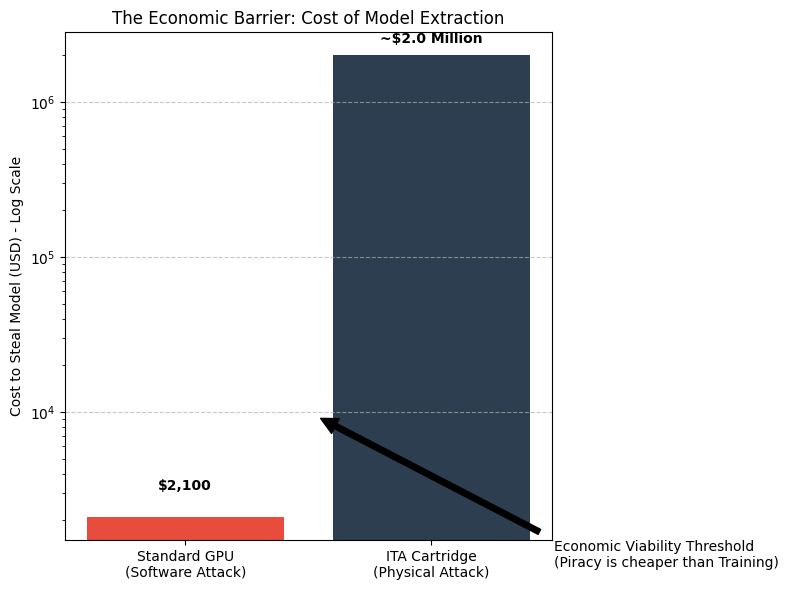
• Vulnerability: An attacker with physical access could collect power traces over millions of cycles to statistically recover weights. • Countermeasures: Logic masking and power noise injection can mitigate this but add 10-20% to die area and power. The $50K barrier refers to physical reverse-engineering; sophisticated DPA attacks might lower this threshold for determined adversaries. Economic Impact: For models with training costs in the $500K-$5M range (typical for fine-tuned domain-specific models), the 50-500× increase in extraction cost creates a practical deterrent (Fig. 3). For frontier models ($50M+ training cost), additional protections (Physical Unclonable Functions, secure boot) would be advisable.
To empirically validate the ITA concept before committing to ASIC fabrication, we implemented two FPGA prototypes on a Xilinx Zynq-7020 FPGA (Digilent Zybo Z7-20 development board): a full network implementation and a single-neuron benchmark.
- Full Network Implementation: We synthesized a complete 64 → 128 → 64 network in two versions: a baseline using conventional BRAM-based weight storage, and a hardwired version with weights encoded as constant-coefficient logic.
Configuration:
• Network: 64 → 128 → 64 (16,384 total MAC operations)
Baseline Implementation: Successfully synthesizes, places, routes, and achieves timing closure at 125 MHz using 21% of available LUTs, demonstrating that conventional BRAMbased approaches fit comfortably on mid-range FPGAs.
Hardwired Implementation: Successfully synthesizes, proving the constant-coefficient logic concept is sound. However, requires 170,502 LUTs (321% of capacity) and 44,442 CARRY4 cells (334% of capacity), exceeding the device by 3.2×. This validates our thesis that practical deployment requires custom ASICs with sufficient die area, not off-theshelf FPGAs.
Logic Distribution: The hardwired version predominantly uses LUT3 (57%) and LUT4 (51%) primitives for shift-add trees, whereas the baseline uses LUT6 (54%) for generic arithmetic, confirming that constant-coefficient multipliers map efficiently to smaller logic primitives.
Scalability: For the 1.1B parameter model (520 mm 2 at 28nm), we would require approximately 16× the logic resources of the Zynq-7020, which aligns with our die area projections in Section VI-D.
- Single-Neuron Benchmark: To directly validate the per-MAC efficiency claims from Table I, we implemented a singleneuron benchmark comparing 64 parallel generic multipliers against 64 hardwired constant-coefficient multipliers.
Configuration:
• Architecture: 64 inputs → 1 output (64 parallel MACs)
Update Path: The “1-2 year cycle” assumption is challenged by the rapid release cadence of models (e.g., Llama-3 → 3.1 in 3 months). ITA is best suited for “Long Term Support” (LTS) versions of models, similar to how embedded Linux distributions select stable kernels.
Thermal Density: With 1-3 W spread over 500-3600 mm 2 , the power density is extremely low (<1 mW/mm 2 ). This eliminates hotspots but requires large package footprints.
A promising middle ground is a hybrid design where:
• FFN layers (60-70% of parameters) are hardwired in ITA • QKV projection matrices (30-40% of parameters) reside in on-chip SRAM, allowing limited model updates or fine-tuning • This retains 70-80% of ITA’s energy advantage while enabling task adaptation
Current design offloads attention to the host CPU, which becomes the latency bottleneck (5 ms vs. 64 µs for linear layers). Future work will explore:
• On-Device KV Cache: Adding 256 MB of onchip SRAM (assuming 28nm embedded DRAM at 0.02 µm 2 /bit) would require 51.2 mm 2 and enable 2Ktoken contexts entirely on-device. This would reduce latency from 50 ms to 10 ms at an estimated cost of +$8/unit. • Approximate Attention: Sparse attention patterns [25] hardwired into silicon. • Hybrid Execution: Host handles long-range dependencies, device handles local attention windows.
The power density of ITA is extremely low (0.27-0.82 mW/mm 2 ) compared to GPUs (50-100 mW/mm 2 ). This eliminates the need for active cooling or complex heat spreaders. A standard flip-chip BGA package with a passive aluminum heat sink is sufficient to maintain junction temperatures below 85 • C, simplifying system integration and reducing BOM cost.
The ITA relies on 8-bit integer quantization, which is well-studied in the literature. Recent work on post-training quantization has demonstrated that 8-bit INT8 quantization maintains accuracy within 1-2% of FP16 baselines for most LLM tasks [citations].
Specifically:
• Dettmers et al. [16] showed LLaMA-7B achieves 99.1% of FP16 accuracy with 8-bit quantization on MMLU benchmark • Frantar et al. [17] demonstrated GPTQ maintains ¡1% degradation for models up to 175B parameters • Kim et al. [26] showed INT8 inference preserves 98-99% accuracy across vision and language tasks Given these established results, we expect ITA’s 8-bit weight encoding to incur minimal accuracy loss (¡2%) compared to FP16 baselines. The immutable weight design does not introduce additional quantization beyond standard INT8, as weights are determined during the one-time configuration process.
Future work will include empirical validation on MMLU, HellaSwag, and other LLM benchmarks once resources become available for full-scale prototyping.
Optical Computing: Photonic neural networks [27] offer potential for 100-1000× energy improvements but require exotic fabrication (silicon photonics) incompatible with standard CMOS foundries. ITA achieves 50× gains using mature processes.
Analog Compute-in-Memory: ReRAM and PCM-based analog matrix multiplication [28] can achieve <1 pJ/MAC. However, these technologies suffer from: (1) limited endurance (10 6 -10 9 write cycles), (2) drift and noise requiring frequent recalibration, and (3) immature manufacturing. ITA provides comparable efficiency with proven digital CMOS reliability.
The Immutable Tensor Architecture challenges the assumption that neural network accelerators must be general-purpose. By treating model weights as physical constants rather than runtime variables, ITA achieves a 4.85× reduction in gate count per MAC unit and 50× improvement in energy efficiency compared to conventional INT8 GPU inference.
Our analysis demonstrates that for stable, deployed models, ITA enables viable edge deployment with 1-3 W power consumption using mature 28nm technology, deployable via standard PCIe (M.2), Thunderbolt, or USB interfaces. TinyLlama-1.1B fits on a monolithic 520 mm 2 die costing $52 at volume, while Llama-2-7B requires an 8-chiplet configuration (3680 mm 2 total) costing $165-both well below the cost of conventional GPU-based inference solutions while offering 50× energy efficiency improvements.
The architecture additionally creates a meaningful economic barrier ($50K+) to casual model piracy, addressing a key concern for commercial AI deployment. While ITA sacrifices programmability, we argue this is the correct trade-off for the emerging era of LLM deployment, where model architectures are stabilizing and the demand for efficient edge inference is accelerating.
Future work will explore hybrid architectures combining ITA’s efficiency for FFN layers with limited programmability for attention mechanisms, potentially achieving 80% of the energy benefits while retaining model update capability.
The “Immutable Tensor” represents a return to first principles: when the problem is fixed, the solution need not be general-purpose.
• Quantization: INT8 activations and Logic-Aware INT4 hardwired weights. • Clock Frequency: 500 MHz (conservative target for 28nm timing closure).• Architecture:
• Quantization: INT8 activations and Logic-Aware INT4 hardwired weights. • Clock Frequency: 500 MHz (conservative target for 28nm timing closure).
• Chiplet cost: 8 × $14 = $112 (smaller dies have better yield) • 2.5D interposer: $35 • Assembly: $12 • Testing: $6 •
📸 Image Gallery