Many performance critical systems today must rely on performance enhancements, such as multi-port memories, to keep up with the increasing demand of memory-access capacity. However, the large area footprints and complexity of existing multi-port memory designs limit their applicability. This paper explores a coding theoretic framework to address this problem. In particular, this paper introduces a framework to encode data across multiple single-port memory banks in order to {\em algorithmically} realize the functionality of multi-port memory. This paper proposes three code designs with significantly less storage overhead compared to the existing replication based emulations of multi-port memories. To further improve performance, we also demonstrate a memory controller design that utilizes redundancy across coded memory banks to more efficiently schedule read and write requests sent across multiple cores. Furthermore, guided by DRAM traces, the paper explores {\em dynamic coding} techniques to improve the efficiency of the coding based memory design. We then show significant performance improvements in critical word read and write latency in the proposed coded-memory design when compared to a traditional uncoded-memory design.
💡 Summary & Analysis
**Summary**: This paper proposes a method to achieve multi-port memory performance using coding techniques across multiple single-port memory banks, aiming to reduce storage overhead and improve the efficiency of handling concurrent read requests. The proposed approach enables simultaneous processing of multiple read requests by distributing data access across various memory banks, leading to reduced latency compared to traditional single-port systems.
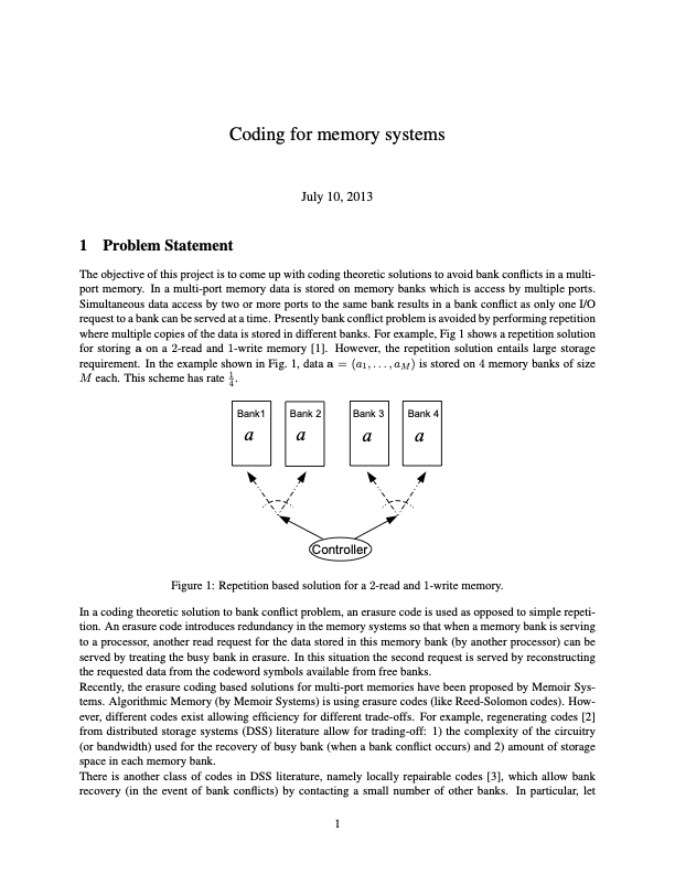
Problem Statement: Multi-port memories are essential for high-performance systems but suffer from significant complexity and space requirements in existing designs. This paper seeks to address these issues by proposing an innovative solution that leverages coding techniques.
Solution (Core Technology): The authors introduce a framework where data is encoded across multiple single-port memory banks, effectively emulating multi-port memory functionality through algorithmic means. By distributing the load of read requests across different memory banks, they reduce latency and storage overhead compared to traditional replication methods.
Key Achievements: Three coding schemes are proposed with significantly reduced storage overheads. The system demonstrates improved performance in critical word read and write latencies when compared to conventional uncoded designs. Performance gains were most notable under high-density access traces.
Significance & Applications: This work provides a novel approach to achieving multi-port memory functionality without the drawbacks of traditional designs, potentially enabling more efficient and less complex memory systems for various high-performance computing applications.
📄 Full Paper Content (ArXiv Source)
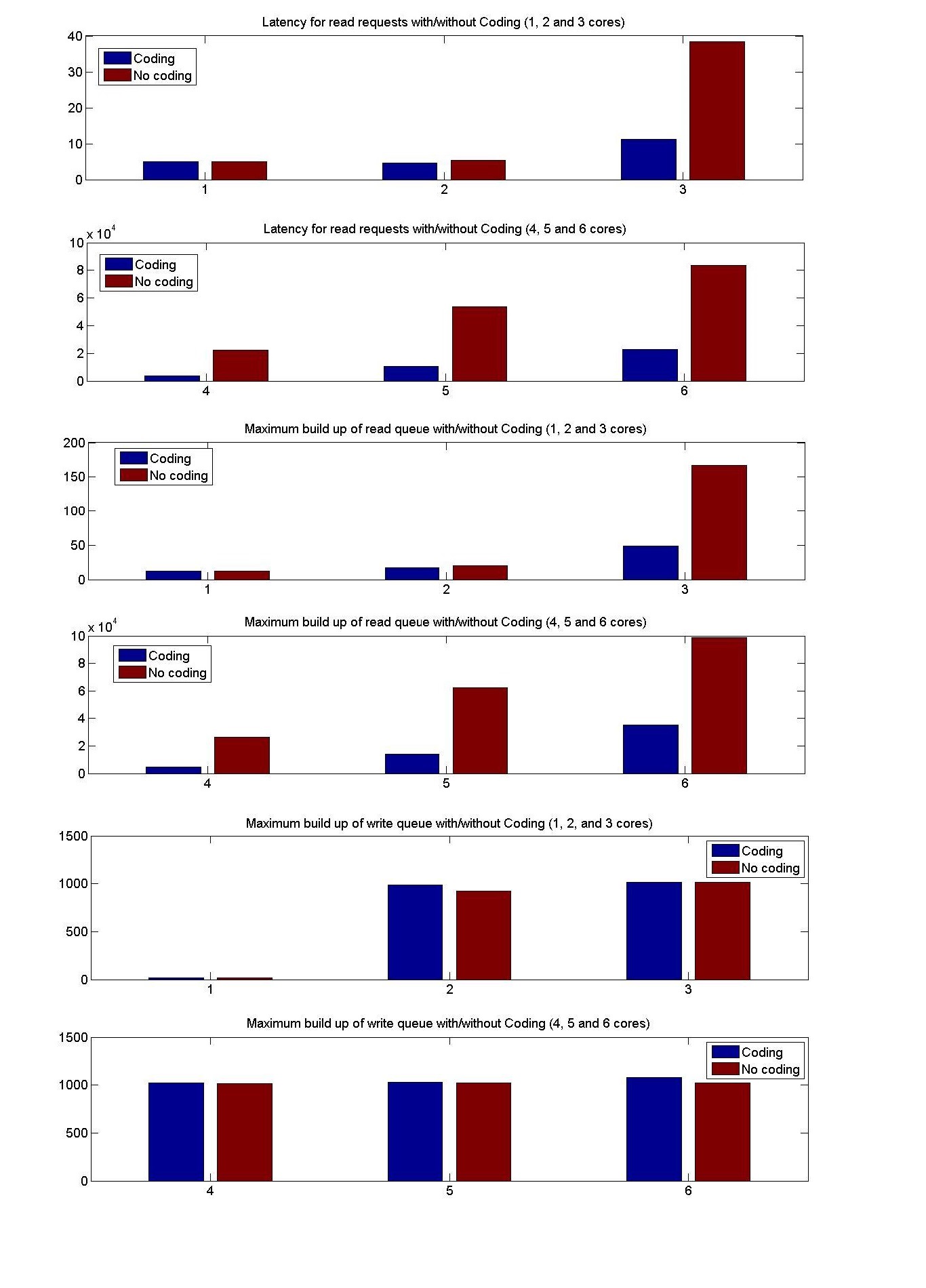
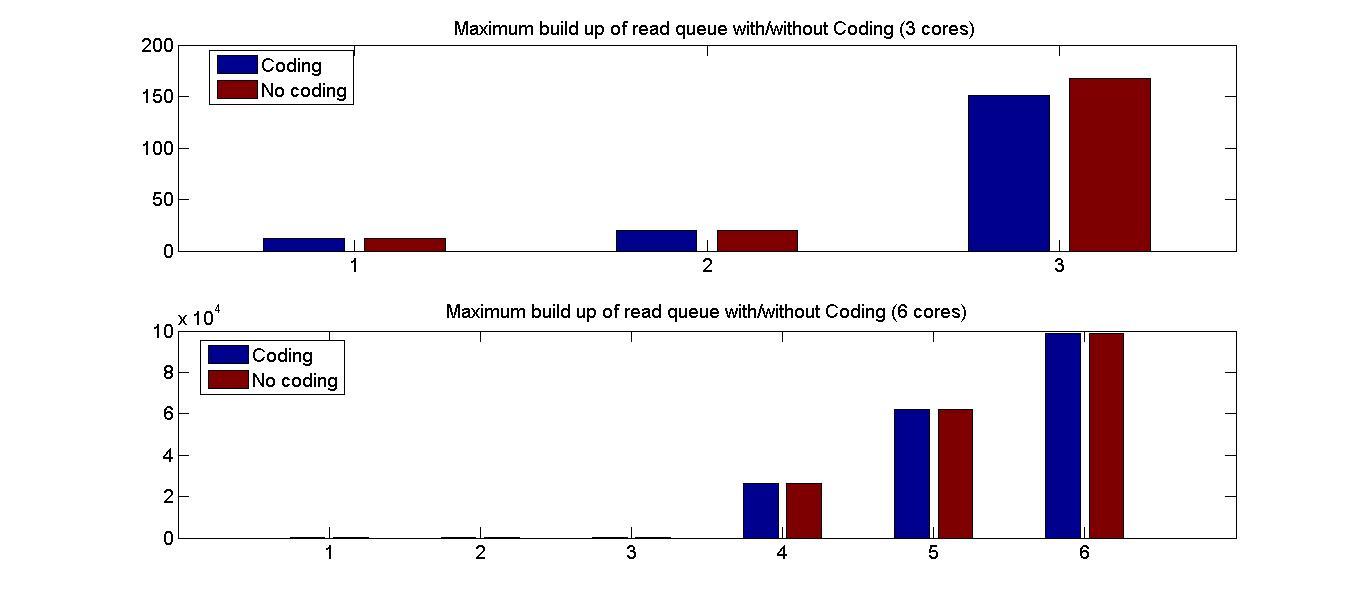
# SystemC implementation Results
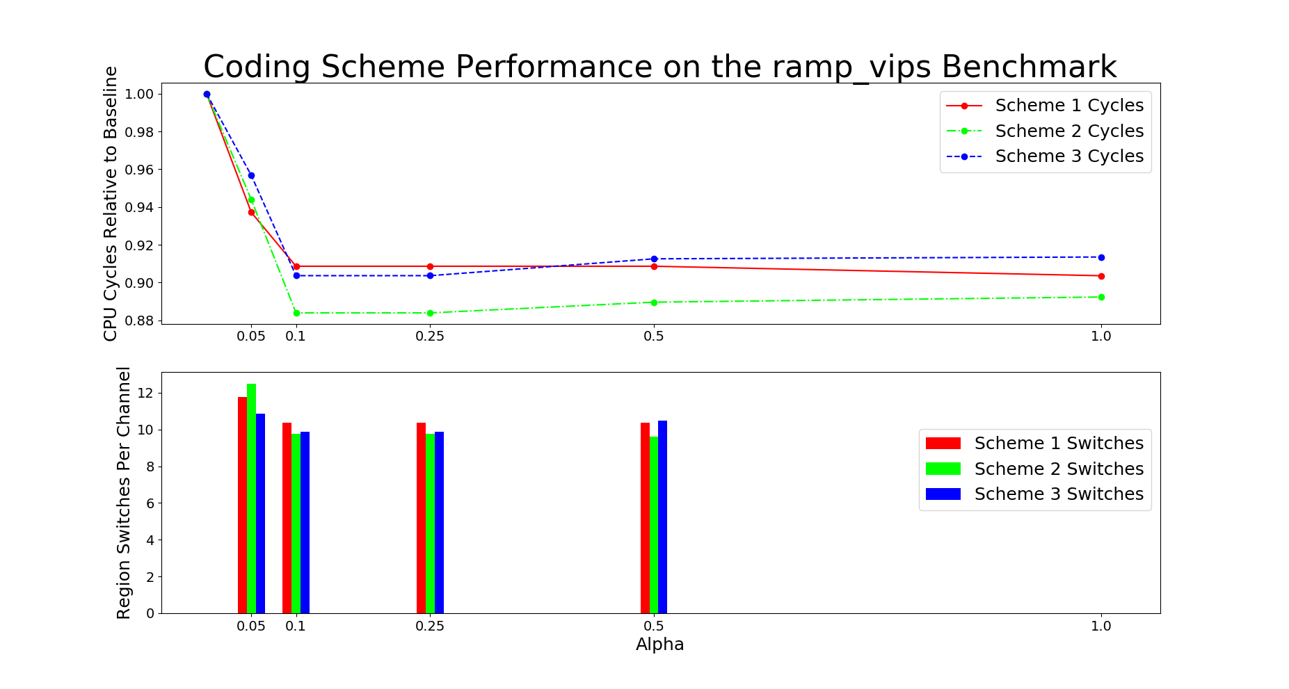
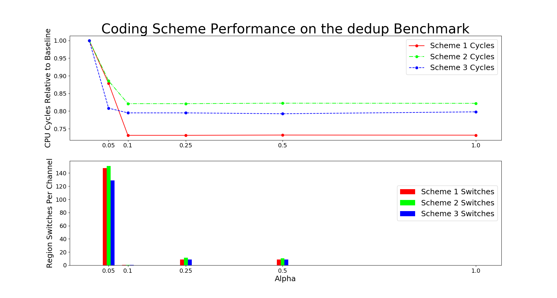
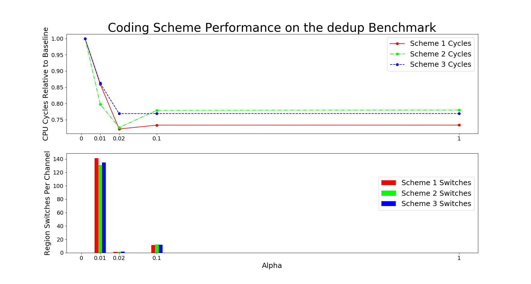
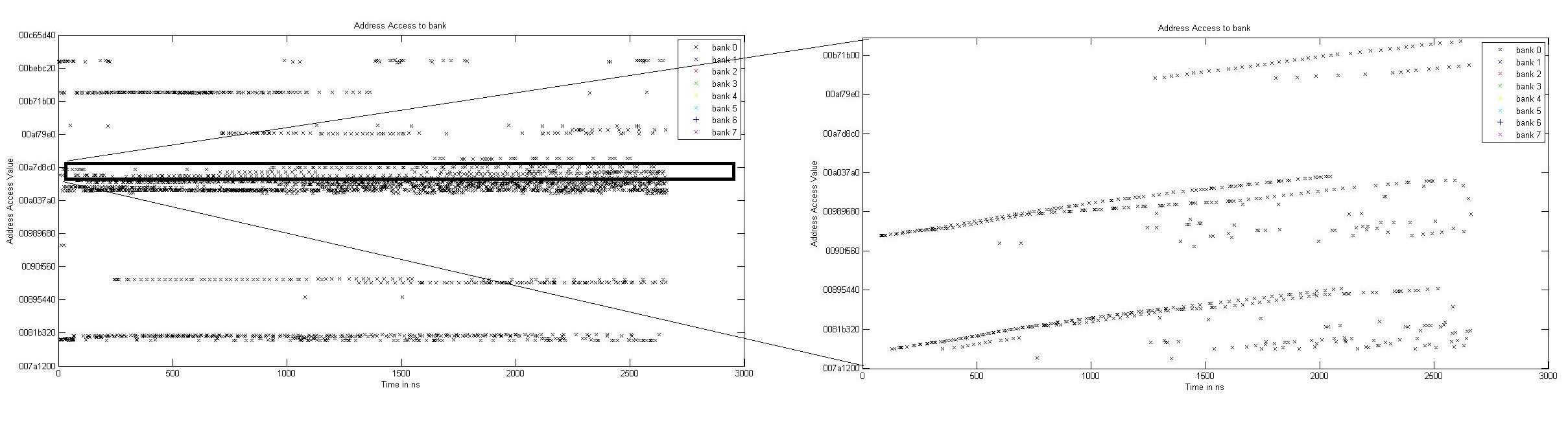
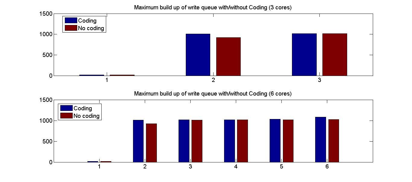
This section describes the performance results for simulation of code
designs on systemC platform. We implement system C model of the memory
controller with code design 1 as described in figure 3. The model is
used as a simulator with input as memory access traces. The simulator
logs the latency of each memory request.
The traces are essentially a list of access requests with a field for
time. These request act as command to the memory controller.
The performance charts for each traces comprise of four metrics as
described below.
Critical Read Latency This parameter is the average latency
experienced by the most critical word of a read request. This metric
is averaged over the whole execution of the trace. Evident from its
name, critical word releases the processor from the stall and the
other memory elements in the cache line can follow it. The critical
read latency is calculated by taking an average of critical read
latency of all the requests from all 6 cores.
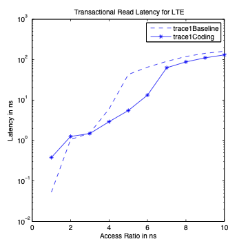
Transactional Read Latency is the latency of the whole read memory
request. This is also averaged over the whole execution of the trace,
i.e., over requests from all the cores. This determines the average
latency of read accesses.
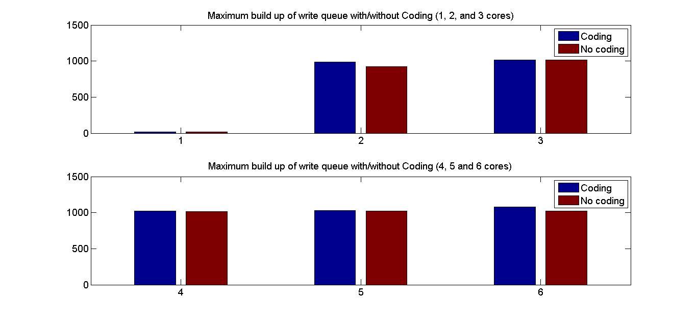
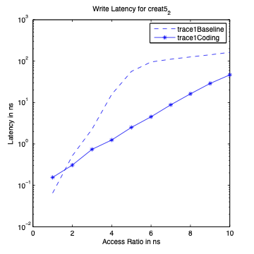
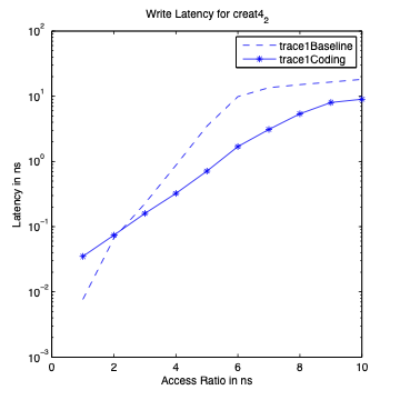
Write Latency is the measure of average latency of write requests
before it is committed to the memory. This does not account for the
latency caused by reCoding. Since the cost of recoding is embedded in
the cost of future read/writes. The average is taken over all the
requests received by the memory controller over all the cores.
Trace Execution time is the time taken to process a trace. This is
a direct representation of overall system efficiency.
Some Important Notes:
The access ratio in the x-axis means
$`\frac{\text{speed of cores}}{\text{speed of memory}}`$
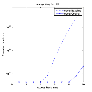
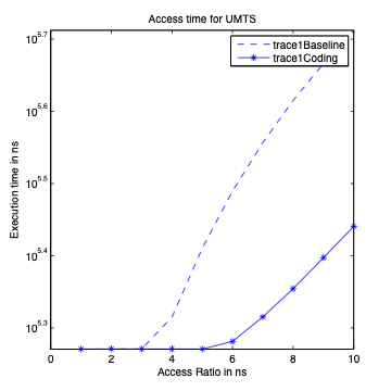
The y-axis on the Trace Execution Graph is in linear scale with time
in ns.
In the simulation for Design II, we implement the inter bank coding,
however, we have not yet explored the benefit of intra-bank coding
introduced in Design II.
The cost of Design II reduces from $`2.5 \alpha`$, since we don’t
consider the cost of storing intra bank codes.
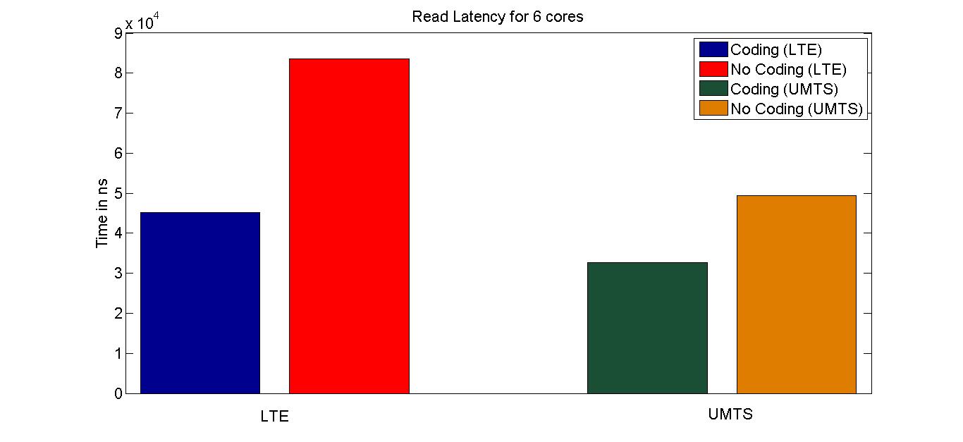
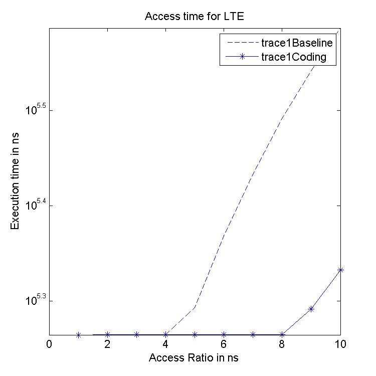
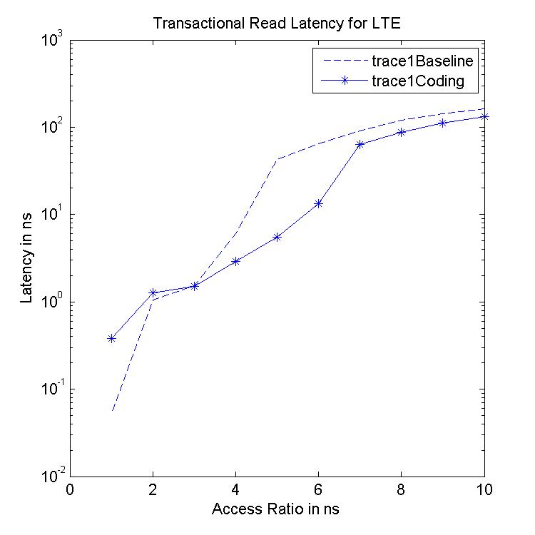
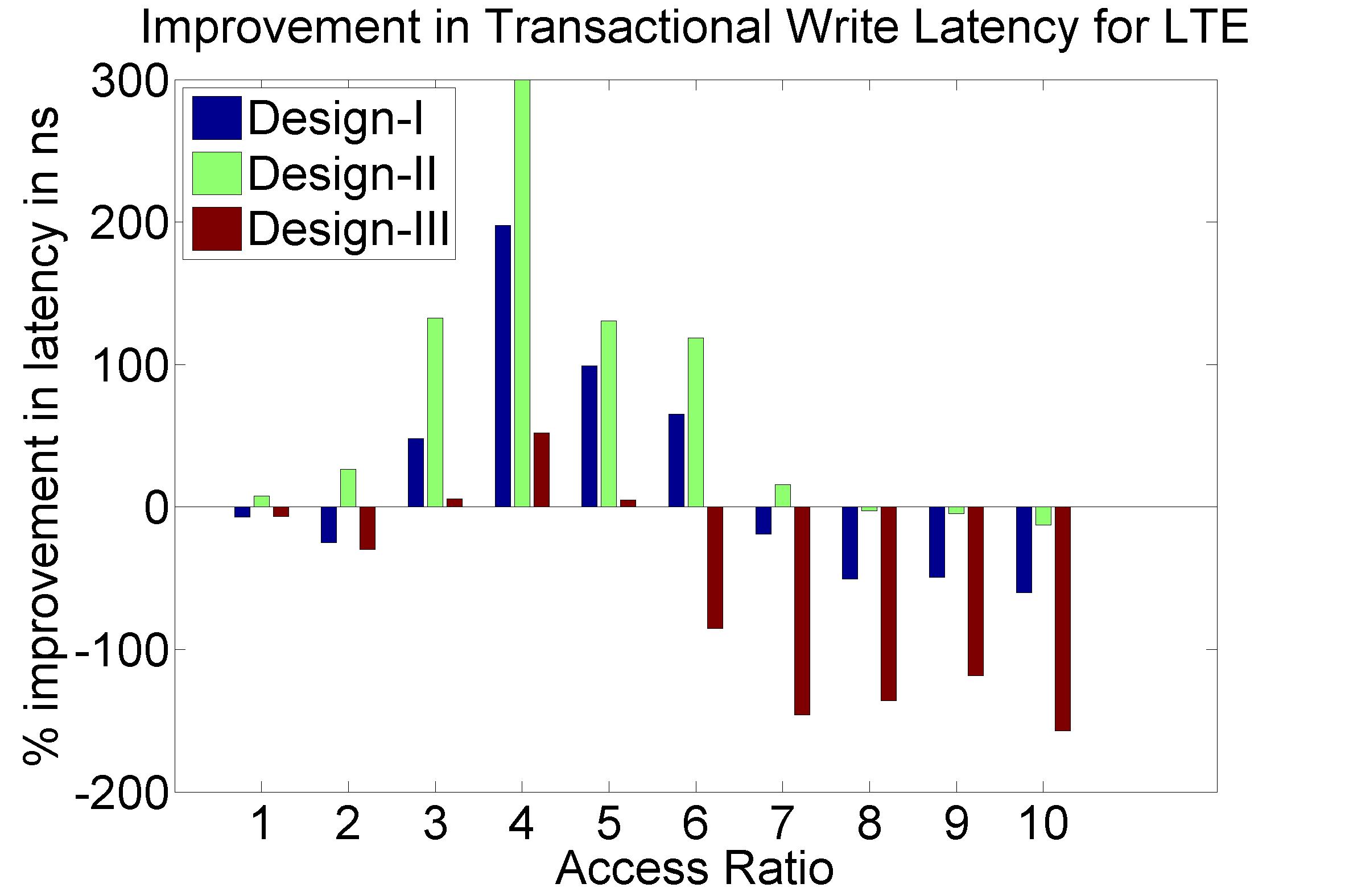
Performance Graphs for LTE
trace
Performance Graphs for LTE
trace
Observations:
LTE trace is a medium density trace.
The benefit for coding for read access is favourable for access ratios
for 4 and more.
The write transaction latency shows improvement for access ratios of 3
to 6.
The coding benefits are best at access ratio of 4, 5 and 6.
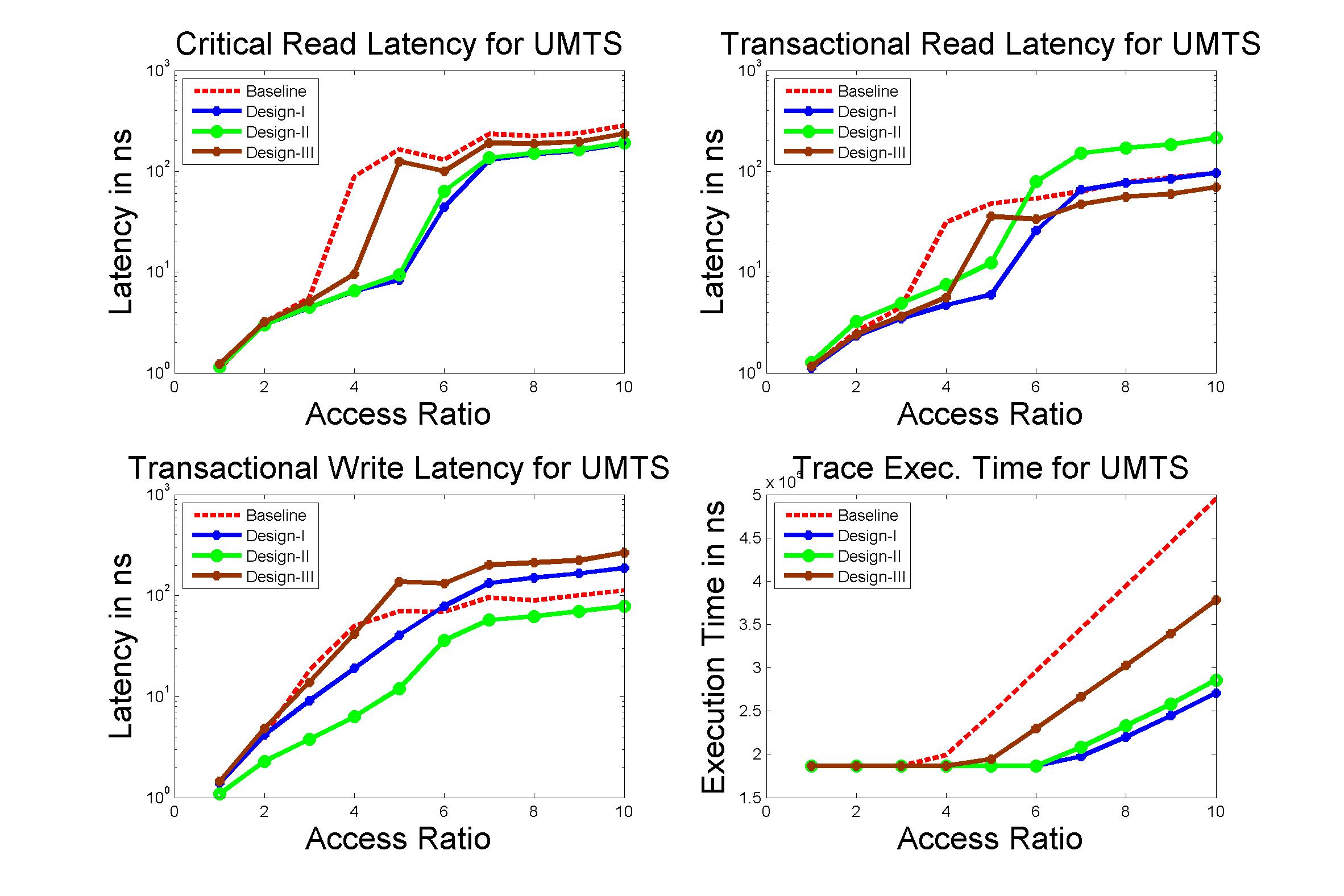
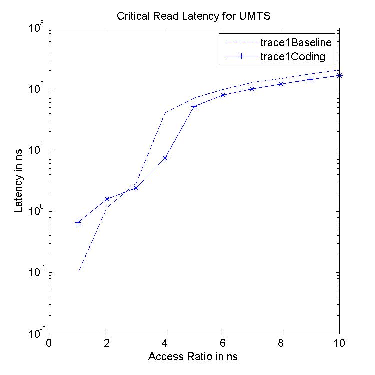
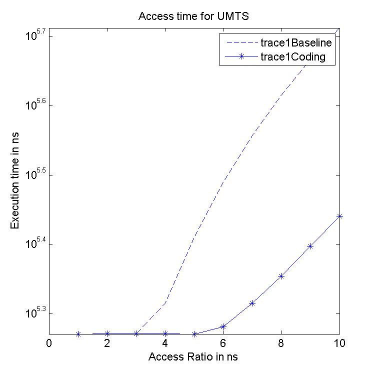
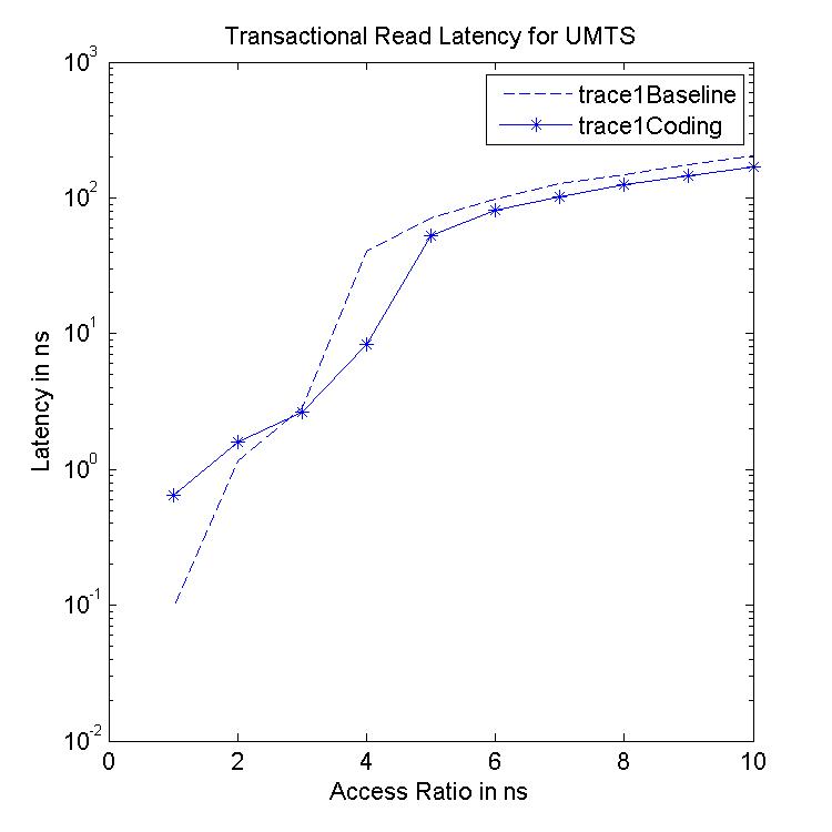
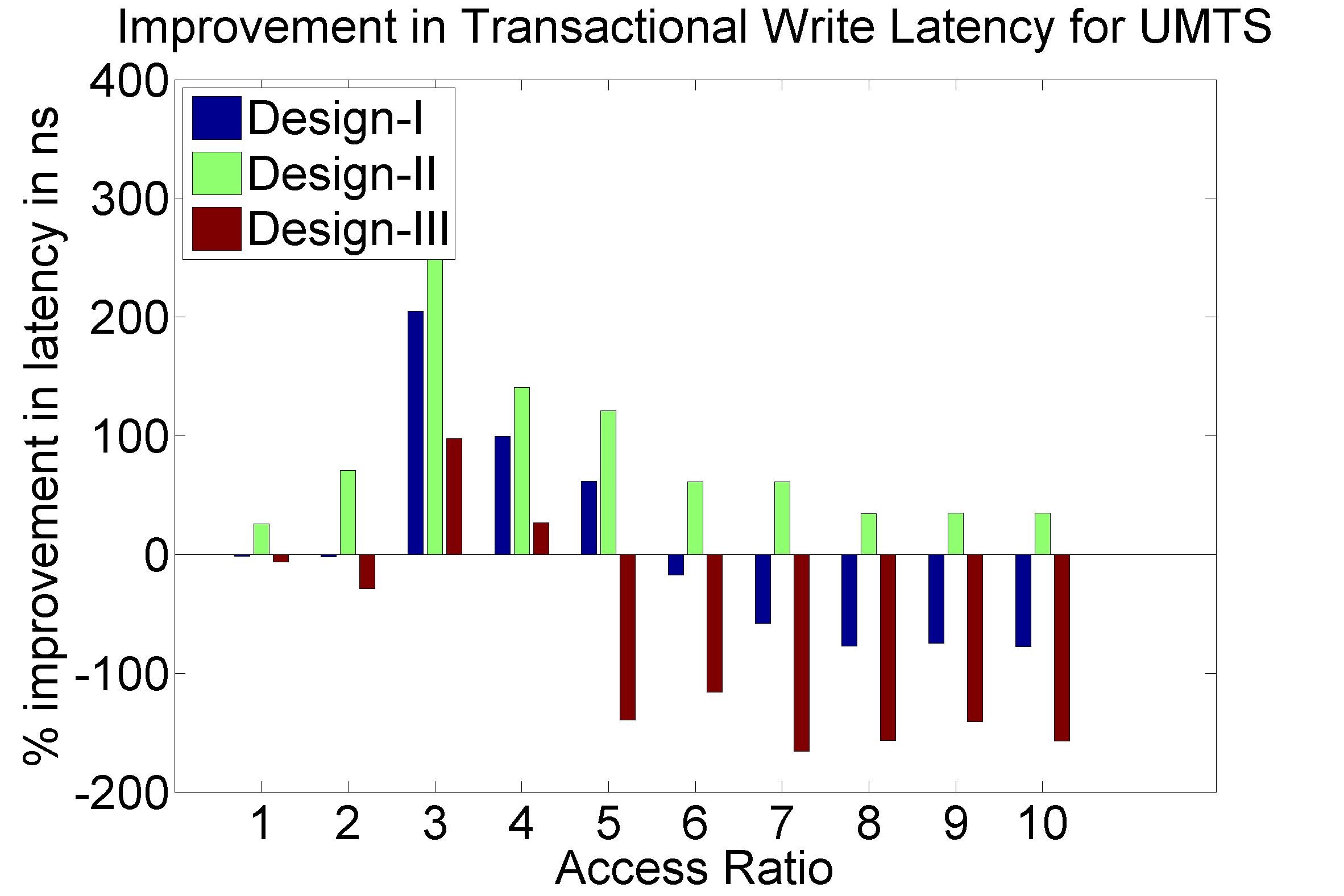
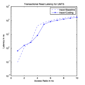
Performance Graphs for UMTS
trace
Performance Graphs for UMTS
trace
Observations:
The UMTS trace is also a medium access trace.
The read latency improvement in UMTS is substantial for all access
ratios in case of critical latency.
The Transactional Latency improvees untill access ratio of 6.
The design II sees degradation in performance for higher access
ratios.
Write Latency improvement is observed for access ratio of 3 and 4.
The coding benefits are best at access ratio of 4.
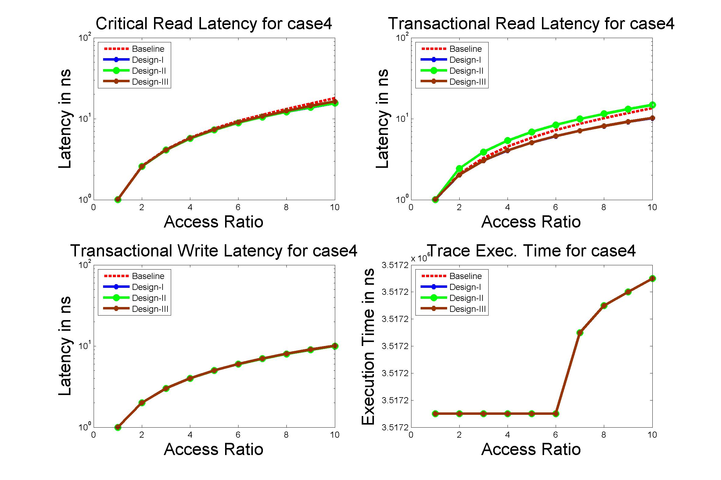
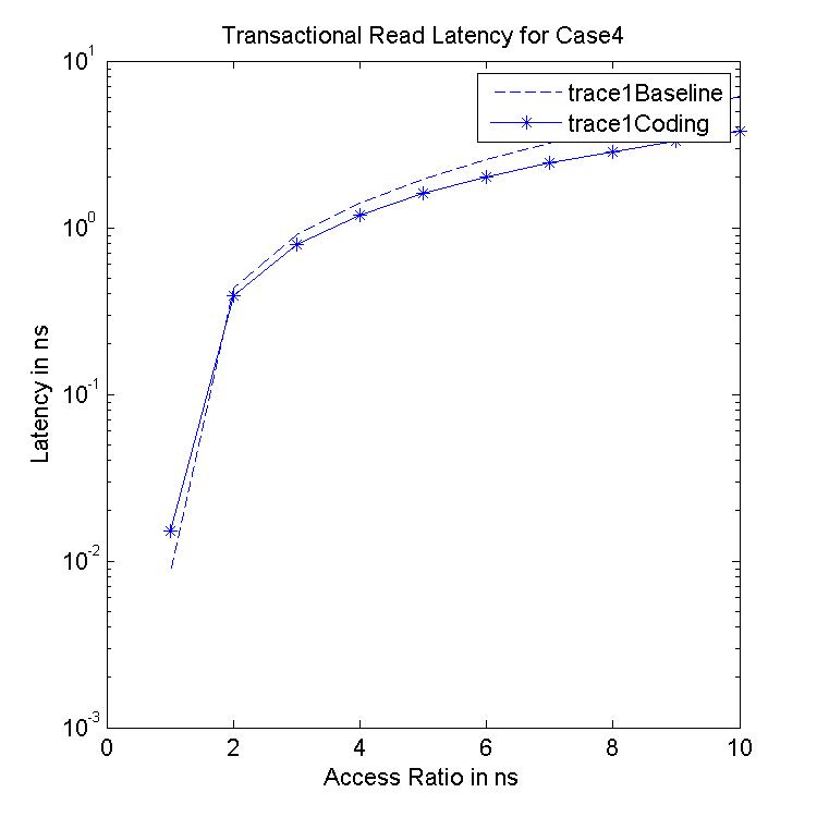
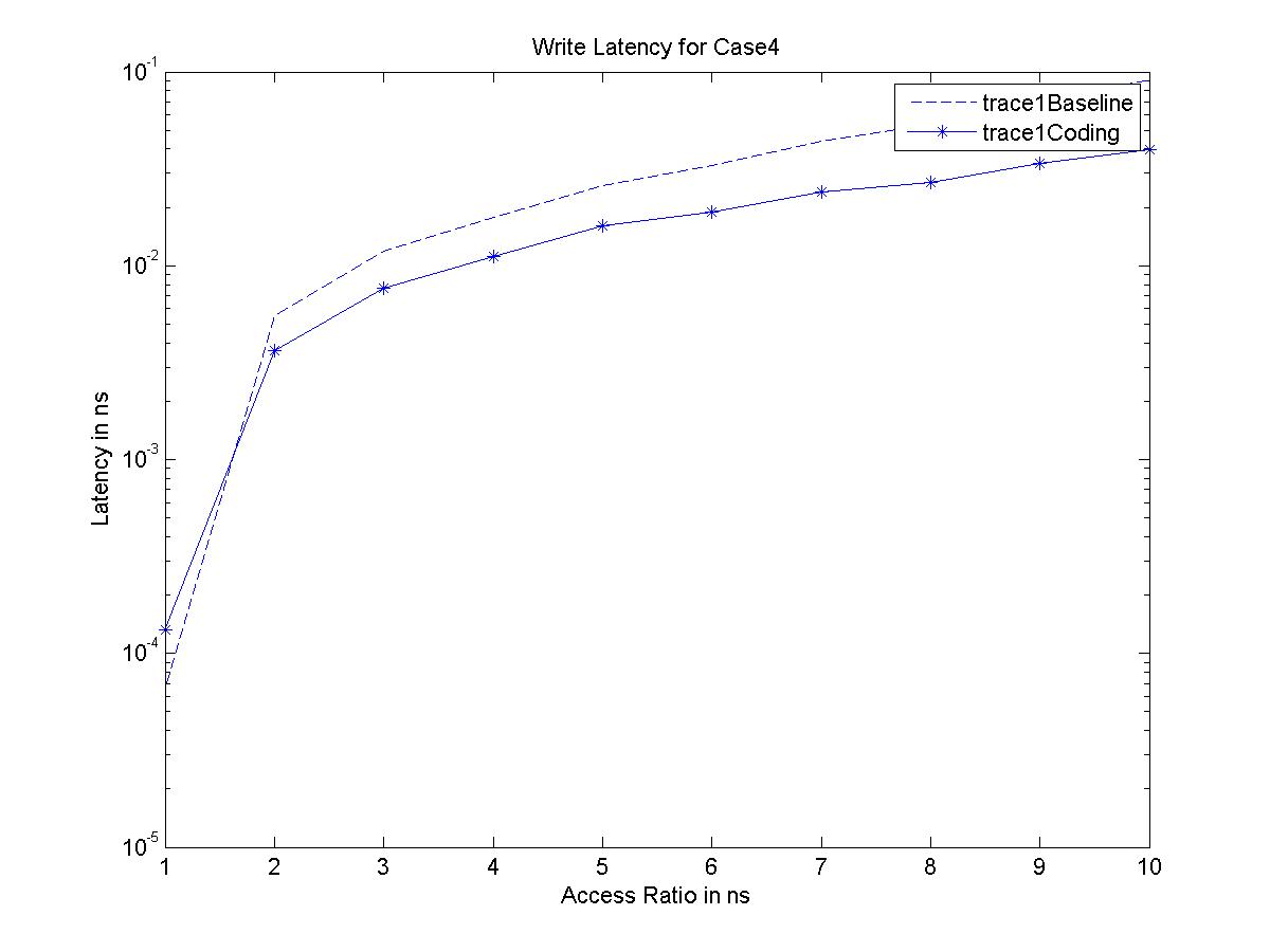
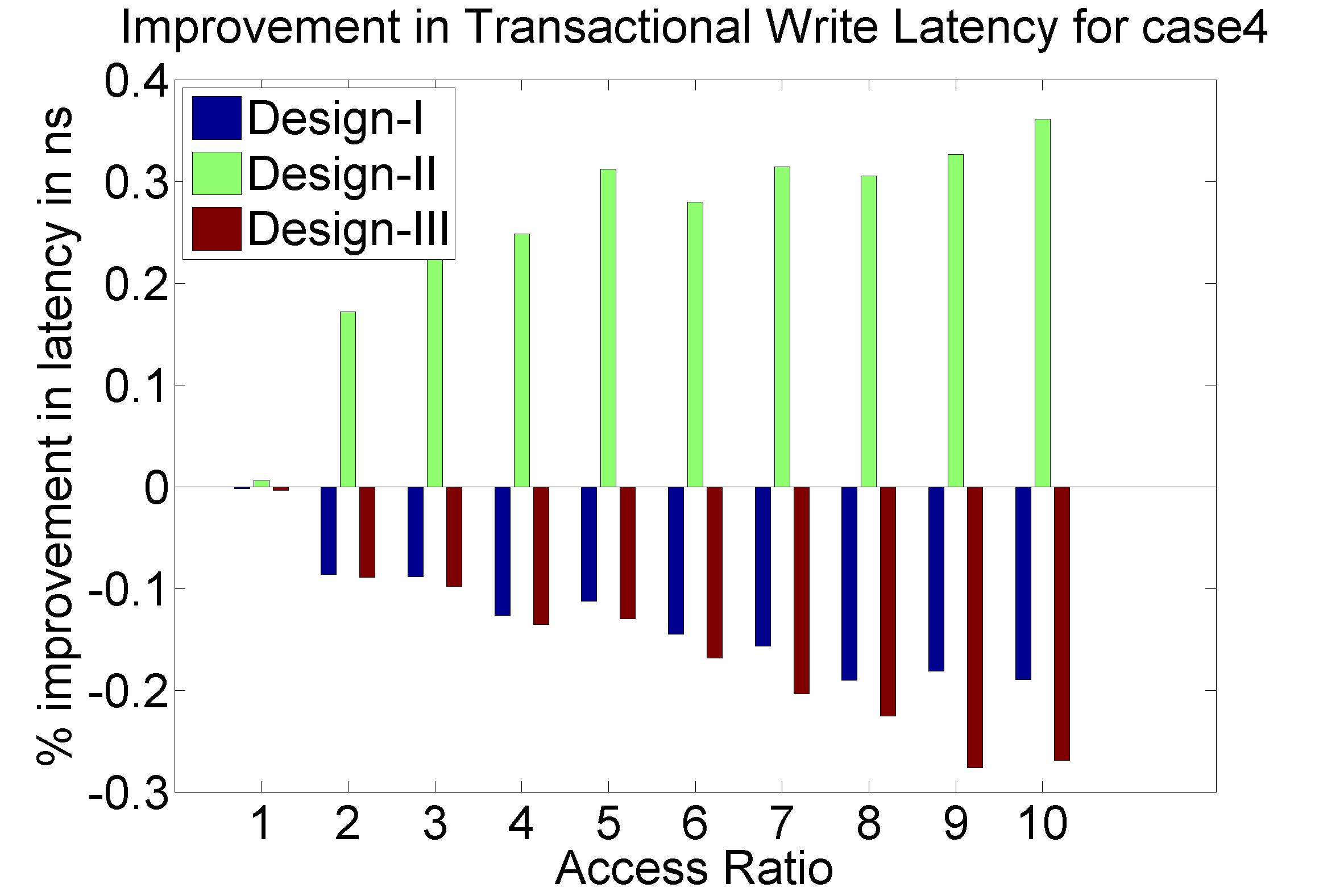
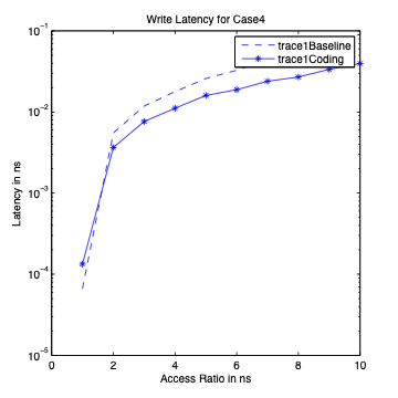
Performance Graphs for case4
trace
Performance Graphs for case4
trace
Observations:
The case4 traces are low density traces. That is, the number of access
requests per time period are low.
The Critical Read latency improvement in positive for all the
ratios.
The critical read latency exponentially improves for increased access
ratios.
The transactional Read latency also improves for design I and design
III.
The write latency has only marginal improvement.
The results suggest that in case4, we do not use the “coding” aspect
due to low density access in case of Writes.
The improvement in Transactional Read Latency is substantial.
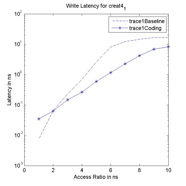
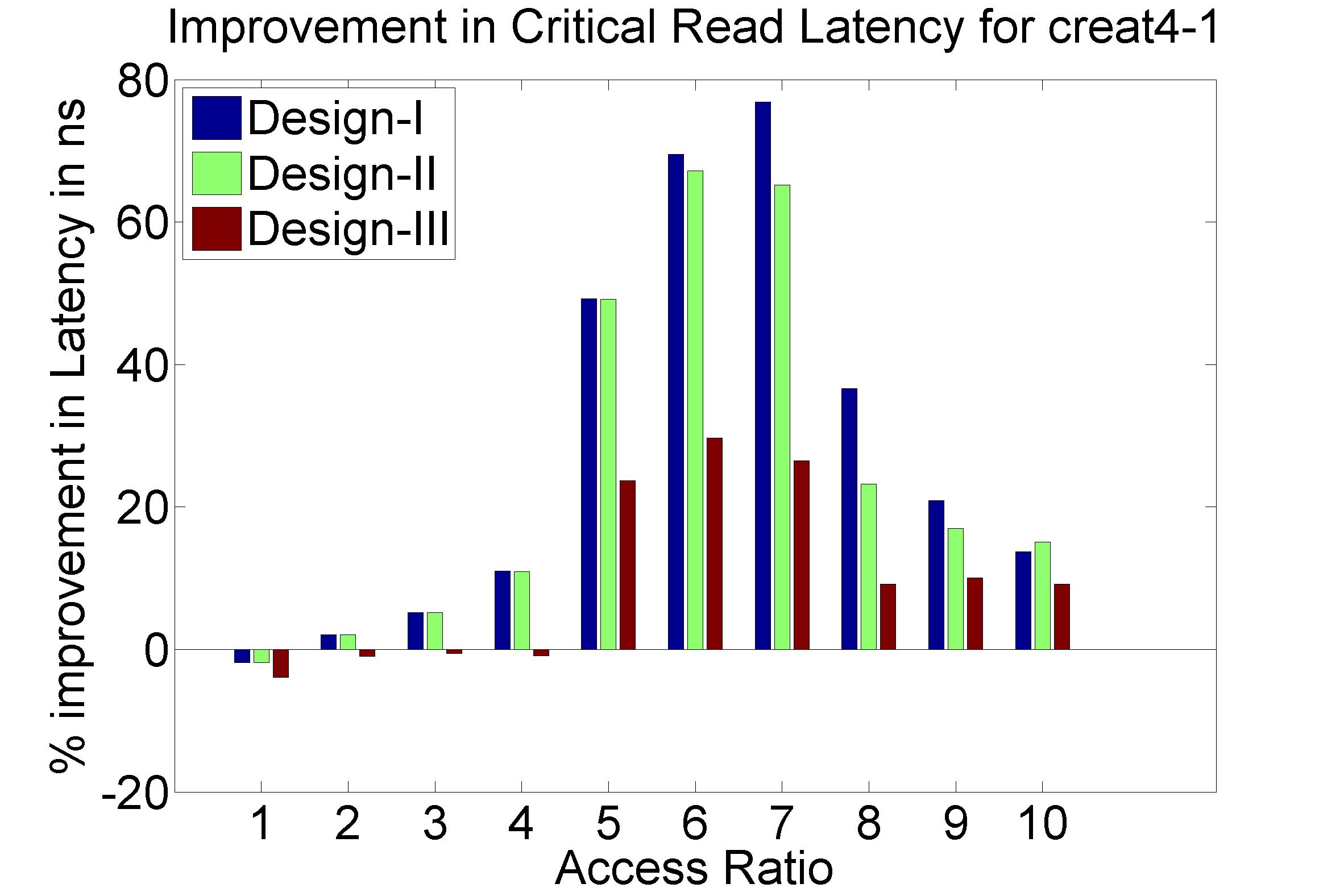
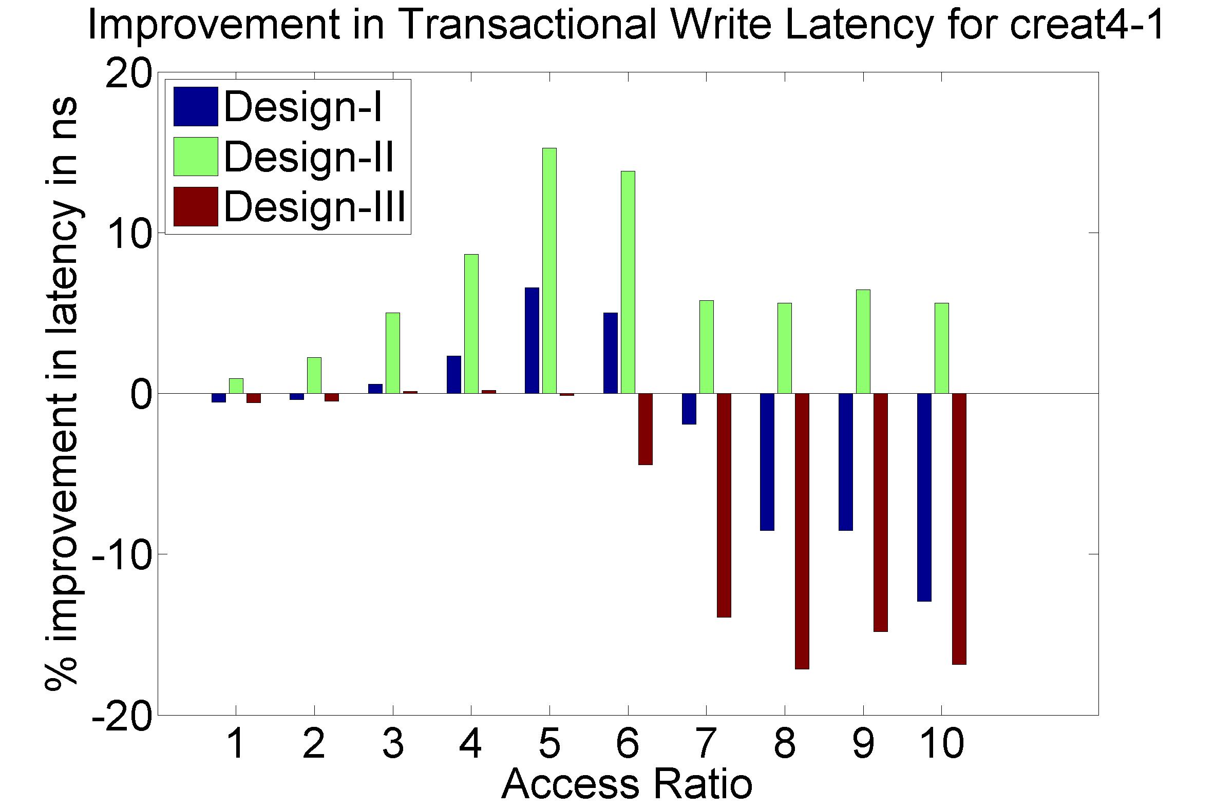
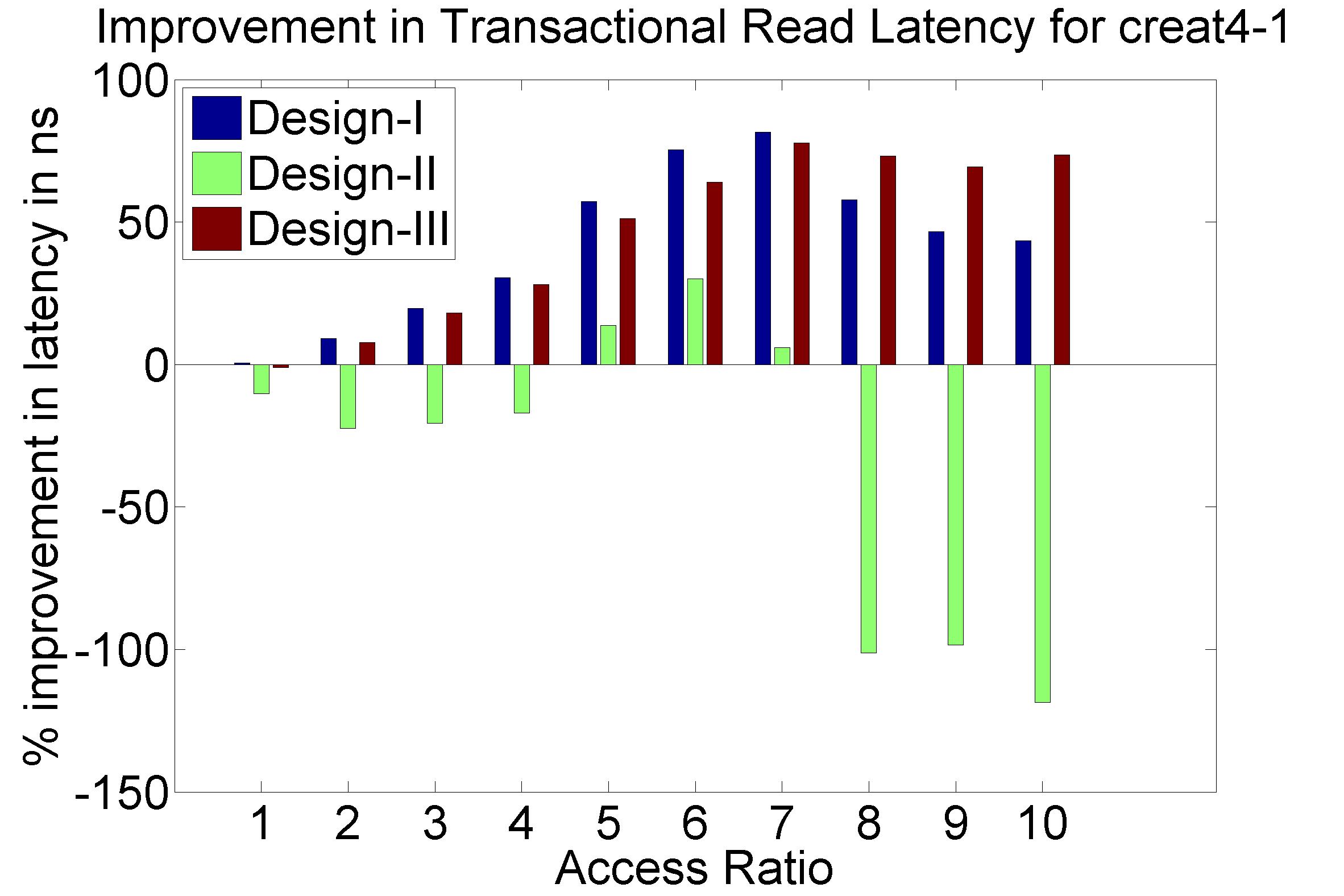
Performance Graphs for Creat4-1
trace
Performance Graphs for Creat4-1
trace
Observations:
The trace creat4-1 is a medium density trace.
The improvement in critical read latency and transactional read
latency is significant in design I and design II.
The write latency is positive till access ratio of 6.
Design I and Design III codes benefit in this trace.
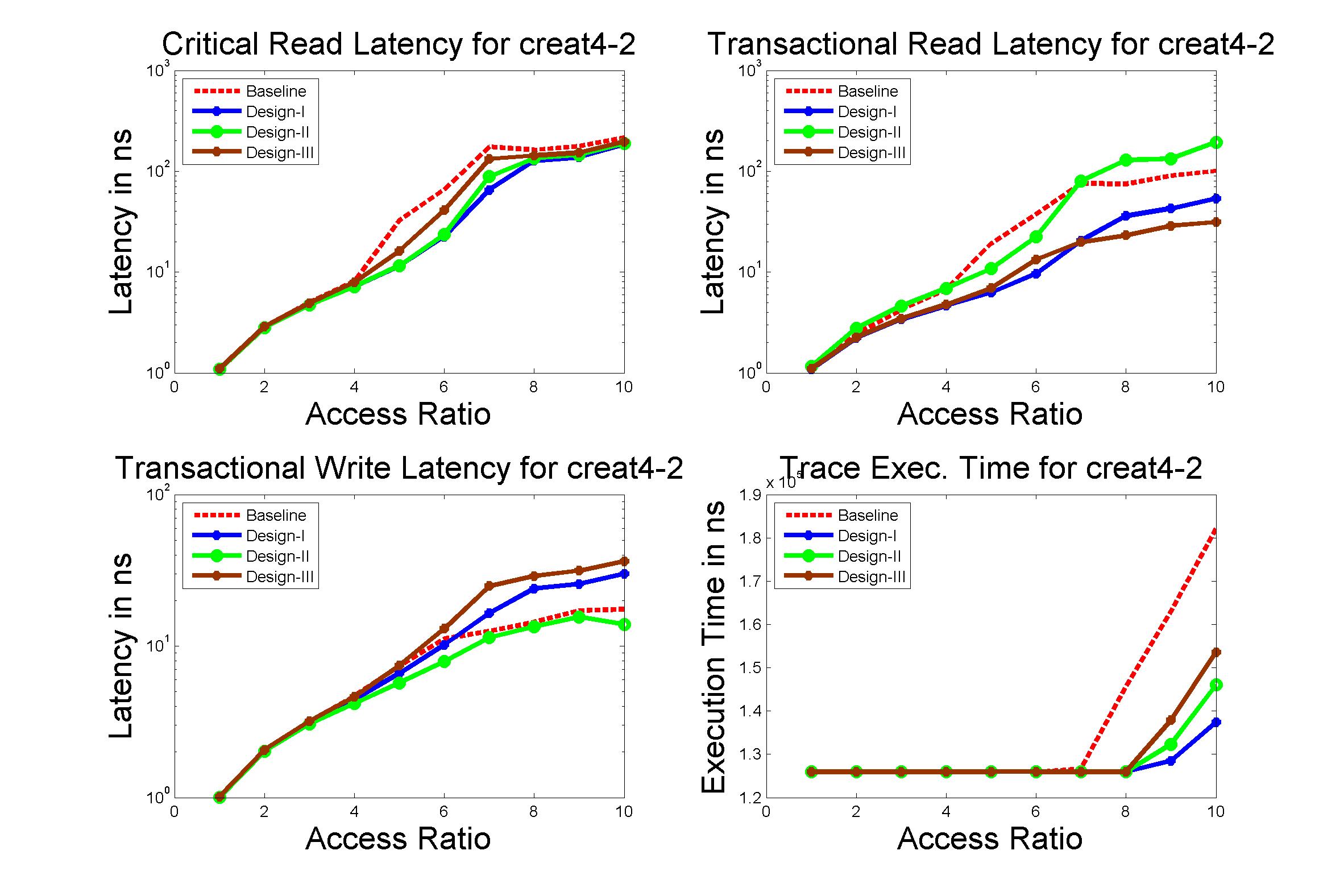
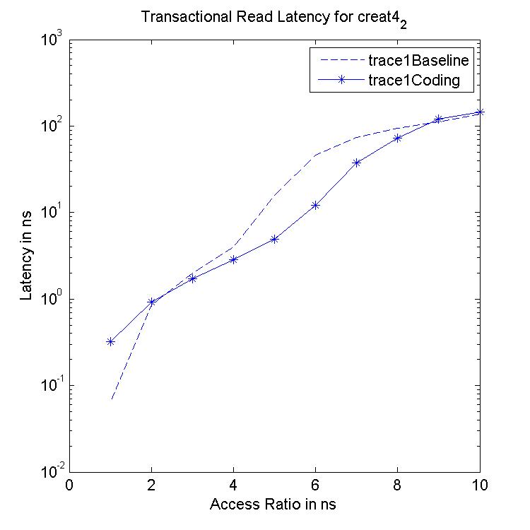
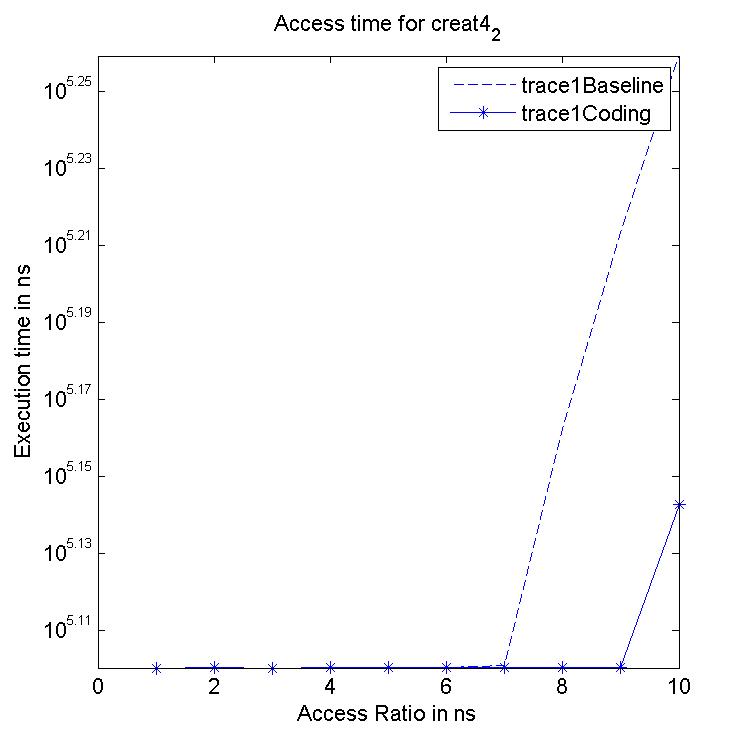
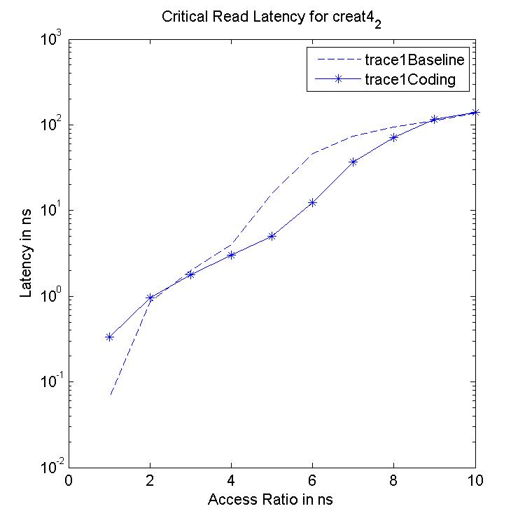
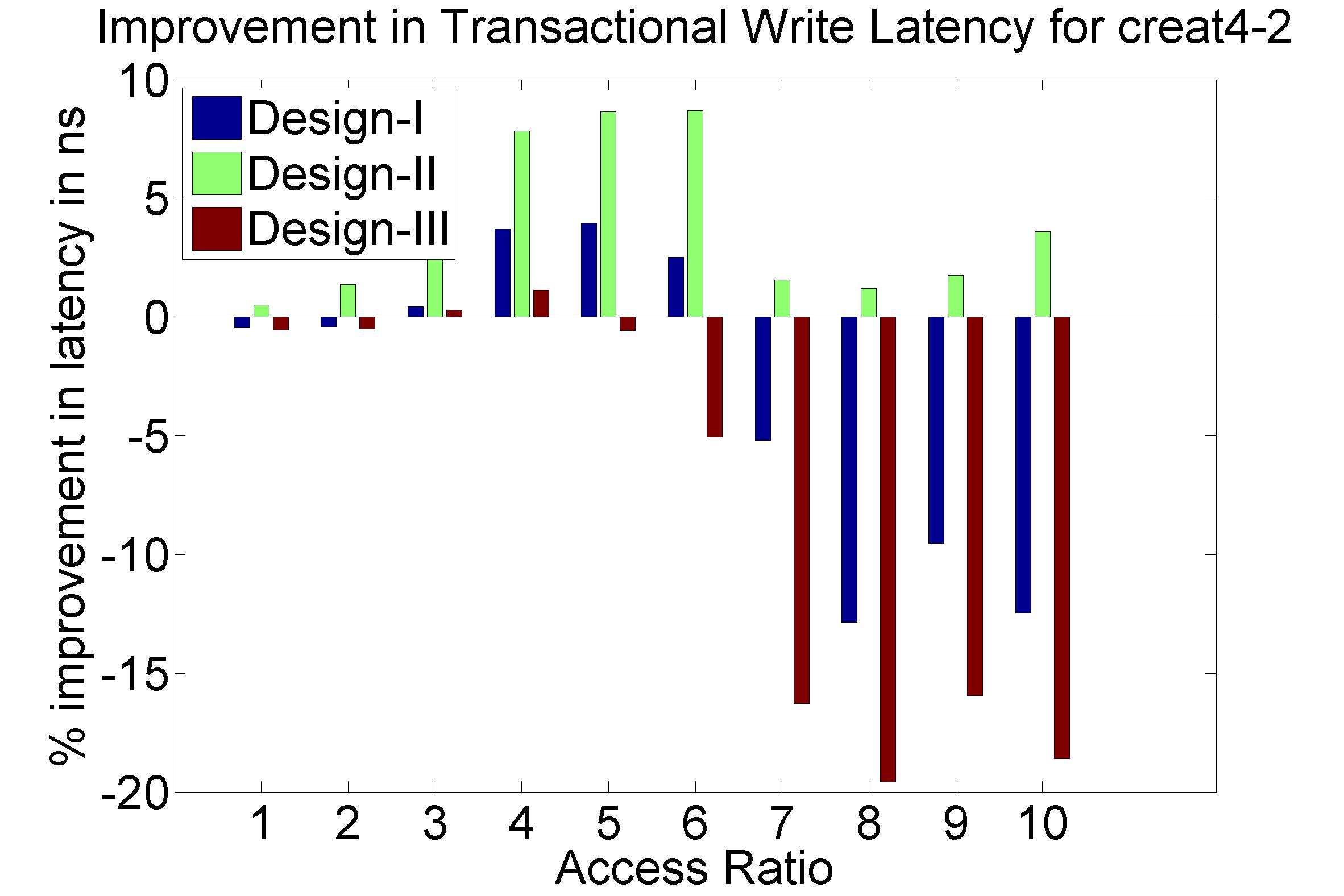
Performance Graphs for Creat4-2
trace
Performance Graphs for Creat4-2
trace
Observations:
This trace is second part of Creat4 trace.creat4-2 is a medium density
trace.
The improvement in critical read latency and transactional read
latency is significant in design I and design III.
The write latency is positive till access ratio of 5.
Design I and Design III codes benefit in this trace.
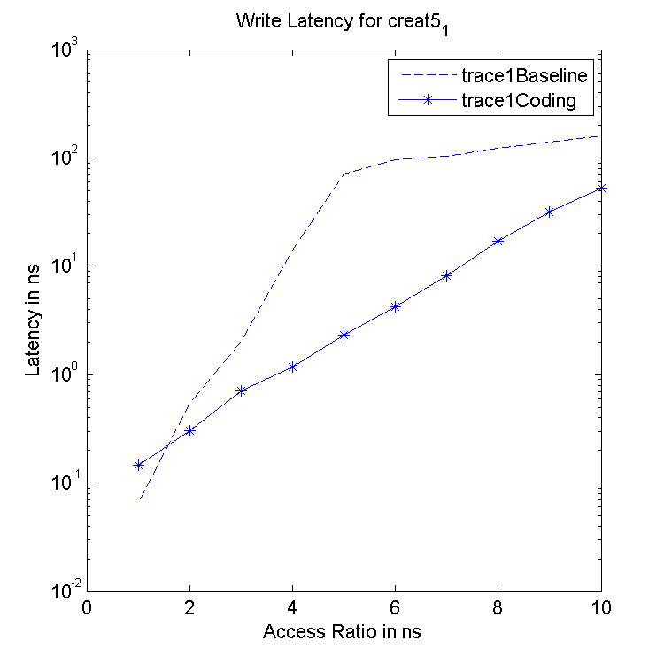
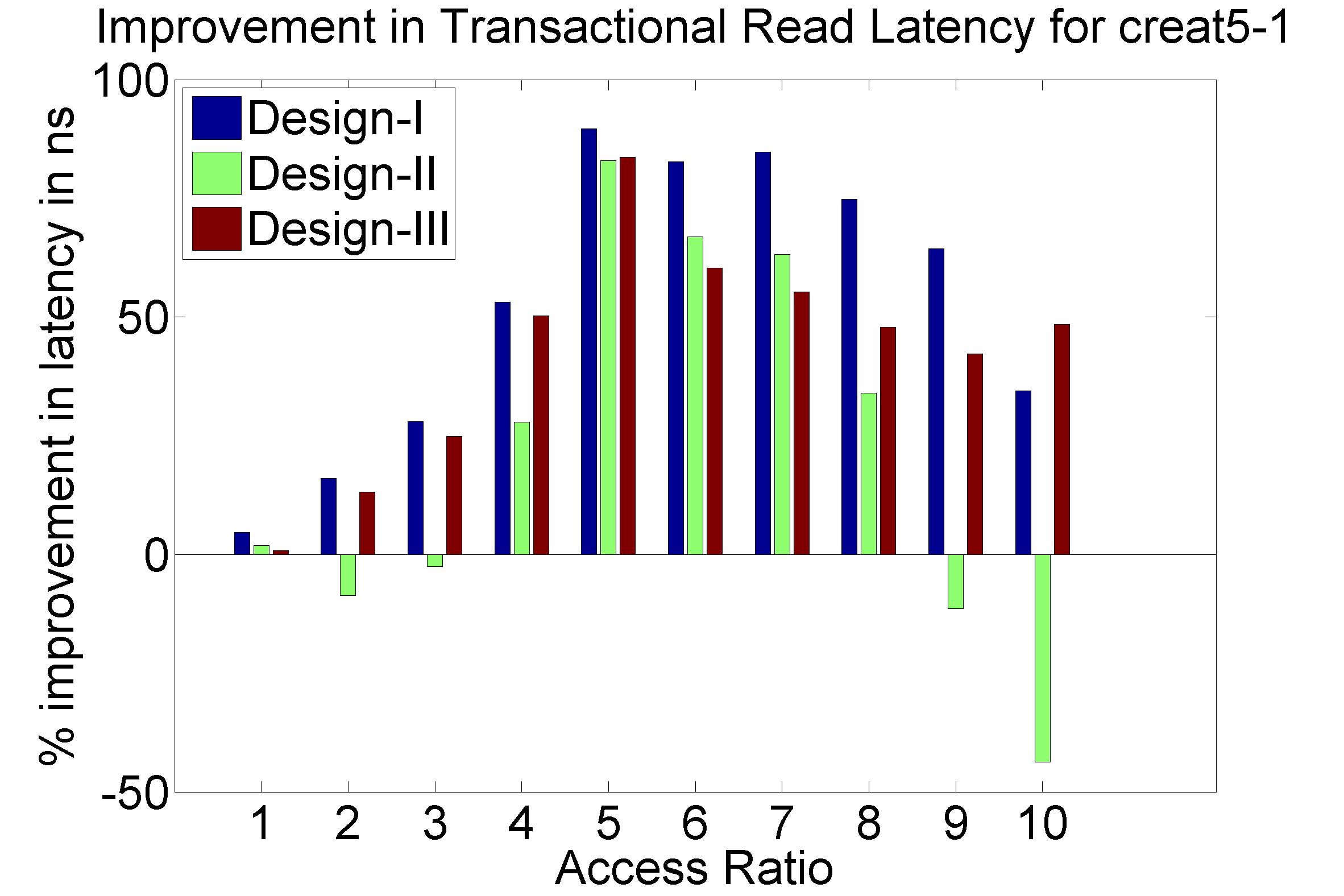
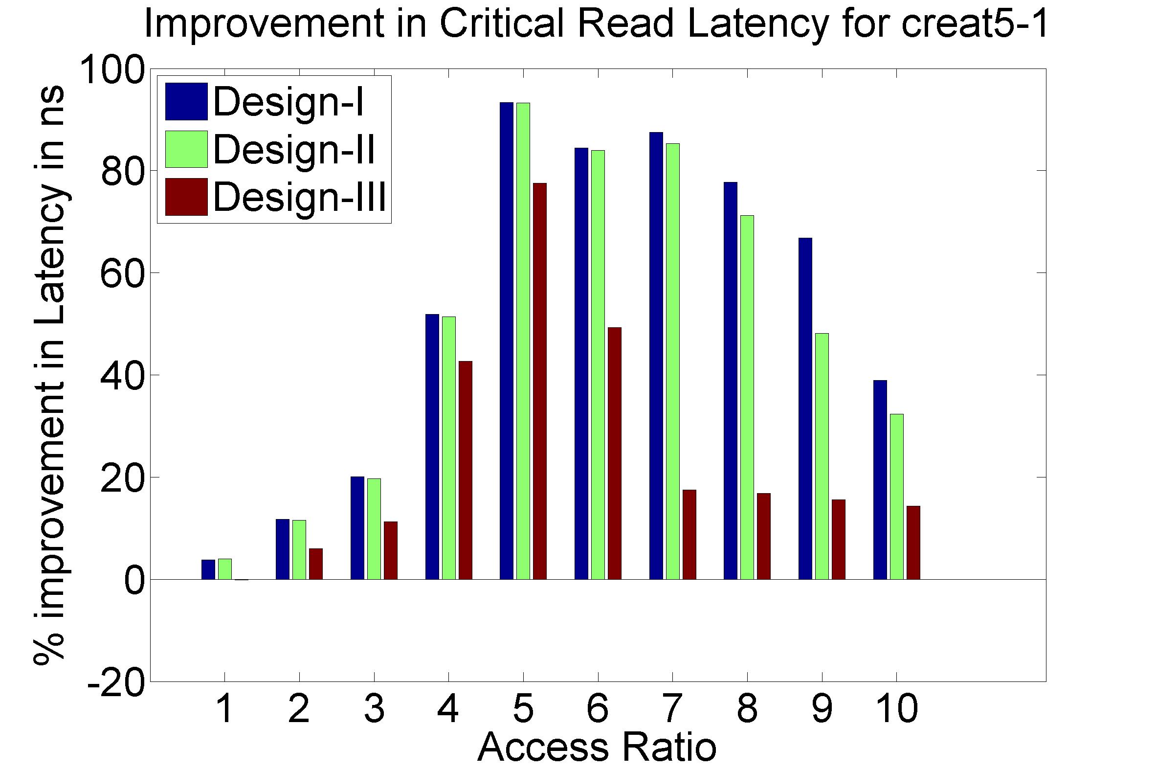
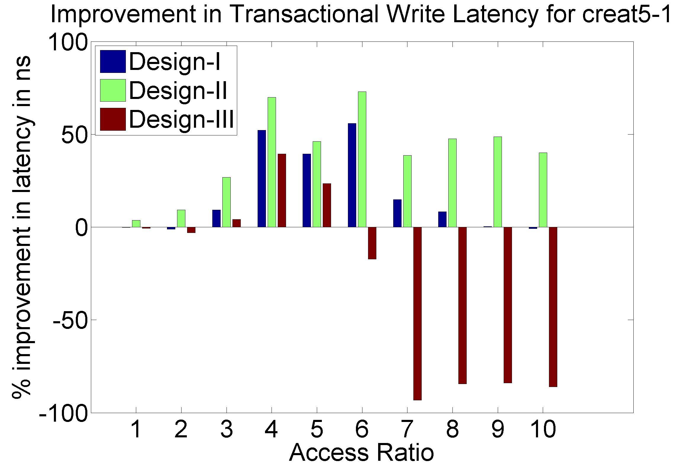
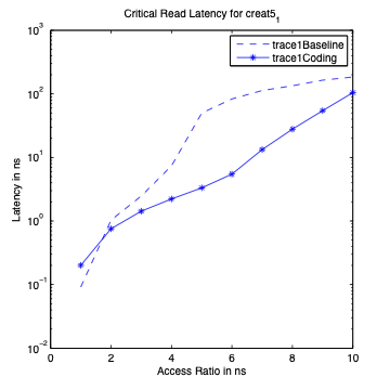
Performance Graphs for Creat5-1
trace
Performance Graphs for Creat5-1
trace
Observations :
Creat5-1 is a high density trace.
There is a significant critical read latency improvement for all
access ratios in all design.
The transactional read latency is improves for all access ratios.
The write access latency improves for access ratio between 3 and 6.
All the code designs are ideal for this trace.
Coding architecture is ideal for this trace.
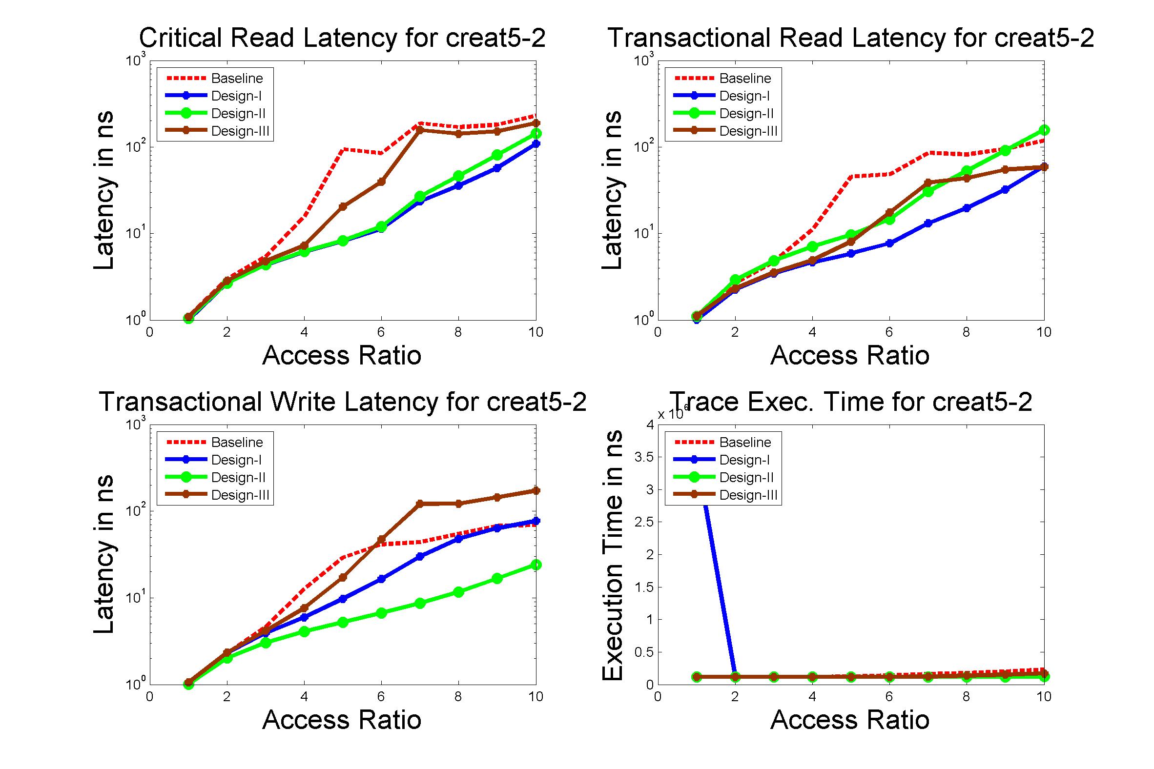
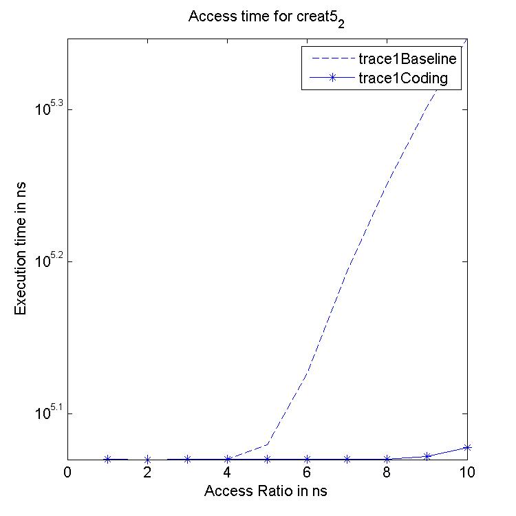
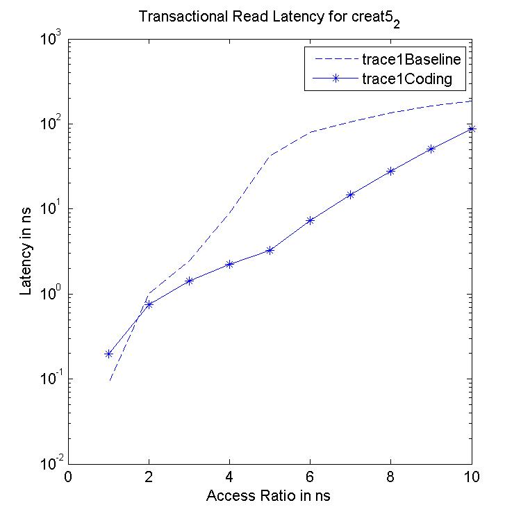
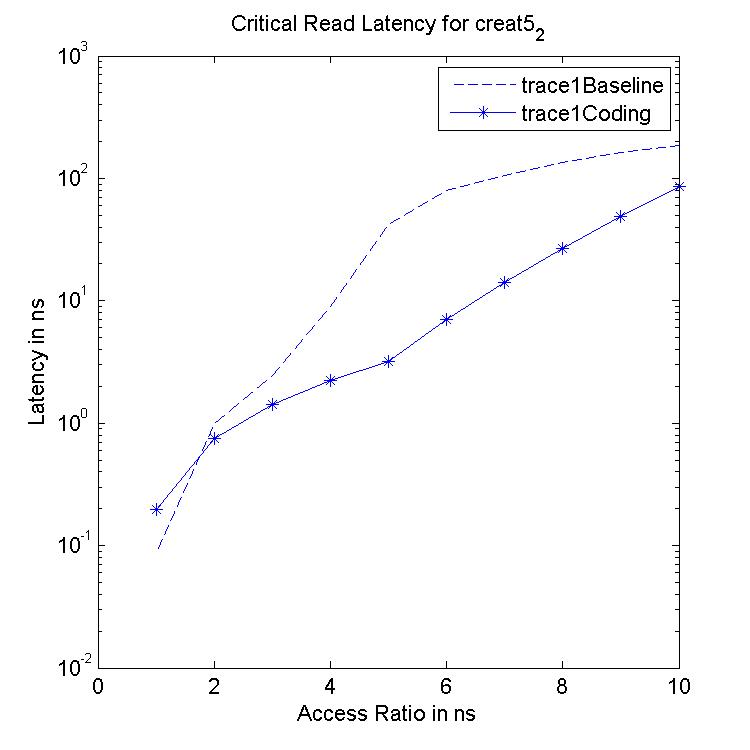
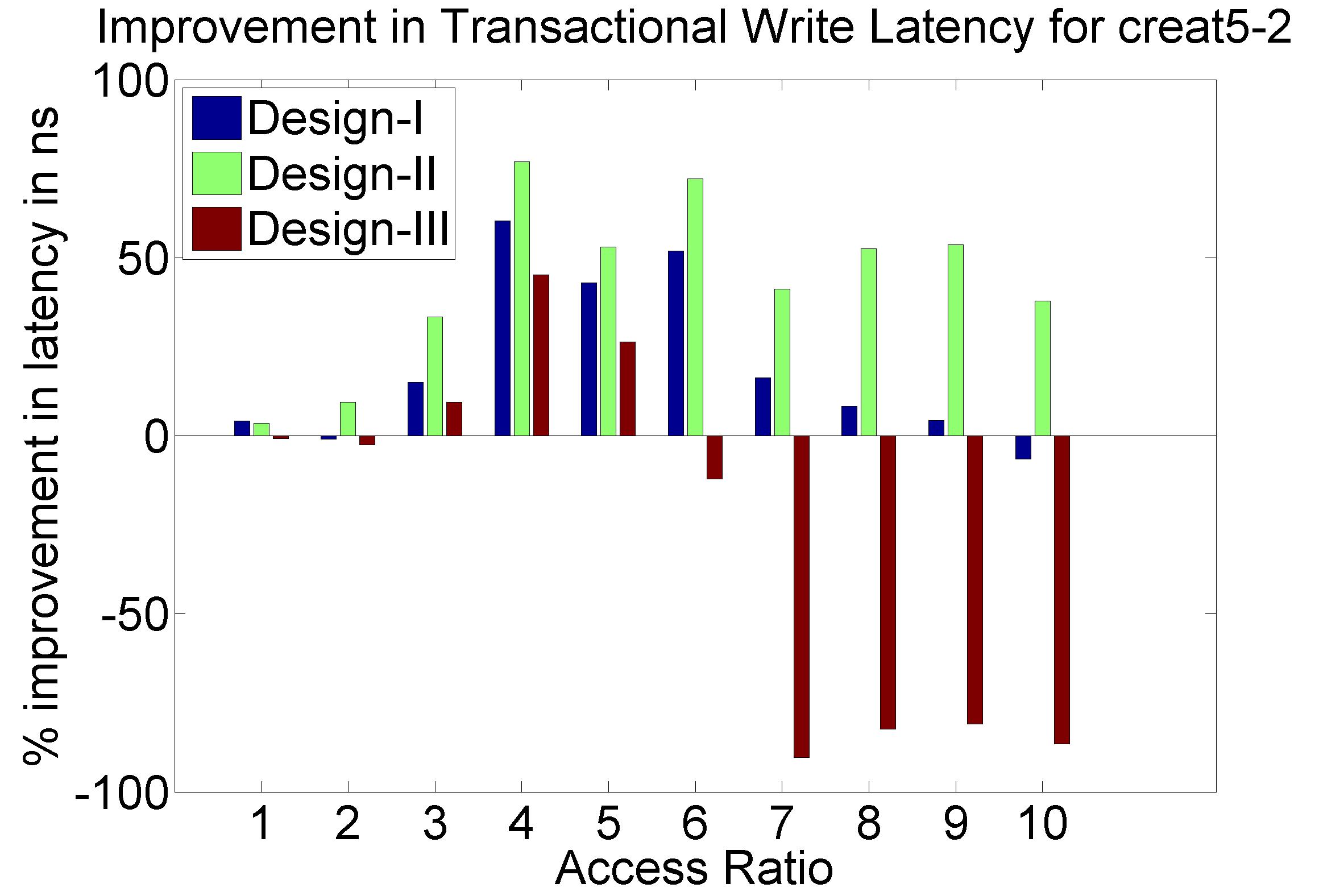
Performance Graphs for Creat5-2
trace
Performance Graphs for Creat5-2
trace
Observations :
Creat5-2 is a part of Creat5 trace. Creat5-2 is a high density trace.
There is a significant critical read latency improvement for all
access ratios in all design.
The transactional read latency improves for all access ratios.
The write access latency improves for ratios between 3 and 6.
Access Ratio is defined as
$`\frac{\text{speed of cores in ns}}{\text{speed of memory in ns}}`$
Trace
Density
Critical Read Latency Improvement
Transactional Read Latency Improvement
Transactional Write Latency Improvement
Access ratio with 15-20$`\%`$ improvement for Read
Access ratio with 15-20$`\%`$ improvement for Write
LTE
Medium
Varies from -10 to 80$`\%`$
Varies from -50 to 80$`\%`$
Varies from -150 to 300$`\%`$
access ratio 4 to 10
access ratio 3 to 6
UMTS
Medium
Varies from -5 to 90$`\%`$
Varies from 0 to 80$`\%`$
Varies from -150 to 150 $`\%`$
access ratio 2 to 6
access ratio 3 to 5
Case4
Low
Varies from 1 to 14$`\%`$
Varies from -20 to 25$`\%`$
Varies from -0.2 to 0.4 $`\%`$
access ratio 5 to 10
None
Creat4-1
Medium
Varies from 0 to 80$`\%`$
Varies from -100 to 80$`\%`$
Varies from -15 to 5 $`\%`$
access ratio 4 to 10
access ratio 5 to 6
Creat4-2
Medium
Varies from -5 to 60$`\%`$
Varies from -80 to 60$`\%`$
Varies from -17 to 8 $`\%`$
access ratio 4 to 10
None
Creat5-1
High
Varies from 5 to 95$`\%`$
Varies from 5 to 90$`\%`$
Varies from -60 to 55 $`\%`$
access ratio 2 to 10
access ratio 3 to 6
Creat5-2
High
Varies from 10 to 85$`\%`$
Varies from -10 to 90$`\%`$
Varies from 10 to 130 $`\%`$
access ratio 3 to 10
access ratio 3 to 10
Performance Improvement Comparison Table
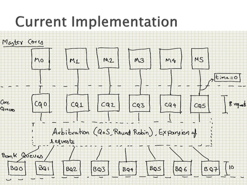
Codes to Improve Accesses
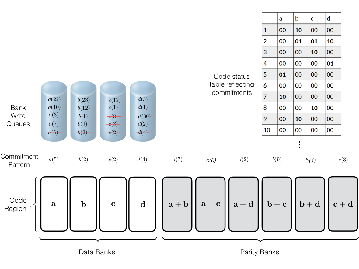
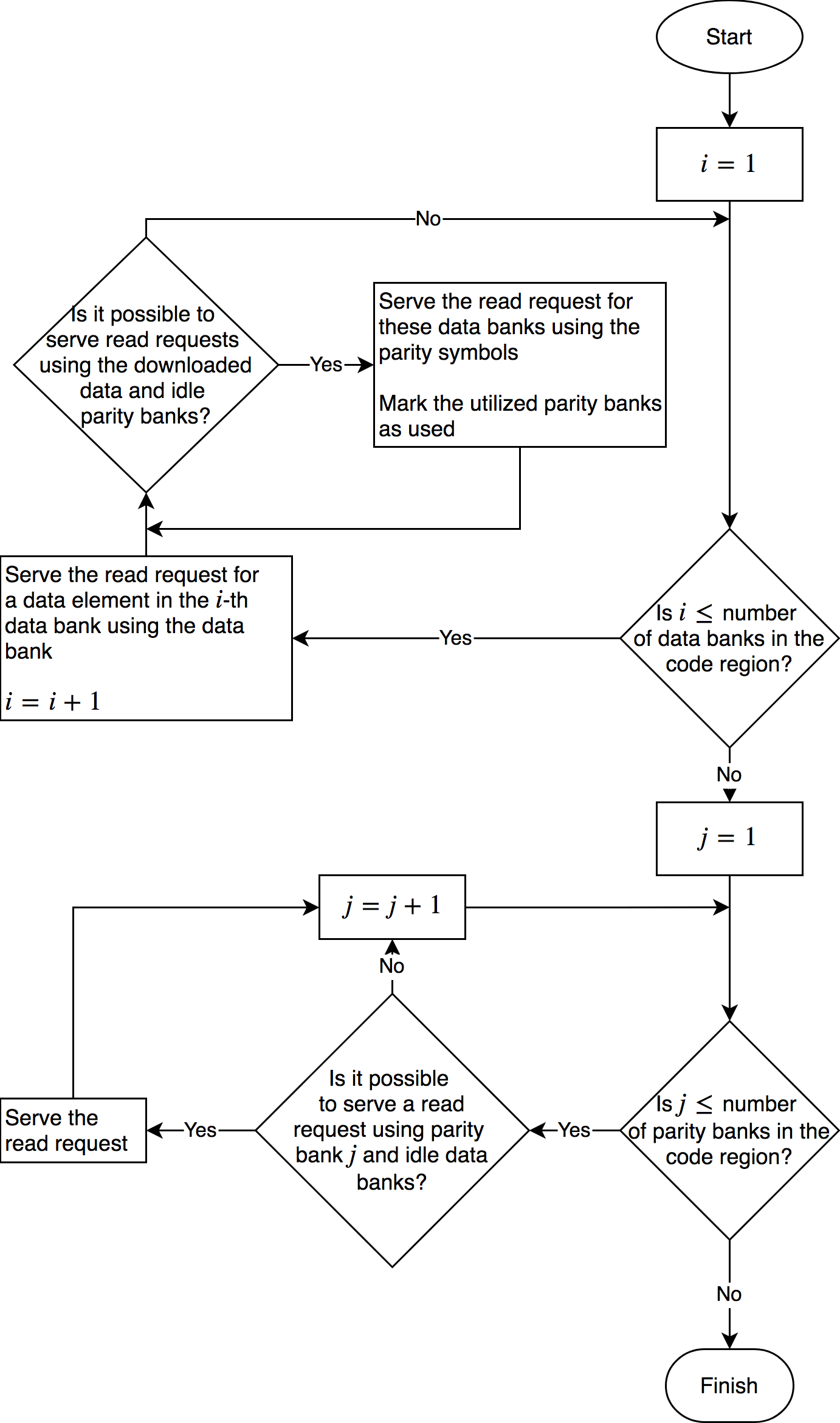
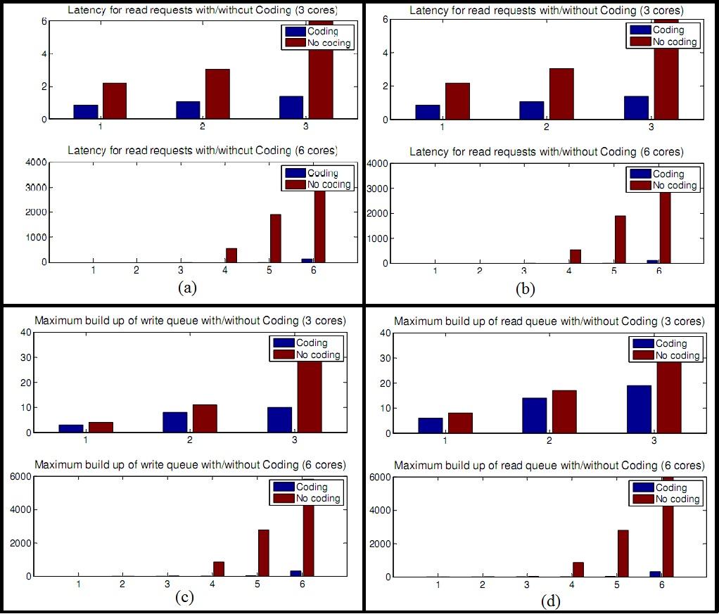
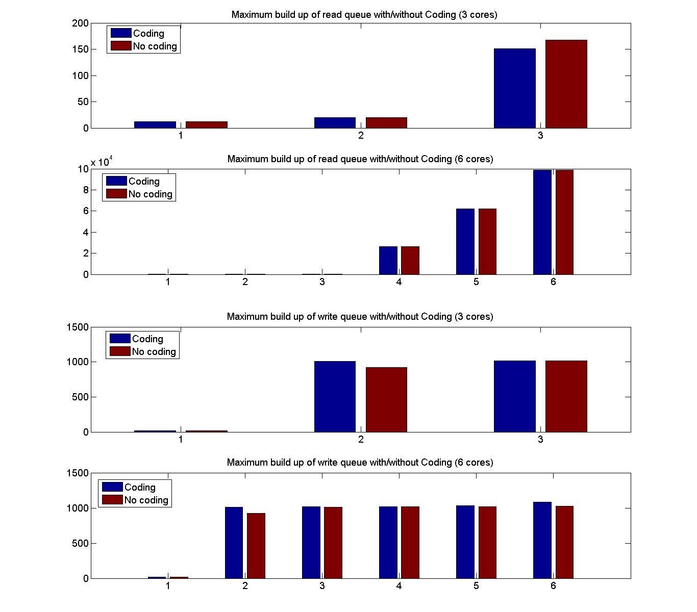
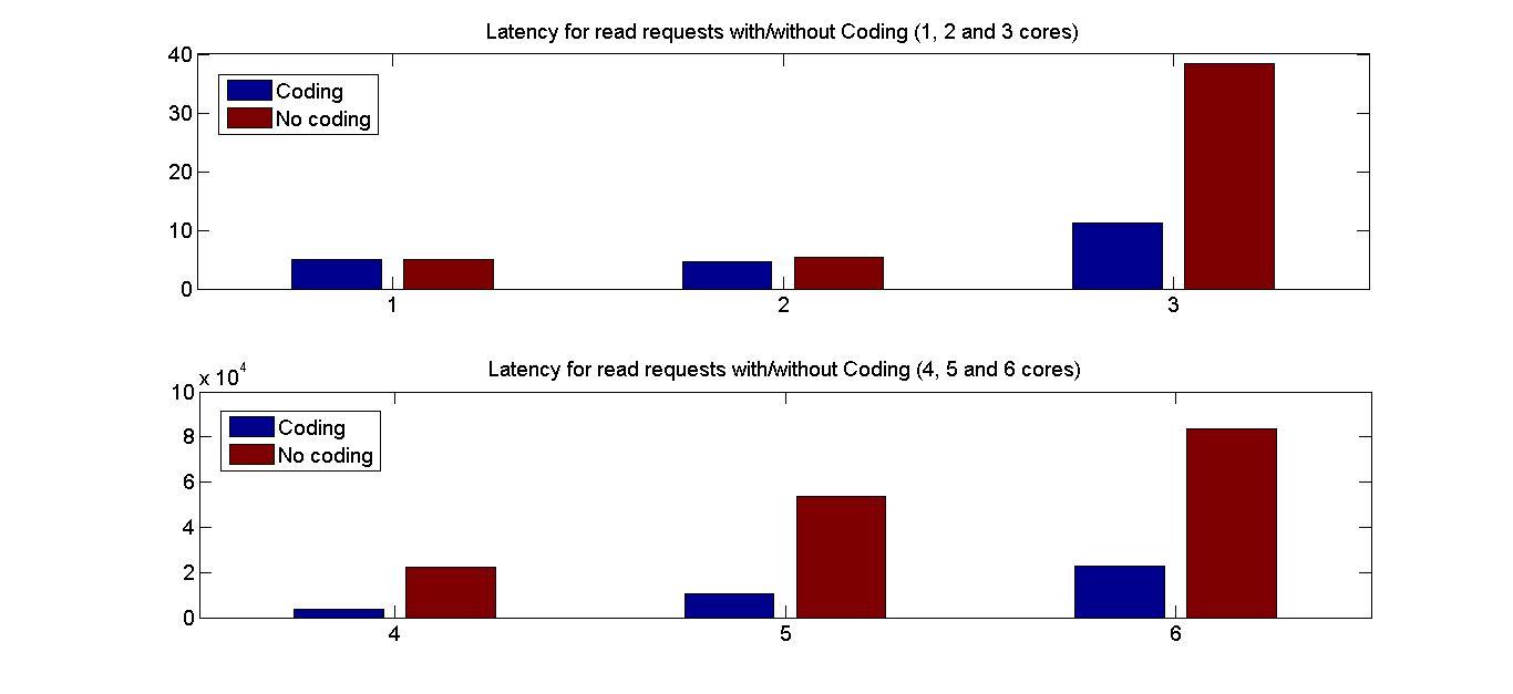
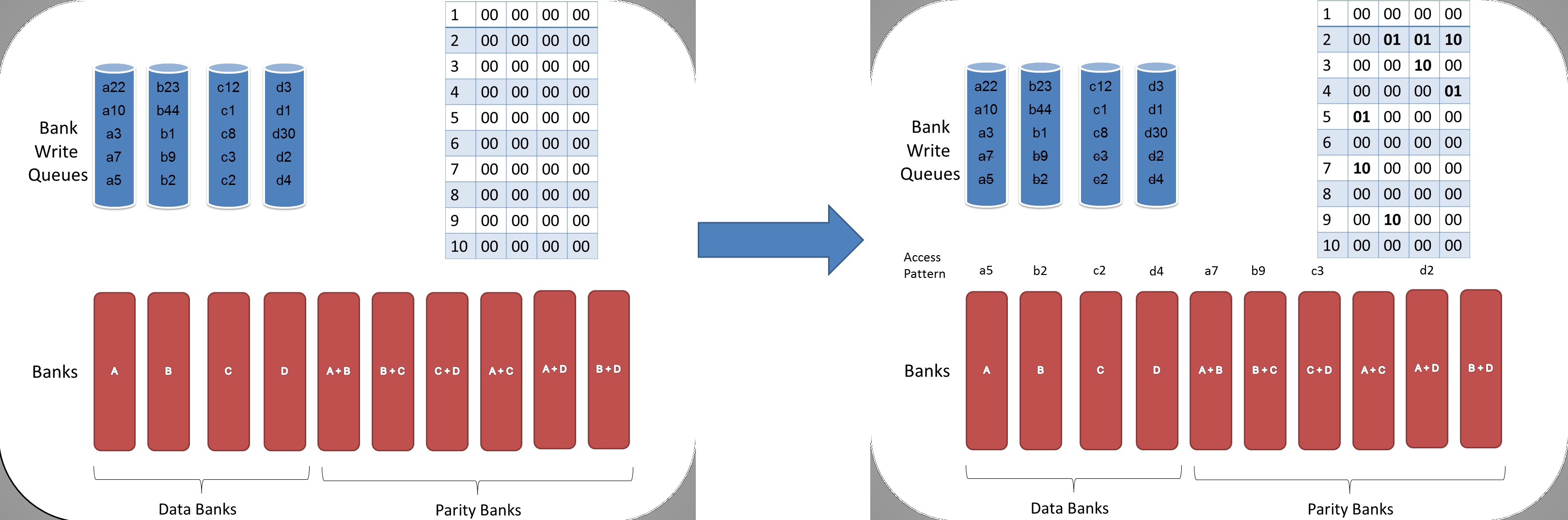
Introducing redundancy into a storage space comprised of single-port
memory banks enables simultaneous memory access. In this section we
propose memory designs that utilize coding schemes which are designed
for access-efficiency. We first define some basic concepts with an
illustrative example and then describe $`3`$ coding schemes in detail.
Coding for memory banks
A coding scheme defines how memory is encoded to yield redundant
storage. The memory structures which store the original memory elements
are known as data banks. The elements of the data banks go through an
encoding process which generates a number of parity banks. The
parity banks contain elements constructed from elements drawn from two
or more data banks. A linear encoding process such as XOR may be used to
minimize computational complexity. The following example further
clarifies these concepts and provides some necessary notation.
Consider a setup with two data banks $`\mathbf{a}`$ and $`\mathbf{b}`$.
We assume that each of the banks store $`L \cdot W`$ binary data
elements1 which are arranged in an $`L \times W`$ array. In
particular, for $`i \in [L] \triangleq \{1,\ldots, L\}`$, $`a(i)`$ and
$`b(i)`$ denote the $`i`$-th row of the bank $`\mathbf{a}`$ and bank
$`\mathbf{b}`$, respectively. Moreover, for $`i \in [L]`$ and
$`j \in [W] \triangleq \{1,\ldots, W\}`$, we use $`a_{i, j}`$ and
$`b_{i, j}`$ to denote the $`j`$-th element in the rows $`a(i)`$ and
$`b(i)`$, respectively. Therefore, for $`i \in [L]`$, we have
Now, consider a linear coding scheme that produces a parity bank
$`\mathbf{p}`$ with $`L'W`$ bits arranged in an $`L' \times W`$ array
such that for $`i \in [L'] \triangleq \{1,\ldots, L'\}`$,
Figure 15 illustrates this coding scheme.
Because the parity bank is based on those rows of the data banks that
are indexed by the set $`[L'] \subseteq [L]`$, we use the following
concise notation to represent the encoding of the parity bank.
MATH
\mathbf{p} = \mathbf{a}([L']) + \mathbf{b}([L']).
Click to expand and view more
In general, we can use any subset
$`\mathcal{S} = \{i_1, i_2,\ldots, i_{L'}\} \subseteq [L]`$ comprising
$`L'`$ rows of data banks to generate the parity bank $`\mathbf{p}`$. In
this case, we have
$`\mathbf{p} = \mathbf{a}(\mathcal{S}) + \mathbf{b}(\mathcal{S})`$, or
style="width:45.0%" />
This illustration is an example parity
design.
Note that we allow for the data banks and parity banks to have different
sizes, i.e. $`L \neq L'`$. This freedom in memory design can be
utilized to reduce the storage overhead of parity banks based on the
underlying application. If the size of a parity bank is smaller than a
data bank, i.e. $`L' < L`$, we say that the parity bank is a shallow
bank. We note that it is reasonable to assume the existence of shallow
banks, especially in proprietary designs of integrated memories in a
system on a chip (SoC).
Note that the size of
shallow banks is a design choice which is controlled by the parameter
$`0 < \alpha \leq 1`$. A small value of $`\alpha`$ corresponds to small
storage overhead. The choice of a small $`\alpha`$ comes at the cost of
limiting parity memory accesses to certain memory ranges. In
Section 13.5 we discuss techniques for
choosing which regions of memory to encode. In scenarios where many
memory accesses are localized to small regions of memory, shallow banks
can support many parallel memory accesses for little storage overhead.
For applications where memory access patterns are less concentrated, the
robustness of the parity banks allows one to employ a design with
$`\alpha = 1`$.
Degraded reads and their locality
The redundant data generated by a coding scheme mitigates bank conflicts
by supporting multiple read accesses to the original data elements.
Consider the coding scheme illustrated in
Figure 15 with a parity bank
$`\mathbf{p} = \mathbf{a}([L']) + \mathbf{b}([L'])`$. In an uncoded
memory system simultaneous read requests for bank $`\mathbf{a}`$, such
as $`a(1)`$ and $`a(5)`$, result in a bank conflict. The introduction of
$`\mathbf{p}`$ allows both read requests to be served. First, $`a(1)`$
is served directly from bank $`\mathbf{a}`$. Next, $`b(5)`$ and $`p(5)`$
are downloaded. $`a(5) = b(5) + p(5)`$, so $`a(5)`$ is recovered by
means of the memory in the parity bank. A read request which is served
with the help of parity banks is called a degraded read. Each degraded
read has a parameter locality which corresponds to the total number of
banks used to serve it. Here, the degraded read for $`a(5)`$ using
$`\mathbf{b}`$ and $`\mathbf{p}`$ has locality $`2`$.
Codes to emulate multi-port memory
We will now describe the code schemes proposed for the emulation of
multi-port memories. Among a large set of possible coding schemes, we
focus on three specific coding schemes for this task. We believe that
these three coding schemes strike a good balance among various
quantitative parameters, including storage overhead, number of
simultaneous read requests supported by the array of banks, and the
locality associated with various degraded reads. Furthermore, these
coding schemes respect the practical constraint of encoding across a
small number of data banks. In particular, we focus on the setup with
$`8`$ memory banks.
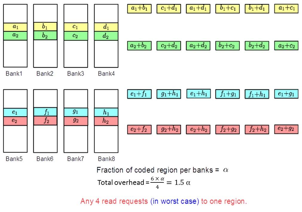
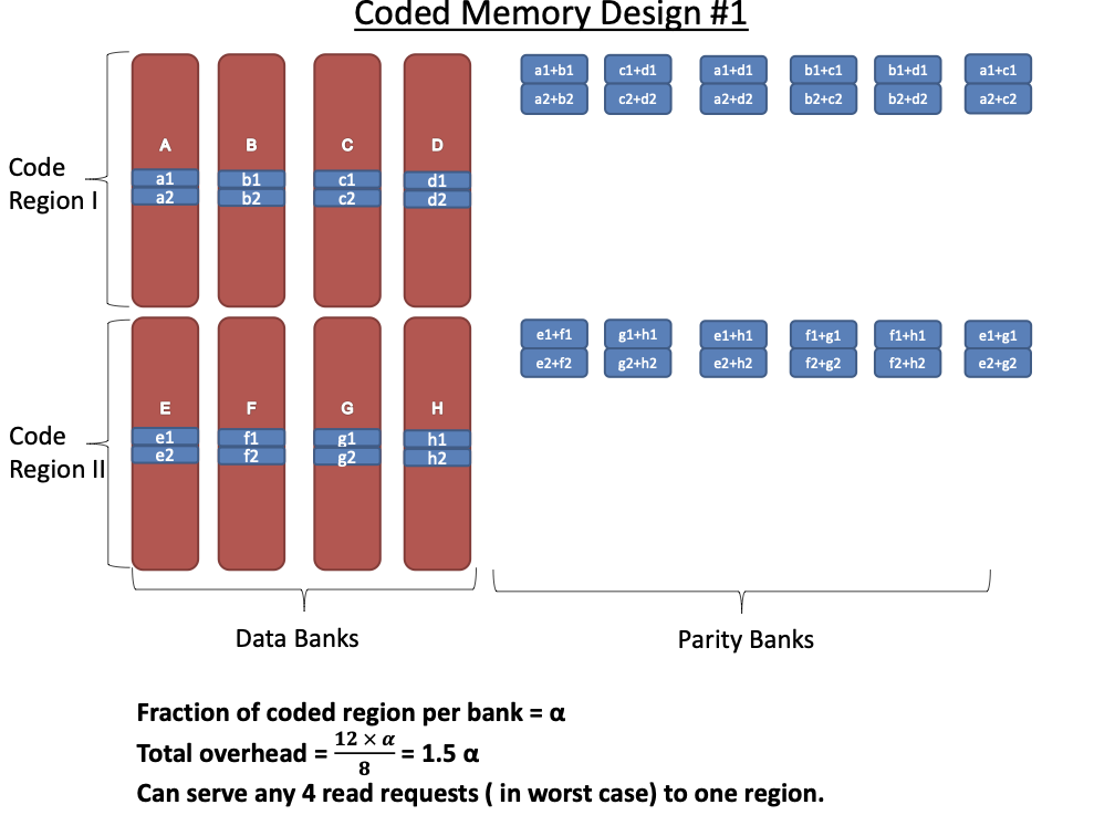
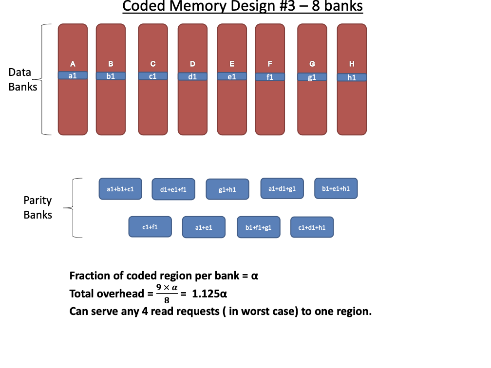
Code Scheme I
This code scheme is motivated from the concept of batch codes which
enables parallel access to content stored in a large scale distributed
storage system. The code scheme involves $`8`$ data banks
$`\{\mathbf{a}, \mathbf{b},\ldots, \mathbf{h}\}`$ each of size $`L`$ and
$`12`$ shallow banks each of size $`L' = \alpha L`$. We partition the
$`8`$ data banks into two groups of $`4`$ banks. The underlying coding
scheme produces shallow parity banks by separately encoding data banks
from the two groups.
Figure 16 shows the resulting memory banks.
The storage overhead of this schemes is $`12\alpha L`$ which implies the
rate2 of the coding scheme is
We now analyze the number of simultaneous read requests that can be
supported by this code scheme.
**Best case analysis: **This code scheme achieves maximum performance
when sequential accesses to the coded regions are issued. During the
best case access, we can achieve up to $`10`$ parallel accesses to a
particular coded region in one access cycle. Consider the scenario when
we receive accesses to the following $`10`$ rows:
Note that we can serve the read requests for the rows
$`\{a(1),b(1),c(1),d(1)\}`$ using the data bank $`\mathbf{a}`$ and the
three parity banks storing $`\{a(1)+b(1), b(1)+c(1),c(1)+d(1)\}`$. The
requests for $`\{a(2),c(2),d(2)\}`$ can be served by downloading
$`b(2)`$ from the data bank $`\mathbf{b}`$ and
$`\{a(2)+d(2), b(2)+d(2),a(2)+c(2)\}`$ from their respective parity
banks. Lastly, in the same memory clock cycle, we can serve the requests
for $`\{c(3), d(3)\}`$ using the data banks $`\mathbf{c}`$ and
$`\mathbf{d}`$.
Pictured here is an illustration of code scheme
I.
Worst case analysis: This code scheme
(cf. Figure 16) may fail to utilize any parity
banks depending on the requests waiting to be served. The worst case
scenario for this code scheme is when there are non-sequential and
non-consecutive access to the memory banks. Take for example a scenario
where we only consider the first four banks of the code scheme. The
following read requests are waiting to be served:
Because none of the requests share the same row index, we are unable to
utilize the parity banks. The worst case number of reads per cycle is
equal to the number of data banks.
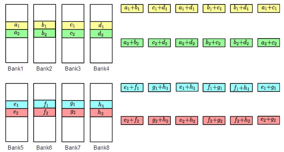
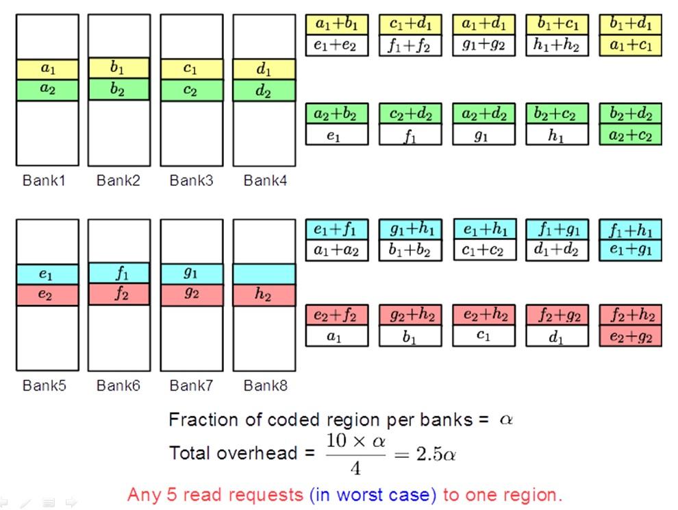
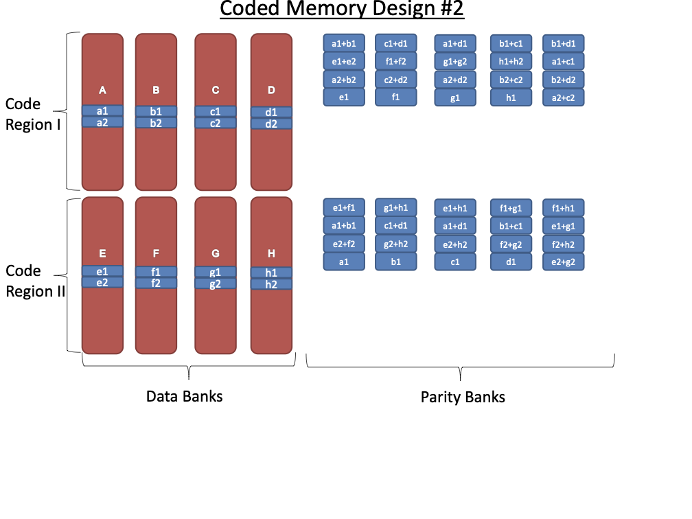
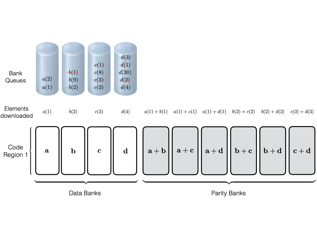
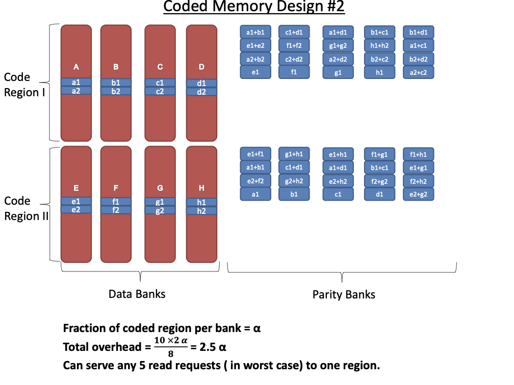
Code Scheme II
Figure 17 illustrates the second code scheme
explored in this paper. Again, the $`8`$ data banks
$`\{\mathbf{a}, \mathbf{b},\ldots, \mathbf{h}\}`$ are partitioned into
two groups containing $`4`$ data banks each. These two groups are then
associated with two code regions. The first code region is similar to
the previous code scheme, as it contains parity elements constructed
from two data banks. The second code region contains data directly
duplicated from single data banks. This code scheme further differs from
the previous code scheme (cf.
Figure 16) in terms of the size and
arrangement parity banks. Even though $`L' = \alpha L`$ rows from each
data bank are stored in a coded manner by generating parity elements,
the parity banks are assumed to be storing $`2\alpha L > L'`$ rows.
For a specific choice of $`\alpha`$, the storage overhead of this scheme
is $`20\alpha L`$ which leads to a rate of
Note that this code scheme can support $`5`$ read accesses per data bank
in a single memory clock cycle as opposed to $`4`$ read requests
supported by the code scheme from
Section 8.2.1. However, this is made possible
at the cost of extra storage overhead. Next, we discuss the performance
of this code scheme in terms of the number of simultaneous read requests
that can be served in the best and worst case.
Pictured here is an illustration of code scheme
II.
**Best case analysis: ** This code scheme achieves the best access
performance when sequential accesses to the data banks are issued. In
particular, this scheme can support up to $`9`$ read requests in a
single memory clock cycle. Consider the scenario where we receive read
requests for the following rows of the data banks:
Here, we can serve $`\{a(1), b(1), c(1), d(1)\}`$ using the data bank
$`\mathbf{a}`$ with the parity banks storing the parity elements
$`\{a(1) + b(1),b(1)+c(1),c(1)+d(1)\}`$. Similarly, we can serve the
requests for the rows $`\{a(2),b(2),d(2)\}`$ using the data bank
$`\mathbf{b}`$ with the parity banks storing the parity elements
$`\{a(2)+d(2), b(2)+d(2)\}`$. Lastly, the request for the rows $`c(2)`$
and $`d(3)`$ is served using the data banks $`\mathbf{c}`$ and
$`\mathbf{d}`$.
**Worst case analysis: **Similar to the worst case in Scheme I, this
code scheme can enable $`5`$ simultaneous accesses in a single memory
clock cycle in the worst case. The worst case occurs when requests are
non-sequential and non-consecutive.
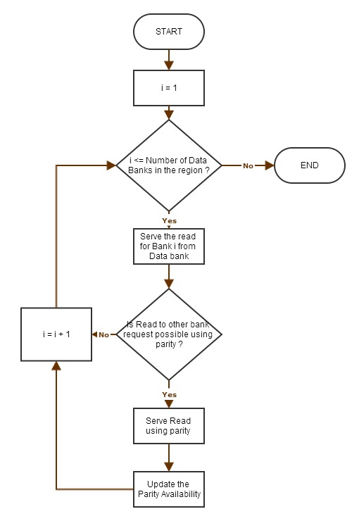
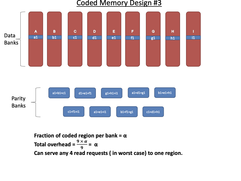
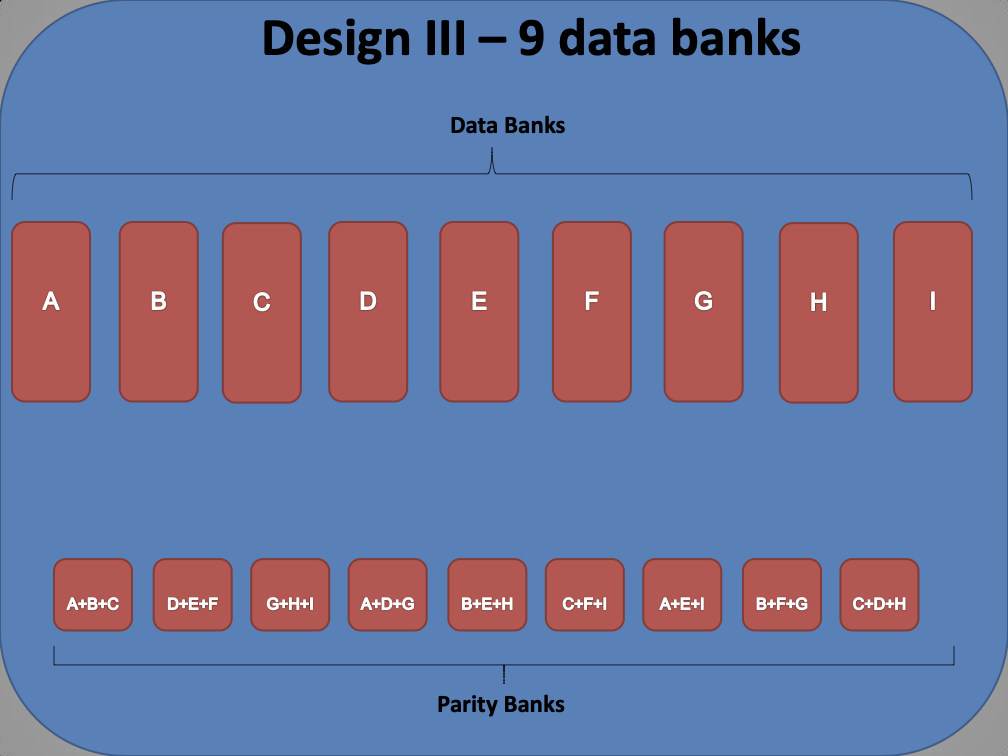
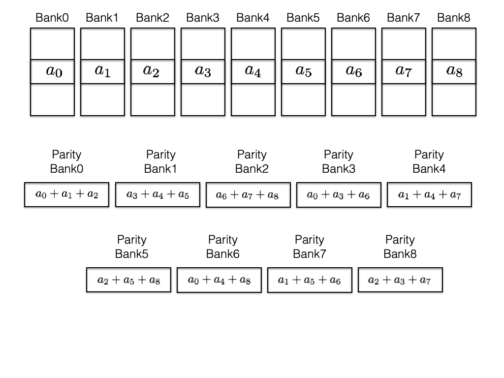
Code Scheme III
The next code scheme we discuss has locality 3, so each degraded read
requires two parity banks to be served. This code scheme works with
$`9`$ data bank
$`\{\mathbf{a}, \mathbf{b},\ldots, \mathbf{h}, \mathbf{z}\}`$ and
generates $`9`$ shallow parity banks.
Figure 18 shows this scheme. The storage
overhead of this scheme is $`9\alpha L`$ which corresponds to the rate
of $`\frac{1}{1 + \alpha}`$. We note that this scheme possesses higher
logical complexity as a result of its increased locality.
This scheme supports $`4`$ simultaneous read access per bank per memory
clock cycle as demonstrated by the following example. Suppose rows
$`\{a(1), a(2), a(3), a(4)\}`$ are requested. $`a(1)`$ can be served
directly from $`\mathbf{a}`$. $`a(2)`$ is served by means of a parity
read and reads to banks $`\mathbf{b}`$ and $`\mathbf{c}`$, $`a(3)`$ is
served by means of a parity read and reads to banks $`\mathbf{d}`$ and
$`\mathbf{g}`$, and $`a(4)`$ is served by means of a parity read and
reads to banks $`\mathbf{e}`$ and $`\mathbf{z}`$.
**Best case analysis: ** Following the analysis similar to code schemes
I and II, the best case number of reads per cycle will be equal to the
number of data and parity banks.
**Worst case analysis: ** Similar to code schemes I and II, the number
of reads per cycle is equal to the number of data banks.
Pictured here is an illustration of code scheme
III.
Note that the coding scheme in
Figure 18 describes a system with $`9`$ data
banks. However, we have set out to construct a memory system with $`8`$
data banks. It is straightforward to modify this code scheme to work
with $`8`$ data banks by simple omitting the final data bank from the
encoding operation.
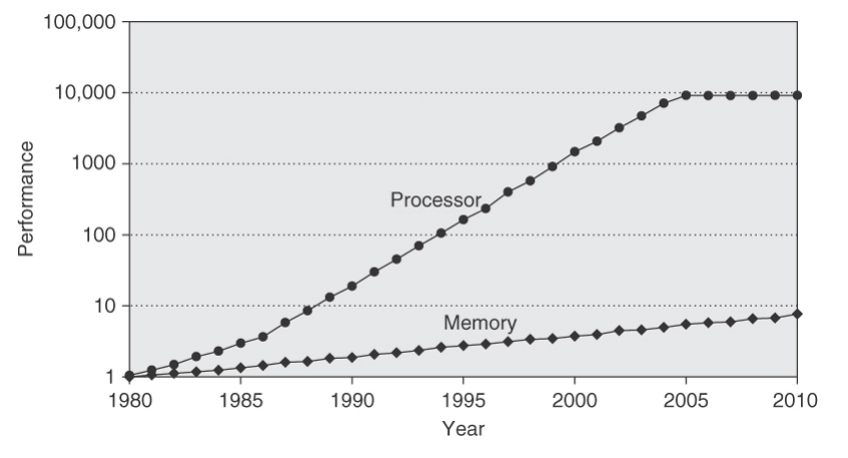
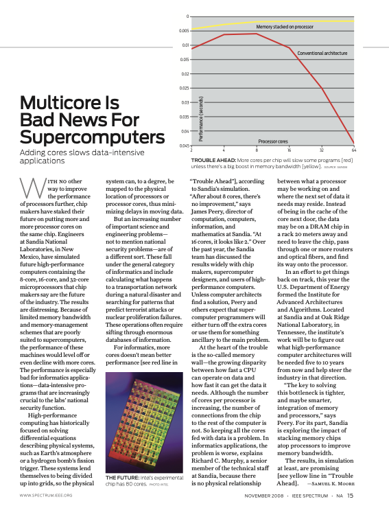
Introduction
Loading and storing information to memory is an intrinsic part of any
computer program. As illustrated in
Figure 19, the past few decades have seen
the performance gap between processors and memory grow. Even with the
saturation and demise of Moore’s law , processing power is expected to
grow as multi-core architectures become more reliable . The end-to-end
performance of a program heavily depends on both processor and memory
performance. Slower memory systems can bottleneck computational
performance. This has motivated computer architects and researchers to
explore strategies for shortening memory access latency, including
sustained efforts towards enhancing the memory hierarchy . Despite these
efforts, long-latency memory accesses do occur when there is a miss in
the last level cache (LLC). This triggers an access to shared memory,
and the processor is stalled as it waits for the shared memory to return
the requested information.
The gap in performance, measured as the difference
in the time between processor memory requests for a single processor and
the latency of a DRAM access .
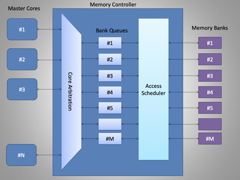
In multi-core systems, shared memory access conflicts between cores
result in large access request queues.
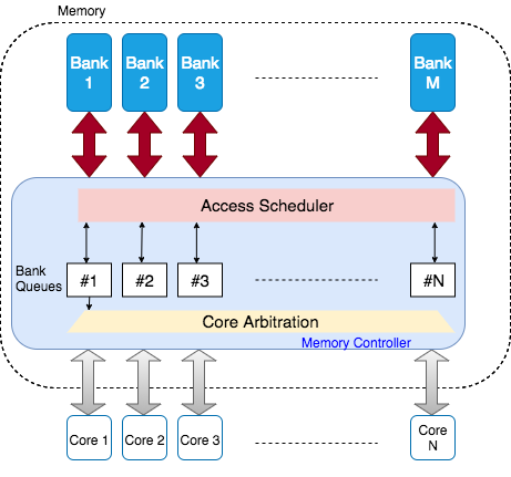
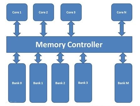
Figure 20 illustrates a general
multi-core architecture. The bank queues are served every memory clock
cycle and the acknowledgement with data is sent back to the
corresponding processor. In scenarios where multiple cores request
access to memory locations in the same bank, the memory controller
arbitrates them using bank queues. This contention between cores to
access from the same bank is known as a bank conflict. As the number
of bank conflicts increases, the resultant increases in memory access
latency causes the multi-core system to slow.
General multi-core architecture with a shared
memory. N processor cores
share a memory consisting of M
banks.
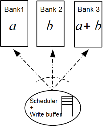
We address the issue of increased latency by introducing a coded memory
design. The main principle behind our memory design is to distribute
accesses intended for a particular bank across multiple banks. We
redundantly store encoded data, and we decode memory for highly
requested memory banks using idle memory banks. This approach allows us
to simultaneously serve multiple read requests intended for a particular
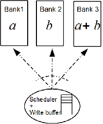
bank. Figure 21 shows this with an example.
Here, Bank 3 is redundant as its content is a function of the content
stored on Banks 1 and 2. Such redundant banks are also referred to as
parity banks. Assume that the information is arranged in $`L`$ rows in
two first two banks, represented by $`[a(1),\ldots, a(L)]`$ and
$`[b(1),\ldots, b(L)]`$, respectively. Let $`+`$ denote the XOR
operation, and additionally assume that the memory controller is capable
of performing simple decoding operations, i.e. recovering $`a(j)`$
from $`b(j)`$ and $`a(j) + b(j)`$. Because the third bank stores $`L`$
rows containing $`[a(1) + b(1),\ldots, a(L) + b(L)]`$, this design
allows us to simultaneously serve any two read requests in a single
memory clock cycle.
style="width:30.0%" />
Here the redundant memory in Bank 3 enables
multiple read accesses to Bank 1 or 2. Given two read requests {a(i), a(j)}
directed to Bank 1, we can resolve bank
conflict by reading a(i) directly from Bank 1
and acquiring a(j)
with two reads from Bank 2 and Bank 3. b(j) and a(j) + b(j)
are read from Bank 2 and Bank 3, and a(j) is recovered because
a(j) = b(j) + a(j) + b(j).
Hybrid memory designs such as the one in
Figure 21 have additional requirements in
addition to serving read requests. The presence of redundant parity
banks raises a number of challenges while serving write requests. The
memory overhead of redundant memory storage adds to the overall cost of
such systems, so efforts must be made to minimize this overhead.
Finally, the heavy memory access request rate possible in multi-core
scenarios necessitates sophisticated scheduling strategies to be
performed by the memory controller. In this paper we address these
design challenges and evaluate potential solutions in a simulated memory
environment.
**Main contributions and organization: **In this paper we systematically
address all key issues pertaining to a shared memory system that can
simultaneously service multiple access requests in a multi-core setup.
We present all the necessary background on realization of multi-port
memories using single-port memory banks along with an account of
relevant prior work in
Section 7. We then present the main contributions of
the paper which we summarize below.
We focus on the design of the storage space in
Section 8. In particular, we employ three
specific coding schemes to redundantly store the information in memory
banks. These coding schemes, which are based on the literature on
distributed storage systems , allow us to realize the functionality of
multi-port memories from single port memories while efficiently
utilizing the storage space.
We present a memory controller architecture for the proposed coding
based memory system in
Section 13. Among other issues, the memory
controller design involves devising scheduling schemes for both read
and write requests. This includes careful utilization of the
redundancy present in the memory banks while maintaining the validity
of information stored in them.
Focusing on applications where memory traces might exhibit favorable
access patterns, we explore dynamic coding techniques which improve
the efficiency of our coding based memory design in
Sections 13.5.
Finally, we conduct a detailed evaluation of the proposed designs of
shared memory systems in
Section 14. We implement our
memory designs by extending Ramulator, a DRAM simulator . We use the
gem5 simulator to create memory traces of the PARSEC benchmarks
which are input to our extended version of Ramulator. We then observe
the execution-time speedups our memory designs yield.
Code Design Objectives
The following objects inspired our proposed memory system:
Read access : 4 per bank in one cycle
Write access : 2 per bank in one cycle
Shared Memory size 8 kB - 256 kB
Number of Banks : 8
Memory overhead : 15$`\%`$
Parity banks : 5 or 6 shallow banks for code storage
Background and Related Work
Emulating multi-port memories
Multi-port memory systems are often considered to be essential for
multi-core computation. Individual cores may request memory from the
same bank simultaneously, and absent a multi-port memory system some
cores will stall. Multi-port memory systems have significant design
costs. Complex circuitry and area costs for multi-port bit-cells are
significantly higher than those for single-port bit-cells . This
motivates the exploration of algorithmic and systematic designs that
emulate multi-port memories using single-ported memory banks . Attempts
have been made to emulate multi-port memory using replication based
designs , however the resulting memory architectures are very large.
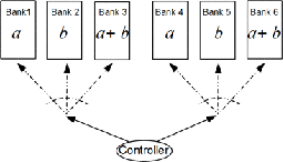
Read-only Support
Replication-based designs are often proposed as a method for multi-port
emulation. Suppose that a memory design is required to support only read
requests, say $`r`$ read requests per memory clock cycle. A simple
solution is storing $`r`$ copies of each data element on $`r`$ different
single-port memory banks. In every memory clock cycle, the $`r`$ read
requests can be served in a straightforward manner by mapping all read
request to distinct memory banks (see
Figure 22). This way, the
$`r`$-replication design completely avoids bank conflicts for up to
$`r`$ read request in a memory clock cycle.
If we compare the
memory design in
Figure 22 with that of
Figure 21, we notice that both designs can
simultaneously serve $`2`$ read requests without causing any bank
conflicts. Note that the design in
Figure 21 consumes less storage space as
it needs only $`3`$ single-port memory banks while the design in
Figure 22 requires $`4`$ single-port
memory banks. However, the access process for the design in
Figure 21 involves some computation. This
observation raises the notion that sophisticated coding schemes allow
for storage efficient designs compared to replication based methods .
However, this comes at the expense of increased computation required for
decoding.
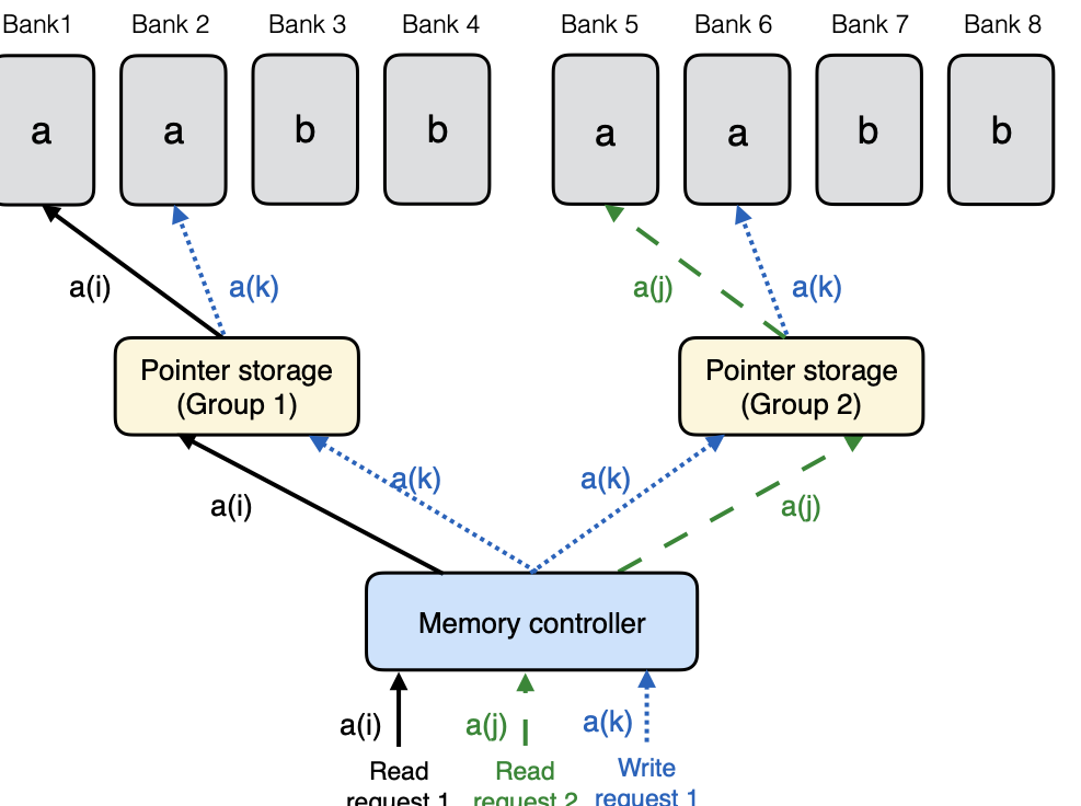
style="width:42.5%" />
A 2-replication
design which supports 2 read requests
per bank. In this design, the data is partitioned between two banks
a = [a(1), …, a(L)]b = [b(1), …, b(L)]
and duplicated. style="width:60.0%" />
A 4-replication
based design to support r = 2
read requests and w = 1 write
requests. Both collections of information elements a = [a(1), …, a(L)]
and b = [b(1), …, b(L)]
are replicated to obtain r ⋅ (w + 1) = 4 single-port
memory banks. These banks are then partitioned into r = 2 disjoint groups, Banks 1 – 4 and
Banks 5 – 8. The pointer storage is required to ensure
all read requests are not served stale symbols. As shown in the
illustration, the write request is served to two of the a banks to ensure that the
fresh a(k) may be
served during any future cycle.
Read and Write Support
A proper emulation of multi-port memory must be able to serve write
requests. A challenge that arises from this requirement is tracking the
state of memory. In replication-based designs where original data banks
are duplicated, the service of writes requests results in differences in
state between the original and duplicate banks.
Replication-based solutions to the problems presented when supporting
write requests involve creating yet more duplicate banks. A
replication-based multi-port memory emulation that simultaneously
supports $`r`$ read requests and $`w`$ write requests requires a
$`r\cdot(w + 1)`$ replication scheme, where $`r\cdot(w+1)`$ copies of
each data element are stored on $`r\cdot(w + 1)`$ different single-port
memory banks. We illustrate this scheme for $`r = 2`$ and $`w = 1`$ in
Figure 23. As in previous
illustrations, we have two groups of symbols
$`\mathbf{a} = [a(1),\ldots, a(L)]`$ and
$`\mathbf{b} = [b(1),\ldots, b(L)]`$. We store $`4`$ copies each of
data elements $`\mathbf{a}`$ and $`\mathbf{b}`$ and partition the banks
into $`r = 2`$ disjoint groups. Each group contains $`(w + 1) = 2`$
memory banks. An additional storage space, the pointer storage, is
required to keep track the state of the data in the banks.
Storage-efficient emulation of multi-port memories
As described in
Section 7.1, introducing redundancy to
systems which use single-port memory banks allows such systems to
emulate the behavior of multi-port banks. Emulating multi-port read and
write systems is costly (cf.
Section 7.1.2). A greater number of single-port
memory banks are needed, and systems which redundantly store memory
require tracking of the various versions of the data elements present in
the memory banks. Furthermore, as write requests are served the elements
stored across redundant banks temporary differ. This transient
inconstancy between redundant storage complicates the process of
arbitration.
We believe that various tasks that arise in the presence of write
requests and contribute to computational overhead of the memory design,
including synchronization among memory banks and complicated
arbitration, can be better managed at the algorithmic level. Note that
these tasks are performed by the memory controller. It is possible to
mitigate the effect of these tasks on the memory system by relying on
the increasing available computational resources while designing the
memory controller. Additionally, we believe that large storage overhead
is a more fundamental issue that needs to be addressed before multi-port
memory emulation is feasible. In particular, the large replication
factor in a naive emulation creates such a large storage overhead that
the resulting area requirements of such designs are impractical.
Another approach arises from the observation that some data banks are
left unused during arbitration in individual memory cycles, while other
data banks receive multiple requests. We encode the elements of the data
banks using specific coding schemes to generate parity banks. Elements
drawn from multiple data banks are encoded and stored in the parity
banks. This approach allows us to utilize idle data banks to decode
elements stored in the parity banks in service of multiple requests
which target the same data bank. We recognize that this approach leads
to increased complexity at the memory controller. However, we show that
the increase in complexity can be kept within an acceptable level while
ensuring storage-efficient emulation of multi-port memories.
Related work
Coding theory is a well-studied field which aims to mitigate the
challenges of underlying mediums in information processing systems .
The field has enabled both reliable communication across noisy channels
and reliability in fault-prone storage units. Recently, we have
witnessed intensive efforts towards the application of coding theoretic
ideas to design large scale distributed storage systems . In this
domain, the issue of access efficiency has also received attention,
especially the ability to support multiple simultaneous read accesses
with small storage overhead . In this paper, we rely on such coding
techniques to emulate multi-port memories using single-port memory
banks. We note that the existing work on batch codes focuses only on
read requests, but the emulation of multi-port memory must also handle
write requests.
Coding schemes with low update complexity that can be implemented at the
speed memory systems require have also been studied . Our work is
distinguished from the majority of the literature on coding for
distributed storage, because we consider the interplay between read and
write requests and how this interplay affects memory access latency.
The work which is closest to our solution for emulating a multi-port
memory is by Iyer and Chuang , where they also employ XOR based coding
schemes to redundantly store information in an array of single-port
memory banks. However, we note that our work significantly differers
from as we specifically rely on different coding schemes arising under
the framework of batch codes . Additionally, due to the employment of
distinct coding techniques, the design of memory controller in our work
also differs from that in .
Memory systems work hard to keep up with access requests from cores.
Growing computer sizes, heterogeneous systems and increasing level of
integration has increased more. Performance focused systems use
enhancements like multi-port memories to increase the access capacity.
However, they come with a cost in terms of area, complexity and cost of
redesign and rebuilding a system. In this paper, we explore a
mathematical solution to the problem where we explore an efficient
memory storage and reterival mechanism for efficent access. We first
analyze the request pattern of general memory controller and a
application-specific memory controller.
We then provide a mathematical approach to storing the data in specific
way to achieve higher access rate. We call this specific way of storing
the memory as Algorithmic Memory. We discuss methods to design codes and
provide example designs for 8 bank memory systems.
At last, we analyze and compare the improvement of coded memory with
general memory. We present a significant improvement in critical word
read and write latency with coded memory. We also provide intuitions
derived from this analysis which can help the system designers to
efficiently use Algorithmic memory implementation.
The copyright of this content belongs to the respective researchers. We deeply appreciate their hard work and contribution to the advancement of human civilization.
It is possible to work with data elements over larger
alphabets/finite fields. However, assuming data elements to be
binary suffices for this paper as only work with coding schemes
defined over binary field. ↩︎
The information rate is a standard measure of redundancy of a
coding scheme ranging from $`0`$ to $`1`$, where $`1`$ corresponds
to the most efficient utilization of storage space. ↩︎