BRISC-V An Open-Source Toolbox for Exploring RISC-V Architecture Design Spaces
📝 Original Paper Info
- Title: BRISC-V An Open-Source Architecture Design Space Exploration Toolbox- ArXiv ID: 1908.09992
- Date: 2019-08-28
- Authors: Sahan Bandara, Alan Ehret, Donato Kava and Michel A. Kinsy
📝 Abstract
In this work, we introduce a platform for register-transfer level (RTL) architecture design space exploration. The platform is an open-source, parameterized, synthesizable set of RTL modules for designing RISC-V based single and multi-core architecture systems. The platform is designed with a high degree of modularity. It provides highly-parameterized, composable RTL modules for fast and accurate exploration of different RISC-V based core complexities, multi-level caching and memory organizations, system topologies, router architectures, and routing schemes. The platform can be used for both RTL simulation and FPGA based emulation. The hardware modules are implemented in synthesizable Verilog using no vendor-specific blocks. The platform includes a RISC-V compiler toolchain to assist in developing software for the cores, a web-based system configuration graphical user interface (GUI) and a web-based RISC-V assembly simulator. The platform supports a myriad of RISC-V architectures, ranging from a simple single cycle processor to a multi-core SoC with a complex memory hierarchy and a network-on-chip. The modules are designed to support incremental additions and modifications. The interfaces between components are particularly designed to allow parts of the processor such as whole cache modules, cores or individual pipeline stages, to be modified or replaced without impacting the rest of the system. The platform allows researchers to quickly instantiate complete working RISC-V multi-core systems with synthesizable RTL and make targeted modifications to fit their needs. The complete platform (including Verilog source code) can be downloaded at https://ascslab.org/research/briscv/explorer/explorer.html.💡 Summary & Analysis
This paper introduces an open-source platform for designing and exploring RISC-V-based single and multi-core systems. The platform comprises modular, parameterized Verilog modules that allow researchers to quickly instantiate complete working RISC-V multi-core systems and make targeted modifications as needed. Key features include a web-based system configuration GUI, a RISC-V assembly simulator, and a compiler toolchain for bare-metal execution.The primary challenge addressed is the difficulty in designing complex multi-core processor systems due to numerous interdependent design decisions that impact performance subtly. The platform provides flexibility by allowing users to explore various configurations of cores with different pipeline depths, cache sizes, associativities, memory subsystems, and on-chip networks.
Key achievements include a set of five-, seven-stage pipelined processors, and an out-of-order execution core. These designs enable researchers to quickly test different micro-architectural features and evaluate their performance under varying conditions. The platform supports extensive customization through parameterization and modularity, enabling users to optimize for specific use cases.
This work is significant because it lowers the barrier to entry for multi-core system design research. It facilitates rapid prototyping and experimentation with complex systems, which can lead to the discovery of new architectural optimizations or validation of existing ones.
📄 Full Paper Content (ArXiv Source)
The five stage processor is implemented by using the base modules from the single cycle processor as a starting point and adding pipeline registers between the combinational fetch, decode, execute, memory and writeback modules. The single cycle control logic module is wrapped with additional logic to support the stall and bypass signals needed for pipelining. Introducing multiple instructions in flight demonstrates how hazard resolution must consider bypassing, stalling, and pipeline flushing.
Pipelining allows for a higher clock frequency; however, NOPs are still inserted between synchronous memory operations because there is no pipeline register between the address input and data output of the memory interfaces. Asynchronous memories must still be used to avoid NOPs between instruction fetches. Note, however, that the addition of pipeline stages allows some synthesis tools to implement an asynchronous main memory (without caches) in FPGA BRAM. The five-stage pipelined processor has two variants. The first uses only pipeline stalls and flushes when a pipeline hazard is detected. The second implements data forwarding to avoid stalls for most hazards. Stalling and forwarding logic is wrapped around the base control unit used in the single cycle core. A multiplexer is wrapped around the decode logic to output forwarded data when needed. Wrapping the base modules to build the five stage pipeline maximizes IP reuse and allows for user base module customizations to be carried through their core design space.
 />
/>
Introduction
Designing, building, and testing multi-core, many-core and even single-core processor systems is a difficult and time consuming task. Designers are faced with numerous design decisions that, when taken as a whole, impact performance in subtle ways. With the ever increasing size and complexity of multi-core and many-core systems, the time and effort needed for development is quickly raising the barrier to entry for design space exploration and research. This growing obstacle to multi-core system design creates a need for a flexible micro-architecture design space exploration platform. However, there are many challenges involved with creating such a platform. Salient research questions related to creating such a platform include: (1) What aspects of a multi-core system are relevant to micro-architecture design space exploration? (2) How can a design space exploration platform provide ease of use and rapid exploration while maintaining the speed and accuracy of FPGA-based emulation? (3) How can the size of the design space covered by a platform be maximized to provide support for a wide range of systems and research?
To address these questions and challenges, we present an open-source platform for RISC-V multi-core system micro-architecture design space exploration. The key components of this platform are:
-
A modular, parameterized, synthesizable multi-core RISC-V hardware system written in Verilog.
-
A RISC-V toolchain to compile a user’s code for bare-metal execution on the hardware system.
-
A RISC-V assembly simulator to test a user’s software independently of the hardware system.
-
A hardware system configuration graphical user interface to visualize and generate multi-core hardware systems.
The name of the platform is withheld to maintain anonymity.
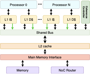
Current research that would benefit from fast micro-architecture design space exploration ranges from the development of efficient network on-chip (NoC) to cache timing side channel elimination to heterogeneous or adaptive architecture design . Indeed, there is still active research related to every subsystem in a multi-core design. As such, our platform supports design space exploration for: (1) RISC-V cores, with various pipeline depths and configurations; (2) the cache subsystem with user selectable sizes and associativities; (3) a main memory subsystem with support for on-chip block RAM (BRAM) or off-chip memory; and (4) a parameterized on-chip network supporting a variety of router designs and routing algorithms.
The hardware system is written in synthesizable Verilog with no vendor specific IP blocks. This implementation enables RTL simulation, in addition to the fast FPGA-based emulation necessary for large, yet accurate, design space exploration. Parameterization and modularity allow for rapid changes to the design of the system. Individual modules (e.g. core pipeline stages or cache replacement policies) as well as whole subsystems (e.g. core, cache or NoC designs) can be customized or replaced independently of each other. This allows users to make changes to their relevant systems without the need to modify or understand implementation details of other aspects of the system. The platform provides multiple implementations of core, cache, memory and NoC subsystems for users to choose from. Parameterized modules allow users to quickly change settings of the system, such as cache size, cache associativity, or number of cores. Such parameters enable the fine tuning of a micro-architecture after the appropriate hardware modules have been selected.
The software tools included in the platform facilitate rapid design space exploration by streamlining the platform work flow. Including the necessary toolchain allows users to develop software for their design space exploration quickly and run it on a variety of system configurations. The platform’s RISC-V assembly simulator can be used to create a golden model of program execution and fine tune software before testing it on the hardware system. These golden models can accelerate debugging efforts by providing an expected execution flow. The hardware system configuration GUI allows users to select core types and features, cache sizes, and associativities, bus-based or NoC- based interconnects, among many other parameters. Visualizations of the configuration promptly give users an understanding of their system. Users can use the GUI to generate an RTL implementation of the system, allowing them to easily make and visualize changes, before producing a new design. The modularity that comes with support for interchangeable core, cache, memory, and NoC subsystems (and their internal modules) enables a wide breadth of design space for exploration, without any RTL modifications to the base platform. In order to maximize the explorable design space, every aspect of the platform is open-source. Users looking to expand the number of supported subsystems or add experimental features can do so by modifying or extending the Verilog RTL of the base system.
The use of RISC-V, an open ISA that is freely available, adds additional possibilities for design space exploration with its modular nature and numerous extension specifications . Users can add custom instruction set extensions to support experimental architecture features or custom hardware accelerators. The openness and the option for custom extensions makes RISC-V an excellent ISA for design space exploration. This platform uses version 2.2 of the RISC-V User-Level ISA
The complete platform (including Verilog source code) can be downloaded at https://ascslab.org/research/briscv/explorer/explorer.html .
Main memory and Network-on-chip
The main memory interface decouples the cache subsystem and the main memory. Users have the option to use any of the provided main memory subsystems: (1) unified or separate asynchronous instruction and data memory, (2) unified or separate synchronous instruction and data memory, or (3) off-chip memory controller.
Connecting the main memory interface to an off-chip memory controller enables large main memories. Using off-chip memory is useful when a system needs more memory than is available on a given FPGA. Currently the platform includes a simple off-chip SRAM memory controller; other device specific memory controllers can easily be added. The interface also supports connections to an on-chip network, which, coupled with the ability to configure the size of main memory on a per node basis, enables uniform and non-uniform distributed memory systems.
On-Chip Network
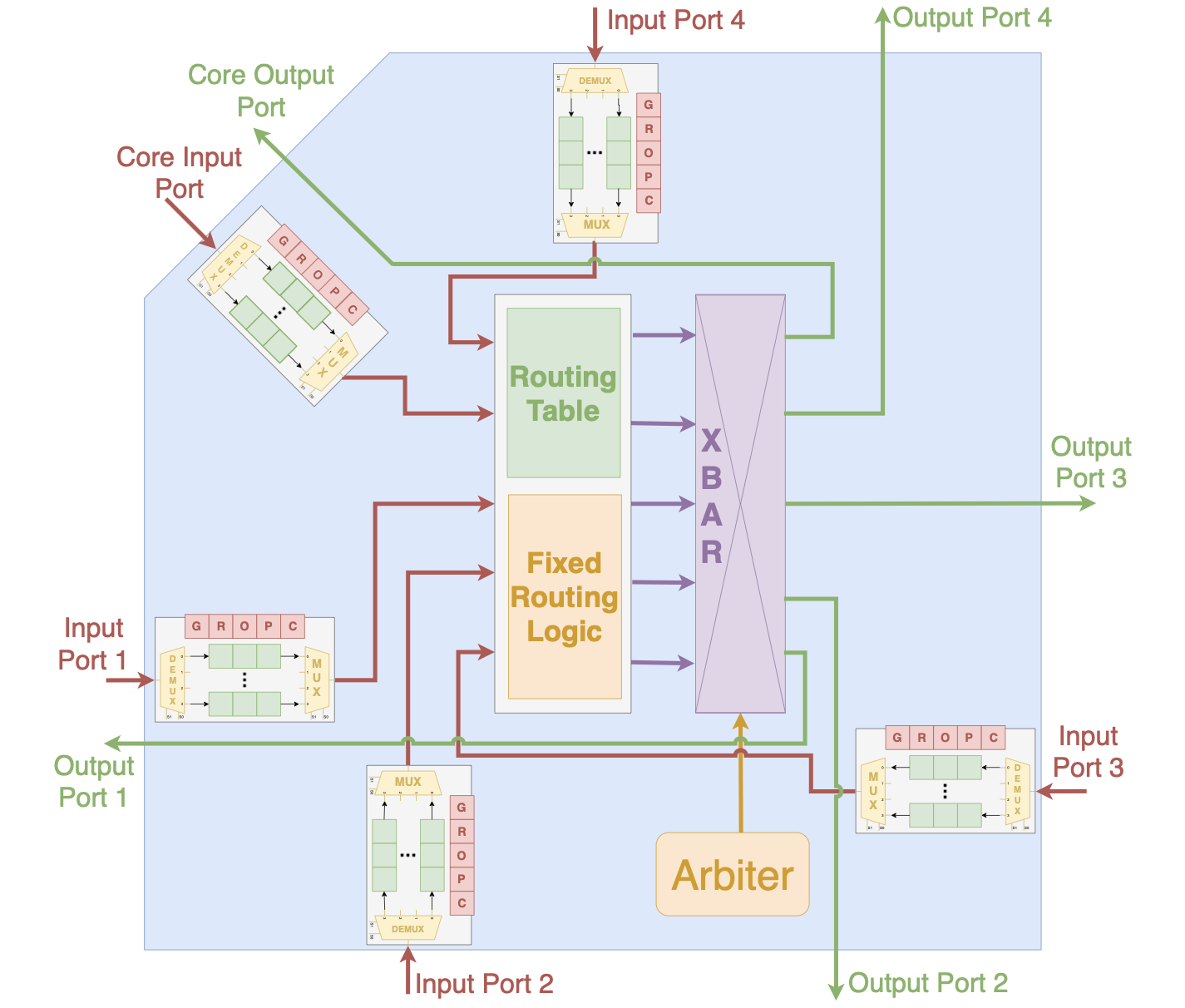
The platform’s on-chip network works with the memory subsystem to implement a variety of multi-core architectures. The NoC provides a number of configuration options, enabling the user to explore different network topologies and optimize the resource usage and performance of the system. The network can be configured to explore different combinations of: 1) flow control, 2) routing algorithms, and 3) network topologies. The NoC router is fully parameterized 2.
Routers in the NoC can be configured as buffered or buffer-less routers. The routers support oblivious routing algorithms using fixed logic or configurable routing tables. Fixed logic is implemented for Dimension Order Routing. Programmable routing tables enable different routing algorithms with changes to the routing table entries. A wide range of network topologies can be be implemented by configuring the number of input ports, output ports and routing table contents of the routers. Routers included in the platform are conventional virtual channel routers. There are single cycle and pipelined variants of the routers. Users can configure different parameters such as number of input/output ports, virtual channels per port, virtual channel depth to tune the performance and resource usage of the on-chip network opening a rich design space for exploration. The on-chip network is based on the NoC included with the Heracles system .
 />
/>
Hardware Configuration GUI
The hardware system configuration application is a graphical application that allows users to configure a hardware system to meet their specification. The application runs in a web browser, allowing users to run it on Windows, Linux, or Mac.
With the hardware configuration system users can (1) select their desired core type and features; (2) include a cache subsystem, if desired, and select its parameters; (3) choose a main memory subsystem, e.g. on-chip, off-chip, unified or separate instruction and data memories; and (4) choose NoC configuration options including number of routers, router topology, and router scheme.
Figure 3 shows a screenshot of the application. On the left are menu and parameter entry text boxes. A block diagram of the configured system is shown on the right of the application window. Selecting different menu options opens different parameter selection tabs. The five core types currently included are 1) single cycle, 2) five-stage pipeline with stall on hazard, 3) five-stage pipeline with data forwarding, 4) seven-stage pipeline with forwarding, and 5) pipelined Out-Of-Order. As the processor cores gain complexity, so do their parameters. The cores are built off of one another, with each core serving as the starting point for the next more complex core. Each new implementation supports the previous processor’s parameters, in addition to any new required parameters. If on-chip main memory is selected, it can be initialized with the “PROGRAM” parameter. This parameter points to a Verilog Memory Hex file that is output by the provided compiler toolchain described in Section 21.3.
After a user has configured the system, clicking “Generate and download” will download the configured RTL and selected binary from the application. Note that the application is run in a web browser but the entire application can also be local to a user’s machine. No internet connection is required to use the configuration GUI. The use of “Download” here refers to the fact that the browser is oblivious to the application’s origin. Running the hardware configuration GUI in a browser enables researchers, students and teachers to use it locally on a platform of their choice or host it on a server for users to access remotely. Hosting the configuration GUI on a server could simplify its use in a classroom environment.
Platform Overview
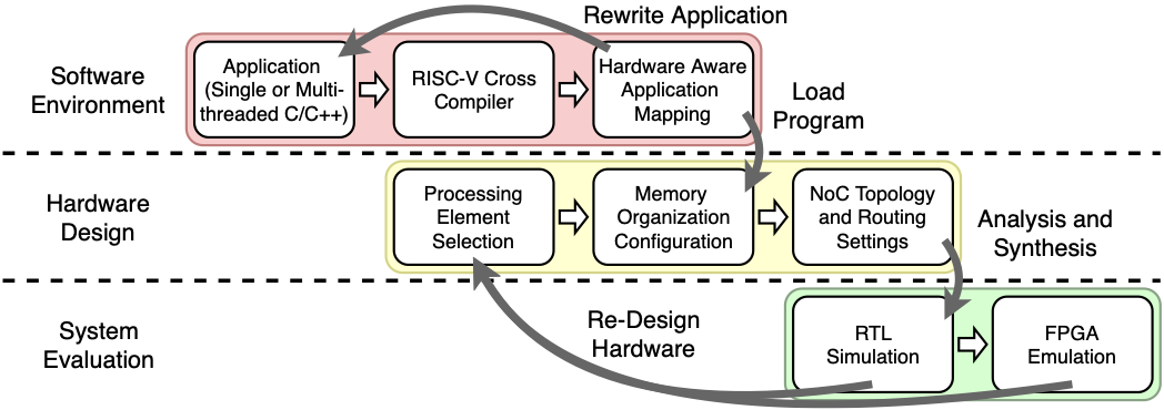
A typical workflow in the platform (shown in Figure 4) starts with developing the software application to be run on the hardware system. Software is compiled with either the GNU or LLVM compiler toolchain for RISC-V. The included compiler scripts support simple multi-processing and multi-threading environments.
After developing the application, users can determine performance requirements as well as power and area constraints. Given the system requirements, a user can begin setting parameters for the core, cache, memory and NoC subsystems. Users can set these parameters with the hardware configuration GUI discussed in Section 21.1. Users requiring a small processor to handle embedded applications might select a small single cycle core with a simple BRAM memory, while a user developing a large distributed multi-core system could opt for the more complex pipelined or out-of-order cores, with large caches and a memory controller for off-chip memory. Users developing a system for a single application can optimize the cache subsystem by selecting line size, associativity, and number of line values best suited to the memory access pattern of the application. For instance, if the application has high spatial locality, then a larger line size can be selected. If users are designing a large many-core processor they can experiment with different NoC topologies and routing algorithms to determine which one gives the best performance for their constraints.
The test benches included in the hardware system can be used to simulate the processing system and verify that the user’s program executes correctly. Tests for the sample programs included in the toolbox have been automated to report a pass or fail result to accelerate development of custom features. After passing simulation tests, the hardware system can be synthesized for implementation on an FPGA. The ability to generate a processing system rapidly allows users to iterate their design in the event that their requirements are not met by the initial system. At any point in the design flow, users can easily go back and tweak the design to meet their constraints better. Quickly iterating a design enables users to develop the hardware and software systems together, facilitating a thorough design space exploration.
 />
/>
Platform Core Descriptions
A single cycle processor is presented as a baseline for processor design, emulation, and analysis. For users to explore the impact pipeline depth has on performance and area, the platform includes five- and seven-cycle pipelined processors. For users to explore instruction extensions and a wide variety of micro-architecture features, the platform includes a super-scalar out-of-order processor.
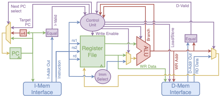
Single Cycle Processor
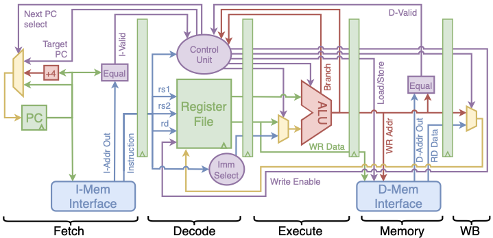
The single cycle processor implements the RV32I instruction set with modules designed around the “textbook” fetch, decode, execute, memory, and write-back stages of a processor . This processor serves as the base for other cores; as such, it has been designed to be as simple as possible. The modules in the single cycle processor are reused or wrapped with additional logic to support features such as pipelining and data forwarding. A block diagram of the processor is shown in Figure 5. The single cycle processor has instruction and data memory interfaces compatible with every cache and memory subsystem provided in the platform. Due to the single cycle operation, NOPs are inserted between BRAM or off-chip memory accesses. An asynchronous memory is provided to avoid NOPs, but it cannot be implemented in FPGA BRAM and must be kept small to prevent the memory from using too many device resources.
By using the Verilog hex output from the included compiler toolchain described in Section 21.3, users are able to compile a bare-metal C program and run it on an FPGA implementation of the processor. Synthesis results have been collected and are shown in Table [synthesis_results]. Note that the Logic Element usage is high because the memory is implemented in Look Up Tables (LUT), because of the asynchronous memory system used.
 />
/>
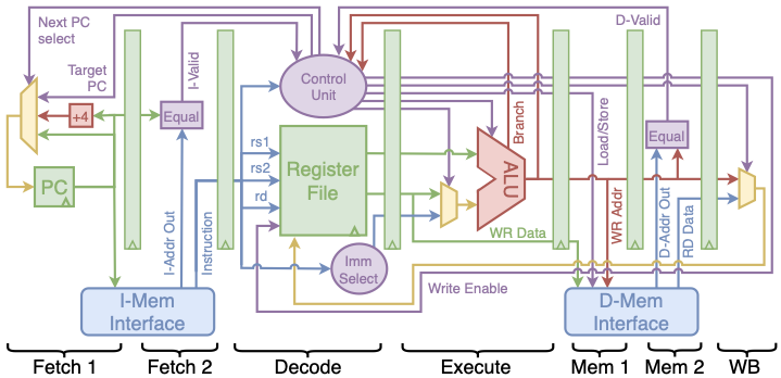
Five Stage Pipeline
The five stage processor is implemented by using the base modules from the single cycle processor as a starting point and adding pipeline registers between the combinational fetch, decode, execute, memory and writeback modules. The single cycle control logic module is wrapped with additional logic to support the stall and bypass signals needed for pipelining. Introducing multiple instructions in flight demonstrates how hazard resolution must consider bypassing, stalling, and pipeline flushing.
Pipelining allows for a higher clock frequency; however, NOPs are still inserted between synchronous memory operations because there is no pipeline register between the address input and data output of the memory interfaces. Asynchronous memories must still be used to avoid NOPs between instruction fetches. Note, however, that the addition of pipeline stages allows some synthesis tools to implement an asynchronous main memory (without caches) in FPGA BRAM. The five-stage pipelined processor has two variants. The first uses only pipeline stalls and flushes when a pipeline hazard is detected. The second implements data forwarding to avoid stalls for most hazards. Stalling and forwarding logic is wrapped around the base control unit used in the single cycle core. A multiplexer is wrapped around the decode logic to output forwarded data when needed. Wrapping the base modules to build the five stage pipeline maximizes IP reuse and allows for user base module customizations to be carried through their core design space.
/>
Seven Stage Pipeline
The seven-stage pipelined processor builds on the base modules in the single cycle processor and the pipeline related modules introduced with the five stage processor. It adds registers between the address inputs and data outputs of the memory interfaces to avoid inserting NOPs while waiting for synchronous memory operations. With these extra pipeline stages, BRAM reads and cache hits no longer need to insert NOPs. The additional pipeline stages can be seen in the seven stage pipeline block diagram shown in Figure 7.
Placing extra stages between the memory interface input and outputs enables logic to check that a memory read is valid while the next operation is issued. Operations in cacheless implementations with on-chip BRAM will always be valid; however, the addition of caches means that cache misses could delay valid read data. In the event of a cache miss, the received data is marked invalid by the memory and the processor stalls until the requested memory has been retrieved. On cache hits, execution continues normally with no inserted NOPs. The extra registers in the seven stage pipeline yield an improved maximum clock frequency. The extra pipeline registers lead to simplified control logic, resulting in a slightly reduced area. Synthesis results for the seven stage pipeline are shown in Table [synthesis_results].
 />
/>
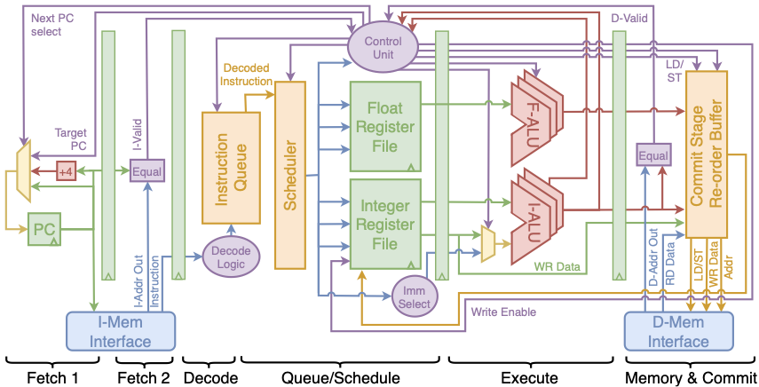
Out of Order Processor
The Out-Of-Order (OOO) core enables exploration of advanced architectural features including a superscalar architecture, instruction scheduling, and complex hazard resolution. The OOO processor supports out-of-order execution with in order commit. The number of ALUs has been parameterized to allow users to explore the impact of a varying number of functional units on processor performance.
The OOO processor implements the RV32F instruction set extension to create more opportunities for out-of-order execution. In order to support the floating point extension, a floating point register file and floating-point execution units were added to the processor. The base decode and control units have been expanded with extra logic to support the new floating point instructions.
The OOO core adds three multi-cycle modules to the processor pipeline: (1) an instruction queue, (2) a scheduler, and (3) a commit stage. These three stages do not reuse any of the base modules from the in-order cores discussed previously. Figure 8 shows a block diagram of the OOO micro-architecture.
In the out-of-order processor, instructions are fetched and decoded before being placed in the new instruction queue stage. The instruction queue length can be modified by the user to trade off performance and area. The queue is implemented as a priority queue, in which the highest priority (longest waiting) instruction without any hazards is scheduled next.
The scheduler module supports a parameterized number of floating point and integer ALUs. When both an instruction and an ALU are ready, the scheduler assigns the instruction to the available ALU. After the instruction has completed its execution with respect to the ALU, it continues through the pipeline into the commit stage. Up to one instruction is scheduled each clock cycle. ALUs can be pipelined to ensure their utilization remains high, offering yet another design space exploration trade off.
Memory operations wait in the commit module until the memory access has completed. Instructions in the commit module are buffered and sent to the writeback unit in order. Instructions are re-ordered based on the priorities used in the instruction queue. An instruction’s ‘rd’ value is stored in a table in the instruction queue stage. Hazards are detected by comparing the ‘rd’ values of in-flight instructions to the ‘rs1’ and ‘rs2’ values of instructions entering the queue. An instruction’s ‘rd’ value is cleared from the table in the instruction queue stage after the instruction exits the writeback stage, completing its execution.
 />
/>
Platform Evaluation
Stress Testing Example of the Platform
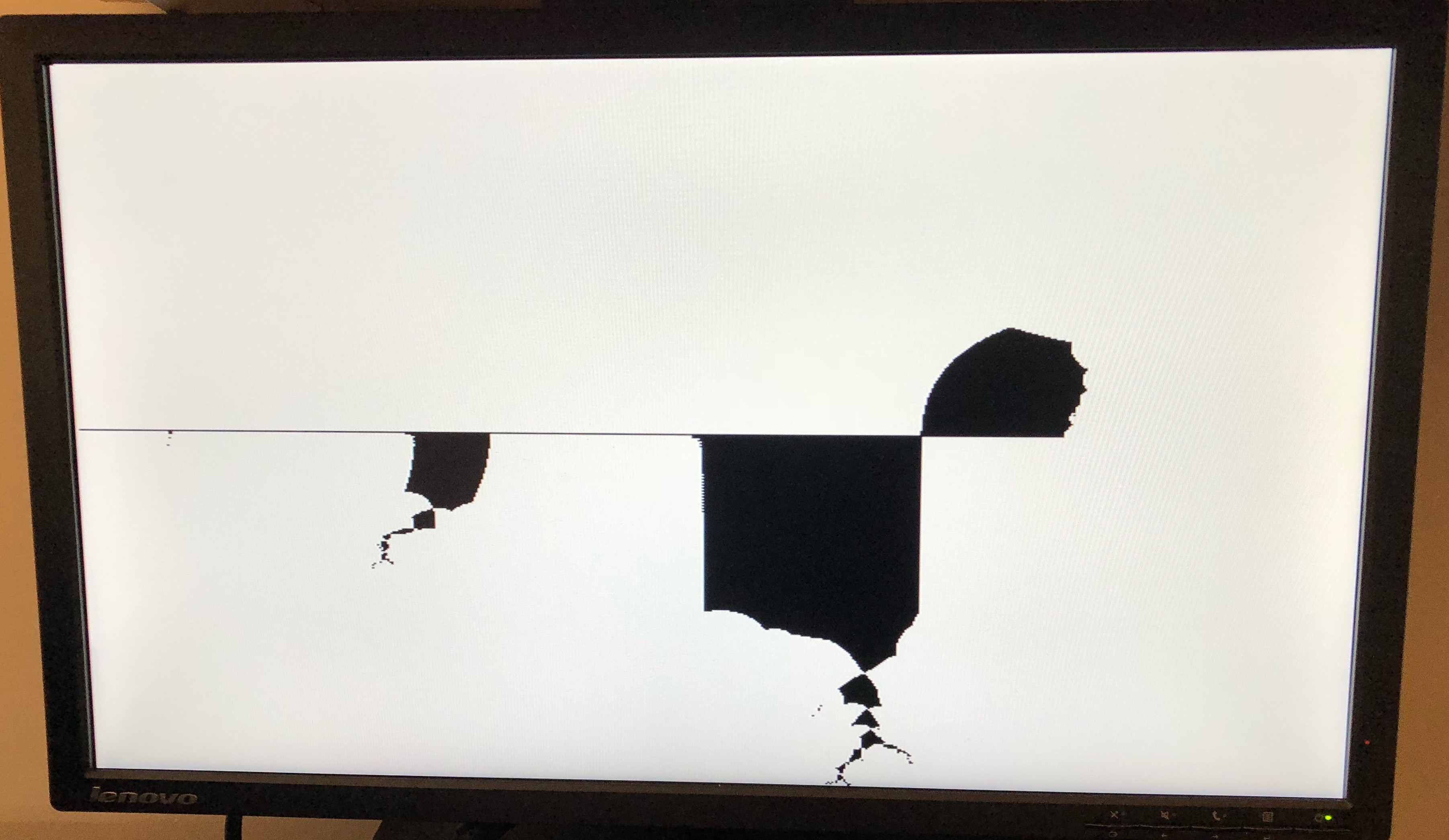
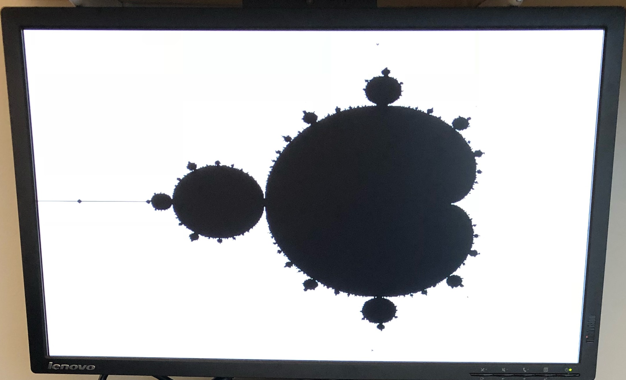
The different versions of the processing cores in this platform lay the groundwork for a quick micro-architecture design exploration. The cores included in this platform provide various levels of complexity for users to build on. In order to evaluate the ease of use of the platform, we instantiate a simple faulty core and add peripheral devices such as a memory mapped VGA frame buffer. The frame buffer is used to render a Mandelbrot fractal. Testing the rendering program revealed that the fault was injected in the ALU module and caused it to execute signed operations incorrectly. Figure 9 compares the incorrect rendering with the correct rendering. Finding and fixing this bug is an example of how this design space exploration platform enables users to make additions easily and expand core designs.
Design Space Exploration
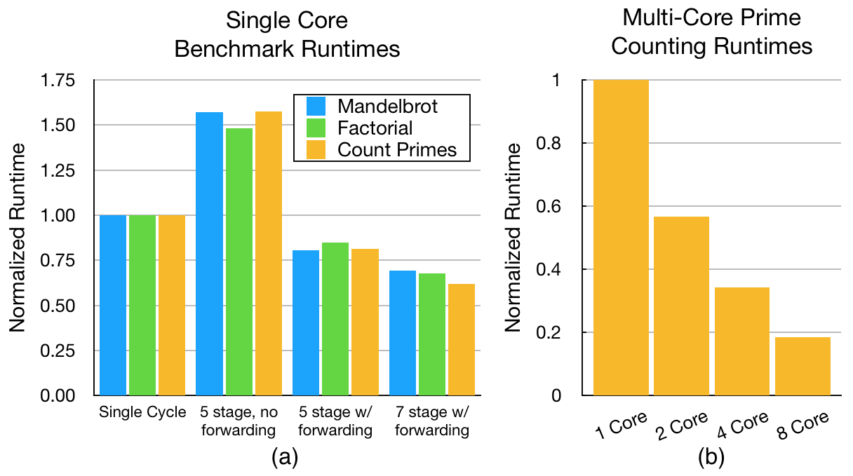
To evaluate the performance of the platform and showcase the extent of design space exploration possible, we benchmark several processing system configurations. First, we compare single cycle, five-stage pipeline (with and without data forwarding) and seven-stage pipeline (with data forwarding) cores with asynchronous memory in the single cycle system and synchronous memory in the pipelined systems. Each system uses a dedicated instruction and data memory module in a single core configuration. These configurations do not use caches to avoid paying the penalty of cache misses without the benefit of larger off-chip main memory. Second, we compare multi-core systems connected via a bus between the level 1 and level 2 caches. In each multi-core system, the seven-stage pipelined core is used.
To compare the single-core, cacheless processor configurations, three different benchmark programs are run on each core. One benchmark computes the factorial of an integer. The second benchmark counts the number of prime numbers between two numbers. A third benchmark computes the Mandelbrot set at a given resolution and checksums the result.
Each benchmark is executed in an RTL simulation of the configured processing system. The number of cycles needed to complete the program execution is recorded. The estimated $`F_{\max}`$ (obtained from synthesis tools) of each core and the number of clock cycles in each program execution is used to compute the runtime of the benchmark. Table [runtime_table] reports the number of cycles for each benchmark. Figure 10 compares the runtime of each benchmark on each of the configured systems. The runtimes are normalized to the single cycle core’s runtime.
The single cycle system executes each benchmark in the fewest cycles but the low clock frequency hurts the program runtime. The single cycle core’s clock frequency is roughly half that of the other cores because the asynchronous main memory is implemented in logic elements instead of the faster BRAMs.
| P1.45cm p0.9cm p1.0cm l l | Core & Clock & Prime & Factorial &
Mandelbrot
Type & Freq. & Cycles & Cycles & Cycles
Single Cycle & 29.0 MHz & 3,464k & 59k & 488k
Stage Stalled & 62.6 MHz & 11,789k & 190k & 1,654k
Stage Bypassed & 61.5 MHz & 5,891k & 107k & 833k
Stage Bypassed & 81.1 MHz & 6,833k & 113k & 948k
| P2cm P3cm P2.1cm | Core & Clock & Number of
Count & Frequency& Cycles
& 61.7 MHz & 7,995,845
& 59.5 MHz & 4,373,431
& 60.0 MHz & 2,671,258
& 59.5 MHz & 1,426,346
The five-stage pipelined processor has a much higher clock frequency than the single cycle core, but must stall the pipeline for each hazard encountered. Pipeline stalls lead to a much higher number of cycles needed to execute the program. The five-stage pipeline without data forwarding has the highest program runtime of the tested cores. Adding data forwarding to the five-stage pipeline cuts the program runtime in half, yielding runtimes better than the single cycle core.
The seven-stage pipeline adds two stages to the five-stage pipeline to support synchronous memories without inserting NOPs. These extra stages increase the clock frequency but also increase the number of cycles needed to compute the target address of branch and jump instructions. The five-stage pipeline must wait two cycles before a jump or branch address is ready while the seven-stage pipeline must wait three cycles. Neither pipeline has a branch predictor. The extra cycles spent stalling are canceled out by the higher clock frequency of the seven-stage pipeline. The seven-stage pipeline has the best runtime for each benchmark.
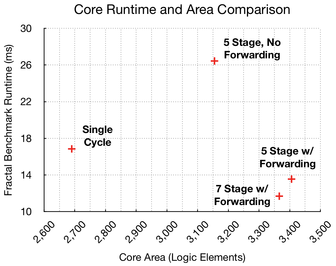
Comparing the five-stage pipeline with and without data forwarding demonstrates the effectiveness of forwarding in resolving pipeline hazards. Comparing the five- and seven-stage pipelines with data forwarding illustrates how the number of bubbles inserted in the pipeline during jumps, branches, and the remaining load-use hazards impacts program runtime. Figure 11 plots the Mandelbrot fractal benchmark runtime versus the core area to visualize the area and performance trade-off. Only the area of the core is considered; area used by memory is ignored here. The area usage of each core is discussed in Section 17.3.
To compare multi-core architectures using caches, the same prime counting benchmark used in the single core tests is parallelized and run on multi-core systems with different core counts. The L1 instruction and data caches in the configured multi-core systems have four 32-bit words per cache line and are 4-way set associative. There are 256 lines in each L1 cache. The shared L2 cache in each processor also has four 32-bit words per cache line and is 4-way set associative. The L2 cache has 512 cache lines. As expected, increasing the number of cores decreases the program runtime. Table [multicore_runtime_table] shows the clock frequency of each multi-core processor and the number of cycles needed to execute the benchmark program. Figure 10 compares the runtime of each processor. Note that each time the number of cores is doubled, the runtime is nearly halved.
By providing different core options with a range of pipeline depths and clock frequencies, the platform simplifies analysis of performance and area tradeoffs. The analysis presented here was limited to core micro-architecture, cache design and number of cores but many more options are available for fine tuning.
Synthesis Results
The runtime lengths presented in Tables [runtime_table] and [multicore_runtime_table] are based on simulations, but each core is fully synthesizable. All synthesis results presented here target an Altera Cyclone IV FPGA with 150k logic elements.
Table [synthesis_results] shows the “ADDRESS_BITS” parameter value, logic element usage, BRAM usage and worst case $`F_{\max}`$ for each cacheless core type. In Table [synthesis_results], the “ADDRESS_BITS” parameter was set to 12 for each pipelined core. Twelve address bits yields 4k 32-bit word addresses for each instruction and data memory (8k words total). The single cycle core uses the asynchronous memory and must implement its memory in logic elements. To ensure the single cycle design fits on the device, it was synthesized with just 1k word memories.
The cores in Table [synthesis_results] do not use caches. Separate instruction and data RAMs are connected directly to the processors memory interfaces to act as main memory. Using simple memory minimizes the memory system’s impact on resource usage. These results focus on the cores themselves. Tables 4, 5 and 6 show cache resource usage in isolation. Table [multicore_synthesis_results] shows synthesis results for several multi-core processor configurations.
Table 4 shows synthesis results for varying L1 cache sizes targeting the same Cyclone IV FPGA mentioned above. The number of logic elements and BRAM used as well as the maximum clock frequency are reported. Each cache is 4-way set associative and has 4 word (16 Byte) cache lines. The synthesis results show that varying the cache size while maintaining the same line size and associativity only marginally changes the logic element usage and $`F_{\max}`$. Only the BRAM usage is significantly impacted by cache size.
Table 5 shows synthesis results for 4kB L1 caches with 4 word (16 Byte), cache lines and various associativities. Intuitively, the number of logic elements grows with the associativity while $`F_{\max}`$ shrinks. The BRAM usage grows slowly with the associativity. The 16-way associative cache uses 2k more BRAM bits than the 1-way (direct mapped) cache. The increase in BRAM usage with higher associativities can be explained by the higher BRAM usage in the ‘replacement_controller’ module, which implements the true least recently used (LRU) replacement policy.
Table 6 shows synthesis results for 4kB L1 caches with line widths ranging from 1 word (4 Bytes) to 16 words (64 Bytes). Varying the line width trades off BRAM and logic elements. Smaller line widths use more BRAM bits for tag storage, while larger line widths use more logic elements to implement registers and buses to handle wider cache lines.
Table [multicore_synthesis_results] shows the resource usage for processors with 1, 2, 4 and 8 cores. The cores used in the multi-core processor are versions of the 7-stage pipelined core. The L1 caches, shared L2 cache, and coherence controller modules add a significant area overhead but enable the use of complex memory hierarchies. The significantly larger BRAM usage in the multi-core processors stems from the large cache and on-chip main memory. The memory in the single core processors was made to be smaller because larger memories were not needed for the benchmarks. Note that the BRAM usage for the 8-core processor is slightly greater than what is available on the device. We have included the results here because moving the main memory to off-chip SRAM available on our development board would allow the caches to fit within the device BRAM without significantly impacting the performance.
The memory hierarchy for each of the processors in Table [multicore_synthesis_results] uses the same parameters. 16kB L1 caches, 32kB L2 caches and a main memory of 256kB.
The different cores and cache configurations supported by the platform enable users to examine the difference between design choices quickly. Additional configuration options, including NoC routing, NoC topology, and on/off-chip main memory configurations have not been included here due to space restrictions.
Each core builds off of the same set of base modules, making it easy to integrate experimental features into several of them by modifying only the base module. This extensibility opens up even more possibilities for design space exploration. We have used this technique to add data forwarding, originally added to the five-stage pipeline, to the out-of-order and seven-stage pipeline cores.
|P1.5cm p0.6cm p1.7cm p1.50cm p1.10cm| Core & Addr & Logic & BRAM &
Fmax
Type & Bits & Elements & Bits &
Single Cycle & 10 & 53,448 & 0 & 29.0 MHz
Stage Stalled & 12 & 3,160 & 262,144 & 62.6 MHz
Stage Bypassed & 12 & 3,406 & 262,144 & 61.5 MHz
Stage Bypassed & 12 & 3,366 & 262,144 & 81.1 MHz
|P1.4cm p1.6cm p2.35cm p1.5cm| Core & Logic & Total Memory & Fmax
Count & Elements & Bits (BRAM) & Fmax
& 12,206 & 2,736,128 & 61.7 MHz
& 21,123 & 3,055,616 & 59.5 MHz
& 38,921 & 3,694,592 & 60.0 MHz
& 83,020 & 4,972,544 & 59.5 MHz
| Cache | Addr | Logic | Total Memory | Fmax |
| Size | Bits | Elements | Bits (BRAM) | |
| 1kB | 4 | 3,208 | 10,240 | 79.1 MHz |
| 2kB | 5 | 3,196 | 20,352 | 81.0 MHz |
| 4kB | 6 | 3,198 | 40,448 | 82.6 MHz |
| 8kB | 7 | 3,189 | 80,384 | 81.1 MHz |
| 16kB | 8 | 3,189 | 159,744 | 82.8 MHz |
Synthesis results for various sizes of 4-way set associative L1 caches. Each cacheline is 16 Bytes (four 32-bit words)
| Cache | Addr | Logic | Total Memory | Fmax |
| Ways | Bits | Elements | Bits (BRAM) | |
| 1 | 8 | 2,387 | 39,424 | 104 MHz |
| 2 | 7 | 2,736 | 39,936 | 97 MHz |
| 4 | 6 | 3,198 | 40,448 | 82 MHz |
| 8 | 5 | 4,534 | 40,960 | 66 MHz |
| 16 | 4 | 6,546 | 41,472 | 49 MHz |
Synthesis results for various associativities in 4kB L1 caches. Each cacheline is 16 Bytes (four 32-bit words)
| Line | Addr | Logic | Total Memory | Fmax |
| width | Bits | Elements | Bits (BRAM) | |
| 4 Bytes | 8 | 1,663 | 63,488 | 82 MHz |
| 8 Bytes | 7 | 2,227 | 48,128 | 81 MHz |
| 16 Bytes | 6 | 3,198 | 40,448 | 82 MHz |
| 32 Bytes | 5 | 5,039 | 36,608 | 81 MHz |
| 64 Bytes | 4 | 8,888 | 34,688 | 76 MHz |
Synthesis results for various line widths in 4kB, 4-way set associative L1 caches.
Conclusion
This platform works to address the challenge of fast multi-core design space exploration. By offering highly parameterized cores, cache, memory, and NoC subsystems, our platform allows users to quickly explore a RISC-V architectural design space without the need to develop complex multi-core systems from scratch. A supporting hardware configuration application GUI enables rapid selection of system parameters and RTL generation. Once Verilog is generated by the configuration application, users can investigate how each design decision will impact system properties such as performance, area or timing. Users can add custom features or other modifications to further expand the explorable design space.
Including the necessary compiler tool-chain makes running experiments on
customized hardware systems simpler. The whole platform system is open
source, including all of the RTL code,
toolchain customizations and supporting applications, enabling
users to customize components to fit their needs.
Future Work
The goal of this work is to explore techniques to develop a fast, flexible, multi-core design space exploration platform, enabling users to understand the impact of their design decisions and quickly test different configurations. To expand the number of configuration options available to users further, the authors plan to add several new features to the available cores, including branch predictors, hardware multi-threading, and other RISC-V ISA extensions, such as the floating point (RV32F) or multiply (RV32M) extensions. Each of these new features will be made available as an option for a user’s desired core and incorporated into the hardware configuration GUI.
The platform has already supported, and will continue to support, research relating to secure architectures focused on enabling efficient obfuscation with hardware-software co-design. The improvements described above will be necessary to support additional research focused on developing RISC-V architectures for HPC workloads with efficient distributed memory.
As a design space exploration platform, the explorable design space is only limited by the man-power available to develop configurable features. For this reason, we have released the source code for the entire platform (the RTL, toolchain customizations and GUI application code) in the hope that others in the community can benefit from, and add to the design space exploration capabilities of the tool.
| Cache | Addr | Logic | Total Memory | Fmax |
| Size | Bits | Elements | Bits (BRAM) | |
| 1kB | 4 | 3,208 | 10,240 | 79.1 MHz |
| 2kB | 5 | 3,196 | 20,352 | 81.0 MHz |
| 4kB | 6 | 3,198 | 40,448 | 82.6 MHz |
| 8kB | 7 | 3,189 | 80,384 | 81.1 MHz |
| 16kB | 8 | 3,189 | 159,744 | 82.8 MHz |
Synthesis results for various sizes of 4-way set associative L1 caches. Each cacheline is 16 Bytes (four 32-bit words)
| Cache | Addr | Logic | Total Memory | Fmax |
| Ways | Bits | Elements | Bits (BRAM) | |
| 1 | 8 | 2,387 | 39,424 | 104 MHz |
| 2 | 7 | 2,736 | 39,936 | 97 MHz |
| 4 | 6 | 3,198 | 40,448 | 82 MHz |
| 8 | 5 | 4,534 | 40,960 | 66 MHz |
| 16 | 4 | 6,546 | 41,472 | 49 MHz |
Synthesis results for various associativities in 4kB L1 caches. Each cacheline is 16 Bytes (four 32-bit words)
| Line | Addr | Logic | Total Memory | Fmax |
| width | Bits | Elements | Bits (BRAM) | |
| 4 Bytes | 8 | 1,663 | 63,488 | 82 MHz |
| 8 Bytes | 7 | 2,227 | 48,128 | 81 MHz |
| 16 Bytes | 6 | 3,198 | 40,448 | 82 MHz |
| 32 Bytes | 5 | 5,039 | 36,608 | 81 MHz |
| 64 Bytes | 4 | 8,888 | 34,688 | 76 MHz |
Synthesis results for various line widths in 4kB, 4-way set associative L1 caches.
📊 논문 시각자료 (Figures)