Hardware Implementation of Neural Self-Interference Cancellation
In-band full-duplex systems can transmit and receive information simultaneously on the same frequency band. However, due to the strong self-interference caused by the transmitter to its own receiver, the use of non-linear digital self-interference ca…
Authors: Yann Kurzo, Andreas Toftegaard Kristensen, Andreas Burg
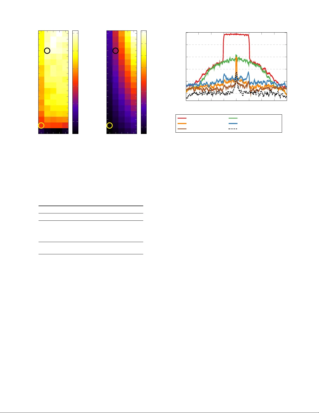
1 Hardware Implementation of Neural Self-Interference Cancellation Y ann Kurzo, Andreas T oftegaard Kristensen, Andreas Bur g, Member , IEEE, Alexios Balatsoukas-Stimming, Member , IEEE Abstract —In-band full-duplex systems can transmit and r e- ceive information simultaneously and on the same frequency band. Howev er , due to the strong self-interfer ence caused by the transmitter to its own receiv er , the use of non-linear digital self- interference cancellation is essential. In this work, we describe a hard ware ar chitecture for a neural network-based non-linear self-interference (SI) canceller and we compare it with our own hardwar e implementation of a conv entional polynomial based SI canceller . Our results show that, for the same SI cancellation performance, the neural network canceller has an 8 . 1 × smaller area and requir es 7 . 7 × less power than the polynomial canceller . Moreo ver , the neural network canceller can achiev e 7 dB more SI cancellation while still being 1 . 2 × smaller than the polynomial canceller and only requiring 1 . 3 × more power . These results show that NN-based methods applied to communications are not only useful from a performance perspective, but can also lead to order -of-magnitude implementation complexity reductions. I . I N T R O D U C T I O N In-band full-duplex (FD) communications have for long been considered to be impractical due to the strong self- interference (SI) caused by the transmitter to its o wn receiver . Howe v er , recent work on the topic (e.g., [2], [3], [4]) has demonstrated that it is, in fact, possible to achiev e sufficient SI cancellation (SIC) to make FD systems viable. T ypically , SIC is performed in both the radio frequency (RF) domain and the digital domain to cancel the SI signal down to the lev el of the receiv er noise floor . There are sev eral RF cancellation methods, that can be broadly categorized into passive RF cancellation and active RF cancellation . Some form of RF cancellation is generally necessary to av oid saturating the analog front-end of the receiv er . Passiv e RF cancellation can be obtained by using, e.g., circulators, directional anten- nas, beamforming, polarization, or shielding [5]. Activ e RF cancellation is commonly implemented by transforming the transmitted RF signal appropriately to emulate the SI channel using analog components and subtracting the resulting SIC signal from the received SI signal [2], [4]. Alternatively , an Y . Kurzo is with ON Semiconductor, 2074 Marin-Epagnier , Switzerland (e-mail: yann.kurzo@gmail.com). A. Kristensen and A. Burg are with the T elecommunications Circuits Labo- ratory , ´ Ecole polytechnique f ´ ed ´ erale de Lausanne, 1015 Lausanne, Switzerland (e-mail: { andreas.kristensen,andreas.burg } @epfl.ch). A. Balatsoukas-Stimming is with the Eindhoven Uni versity of T echnology , 5600 MB Eindhoven, The Netherlands (e-mail: a.k.balatsoukas.stimming@tue.nl). Parts of this work were presented at the 2018 Asilomar Conference on Signals, Systems, and Computers [1]. This work was supported by the Swiss National Science Foundation under project #200021 182621. additional transmitter can be used to generate the SIC signal from the transmitted baseband samples [3]. Howe v er , a residual SI signal is typically still present at the receiv er after RF cancellation has been performed. This resid- ual SI signal can, in principle, be easily canceled in the digital domain, since it is caused by a known transmitted signal. Unfortunately , in practice, sev eral transcei ver non-linearities distort the SI signal. Some examples of non-linearities in- clude baseband non-linearities (e.g., digital-to-analog con- verter (DA C) and analog-to-digital conv erter (ADC)) [6], IQ imbalance [6], [7], phase-noise [8], [9], and power amplifier (P A) non-linearities [6], [7], [10], [11]. These ef fects need to be taken into account using intricate polynomial models to cancel the SI to the level of the receiv er noise floor . These polynomial models perform well in practice, but their implementation complexity grows rapidly with the maximum considered non-linearity order . Principal component analysis (PCA) is an effecti ve complexity reduction technique that can identify the most significant non-linearity terms in a parallel Hammerstein model [11]. Howe ver , with PCA-based methods, the transmitted digital baseband samples need to be multiplied with a transformation matrix to generate the SIC signal, thus introducing additional complexity . Moreover , whenever the SI channel changes, the high-complexity PCA operation needs to be re-run. T o the best of our kno wledge, no hardware implementation of a polynomial SI canceller has been reported in the open literature to date. Only the work of [12] has made a step in this direction, since the authors considered quantization aspects of polynomial SI cancellers. In the past few years, there has been renewed interest in the use of neural networks (NNs) to augment or replace a range of signal processing tasks in communications systems [13], [14], [15], [16], [17], [18]. NNs are particularly well-suited to tackle non-linear signal processing problems, where traditional model-based algorithms are unav ailable or too complex for analytical treatment. Howe ver , NN-based solutions can also be used in cases where traditional model-based algorithms suffer from prohibiti vely high implementation complexity . For example, NNs hav e been used to successfully perform digital predistortion (DPD) in wireless systems [19], [20], non-linear leakage cancellation in FDD transceiv ers [21], as well as opti- cal fiber non-linearity compensation [22]. NNs have also been used for non-linear SIC in full-duplex communications [23], [24], [25] and it was shown in [23] that they can achiev e similar SIC performance with a state-of-the-art polynomial SIC model, but with much lower complexity . The communications subsystems of embedded devices are 2 Digital Cancellation D A C P A BP Filter x IQ Mixer x DA C x IQ x P A RF Cancellation BP Filter LN A ADC h SI y RX y LNA y IQ y IQ Mixer Local Oscillator Fig. 1. Block diagram of a full-duplex transceiv er with active RF SIC and digital SIC. A few components have been omitted for simplicity , a more detailed diagram can be found in [11]. typically implemented using dedicated hardware instead of general-purpose processors. The main reason for this is that using dedicated hardware enables very high energy efficienc y , which is particularly desirable in mobile platforms. As such, dedicated hardware solutions for NN-assisted communications systems are essential. Existing NN hardware accelerators, such as [26], [27], mainly target applications where both the size of the NN and the number of inputs is very large, and where producing a few tens of outputs per second is sufficient. Communications applications, on the other hand, use relatively small NNs with few inputs, b ut need to provide millions of outputs per second. As such, communications applications generally require more highly parallelized NN hardware accelerator architectures. Howe ver , to date, only a small number of works ha ve considered these hardware- related issues in the context of communications applications. Specifically , the works of [28], [29] study NN quantization as a first step towards hardware implementation, while the authors of [1], [30] describe actual hardware implementations of simple NNs for SIC in full-duplex communications and DPD, respectively . Contribution: In this work, we present a hardware imple- mentation of the SIC method proposed in [23] to quantify and translate the computational complexity gains ov er the state-of-the-art polynomial based model of [11] into real- world hardware resource utilization gains. Contrary to [1], [23], we use a more realistic and well-defined measurement setup that results in a completely ne w and more challenging dataset with more non-linear content. Since, to the best of our knowledge, no polynomial SI canceller implementations hav e been reported in the literature, we also present a hardware architecture for a reference polynomial SI canceller . W e note that this hardware architecture can also be used for other related applications such as digital predistortion and leakage cancellation in FDD transcei vers. W e provide FPGA and ASIC implementation results that clearly demonstrate the significant gains with respect to the polynomial SI canceller that can be achiev ed by an NN-based SI canceller in terms of resource utilization, throughput, and energy ef ficiency . Outline: The remainder of this paper is organized as fol- lows. Section II provides background on full-duplex commu- nications and digital SIC using polynomial cancellers, while Section III describes how SIC can be achieved using NNs. In Section IV, we describe our proposed NN-based SI canceller hardware architecture and, in Section V, we describe our proposed baseline polynomial-based SI canceller hardware architecture. In Section VI, we compare the performance and the complexity of a con ventional polynomial SI canceller with the NN-based SI cancellers. In Section VII, we also provide FPGA and ASIC implementation results. Finally , Section VIII concludes this paper . I I . C O N V E N T I O N A L D I G I TA L S E L F - I N T E R F E R E N C E C A N C E L L A T I O N Fig. 1 shows a block diagram of a full-duplex transceiver . On the transmitter side, the digital baseband samples x [ n ] ∈ C , where n is the sample index, are con verted to an analog signal using a DA C, up-con verted to a carrier frequency f c using an IQ mixer , amplified using a power amplifier (P A), and filtered using a bandpass (BP) filter . The transmitted signal leaks to the receiv er through an SI channel h SI and is then filtered using a BP filter, amplified using an LN A, downcon verted using an IQ mixer , and digitized using an ADC. The SI channel, h SI , also models the passiv e RF SIC. An RF cancellation signal is subtracted from the recei ved SI signal at some point before the LNA to av oid saturating the receiv er . Since the transmitter and the receiv er are co-located, they share a common local oscillator (LO) signal to minimize the ef fect of phase noise on the SI signal [9]. If we assume, for simplicity of exposition, that there is no signal-of-interest from a remote node and no thermal noise, then the receiv ed signal y [ n ] in Fig. 1 consists only of the residual SI signal after RF SIC has been performed. W e denote the receiv ed signal in this special case by y SI [ n ] . The goal of digital SIC is to reproduce an accurate copy of y SI [ n ] , denoted by ˆ y SI [ n ] , based on samples of the transmitted baseband signal x [ n ] . This signal is then subtracted from y [ n ] so that the residual SI signal is y SI [ n ] − ˆ y SI [ n ] . If ˆ y SI [ n ] is reconstructed perfectly , then the SI can be canceled entirely and y SI [ n ] − ˆ y SI [ n ] = 0 . In practice, as discussed previously , due to the presence of thermal noise and transcei ver 3 non-linearities, perfect SIC is difficult to achiev e. The SIC performance C dB is typically ev aluated as: C dB = 10 log 10 P n | y SI [ n ] | 2 P n | y SI [ n ] − ˆ y SI [ n ] | 2 . (1) A. Linear Self-Interference Cancellation Linear SIC is the simplest form of SIC that ignores all non- linear effects of the various components in Fig. 1. The linear SIC signal is constructed as [4]: ˆ y SI [ n ] = L − 1 X l =0 ˆ h [ l ] x [ n − l ] , (2) where ˆ h [ l ] ∈ C , l ∈ { 0 , . . . , L − 1 } , models the SI channel, h SI , and any other memory ef fect in the transceiver chain. The parameters ˆ h [ l ] can be obtained from training samples either in a one-shot fashion using standard least-squares (LS) estimation or adaptively using an iterativ e version of the LS estimation algorithm, such as least mean squares (LMS) or recursiv e least squares (RLS). B. P olynomial Non-Linear Self-Interfer ence Cancellation Each activ e component in the transceiv er model shown in Fig. 1 is generally a dynamic non-linear system. This means that linear cancellation alone is, in most cases, not accurate enough to cancel a sufficiently large fraction of the SI signal. It has been shown that the transmitter IQ imbalance and the P A non-linearities typically dominate all remaining non-linearities [10], [11]. This is true in particular when the transmitter and receiver chains use the same local oscillator signal for upcon version, as shown in Fig. 1, so that the effect of phase noise becomes negligible [9]. As such, the SIC signal ˆ y SI [ n ] can be constructed as [10], [11]: ˆ y SI [ n ] = P X p =1 , p odd p X q =0 L − 1 X l =0 ˆ h p,q [ l ] x [ n − l ] q x ∗ [ n − l ] p − q , (3) where ˆ h p,q [ l ] ∈ C and only odd values for p are considered because e ven harmonics typically lie out-of-band and are filtered out by the transmitter and receiver BP filters. The model in (3) is linear with respect to the parameters ˆ h p,q [ l ] , and therefore, similarly to linear SI estimation, the parameters ˆ h p,q [ l ] can be estimated based on training samples using some variant of the LS estimation algorithm. The basis functions of the polynomial model in (3) are defined as: BF p,q ( x ) = x q ( x ∗ ) p − q . (4) The number of distinct basis functions in (3) is [11]: N BF = L 4 ( P + 1) ( P + 3) . (5) Using (4), the expression for ˆ y [ n ] in (3) can be re-written in a more compact form: ˆ y SI [ n ] = P X p =1 , p odd p X q =0 L − 1 X l =0 ˆ h p,q [ l ] BF p,q ( x [ n − l ]) . (6) W e note that linear cancellation is a special case of the polynomial model in (6) when only considering the single term for p = 1 and q = 1 . C. Computational Complexity A multiplication between two complex numbers x 1 = a + j b and x 2 = c + j d can be performed in a straightforward manner as x 1 x 2 = ( ac − bd ) + j ( ad + bc ) . This requires two real-valued additions and four real-valued multiplications. Howe ver , it is also possible to first compute s 1 = ac , s 2 = bd , and s 3 = ( a + b )( c + d ) so that x 1 x 2 = ( s 1 − s 2 ) + j ( s 3 − s 1 − s 2 ) . This requires five real-valued additions and three real-valued multiplications. Since hardware multipliers are typically sig- nificantly more complex than hardware adders, we assume the latter method is used to minimize the number of multipliers. Thus, it can directly be deduced from (2) that the total number of real-valued multiplications and additions that are required by the linear SI canceller is: N ADD,lin = 7 L − 2 , (7) N MUL,lin = 3 L. (8) Moreov er , if we ignore the computation of the basis functions for simplicity , 1 the total number of real-valued multiplications and additions that are required by the polynomial SI canceller (which also includes the linear cancellation term) is [23]: N ADD,poly = 7 4 L ( P + 1) ( P + 3) − 2 , (9) N MUL,poly = 3 4 L ( P + 1) ( P + 3) . (10) W e note that the expression for N ADD,poly in our previous work of [23] erroneously ignored the fi ve real-valued additions that are required to implement each complex multiplication. As such, the actual complexity of the polynomial canceller is even higher than that reported in [23]. I I I . N E U R A L N E T W O R K N O N - L I N E A R D I G I TA L S E L F - I N T E R F E R E N C E C A N C E L L A T I O N Polynomial SIC models such as (6) work well in practice but are often highly redundant in the sense that many of the ˆ h p,q [ l ] parameters are very close to zero. NN-based SI cancellers, on the other hand, can extract the essence of the non-linear structure of the SI signal from training data, which often significantly reduces the complexity of the SIC model [23]. A challenge when using NN cancellers is that the NN training process is inherently noisy due to the use of mini-batches for gradient estimation, which makes it dif ficult to achiev e a very accurate reconstruction of the SI signal [25]. T o overcome this problem, [23] used a NN to reconstruct only a particular part of the SI signal, while using conv entional linear cancellation for the remainder of the SI. Specifically , in [23] the SI signal was conceptually decomposed into a linear component and a non-linear component: y SI [ n ] = y SI,linear [ n ] + y SI,nl [ n ] . (11) 1 W e note that this simplification is justified in Section V. 4 <{ x [ n ] } ={ x [ n ] } <{ x [ n − 1] } ={ x [ n − 1] } . . . . . . <{ x [ n − L + 1] } ={ x [ n − L + 1] } . . . <{ ˆ y SI,non-linear [ n ] } ={ ˆ y SI,non-linear [ n ] } Fig. 2. Example of a neural network with one hidden layer for the reconstruction of the non-linear component y SI,nl [ n ] of the SI signal [23]. The SIC is carried out in two steps. First, linear cancellation is used to reconstruct ˆ y SI,linear [ n ] as: ˆ y SI,linear [ n ] = L − 1 X l =0 ˆ h [ l ] x [ n − l ] . (12) The parameters ˆ h [ l ] are obtained using LS estimation while considering the substantially weaker signal ˆ y SI,nl [ n ] as noise. The linear SIC signal is then subtracted from the SI signal to obtain: y SI,nl [ n ] ≈ y SI [ n ] − ˆ y SI,linear [ n ] . (13) The task of the NN is limited to reconstructing y SI,nl [ n ] based on the appropriate x [ n ] samples. As is common practice when training NNs, we normalize the input and output training samples so that x [ n ] and y SI,nl [ n ] hav e unit variance (i.e., the variance of the real part and the variance of the imaginary part are both equal to 0 . 5 ) and zero mean. T o perform SIC on the test data, the output of the NN is denormalized using the mean and variance estimated based on the training data. A. Neural Network Structure Due to the universal approximation theorem [31], a feed- forward NN with one hidden layer, as depicted in Fig. 2, is sufficient to reconstruct the non-linear SI signal. While the work of [23] only considered feedforward NNs with one hid- den layer, it is possible to use any NN architecture to generate ˆ y SI,nl [ n ] . In particular , [25] employed a deep feedforward NN and showed that using many layers with few neurons per layer can ha ve significant computational comple xity adv antages with respect to a shallow NN SI canceller that uses a single layer with more neurons. In all cases and as sho wn in Fig. 2, the cancellation NNs hav e 2 L input nodes, which correspond to the real and imaginary parts of the L delayed versions of x [ n ] , and two output nodes, which correspond to the real and imaginary parts of the target ˆ y SI,nl [ n ] sample. In the following, we denote the number of hidden layers by N l and the number of hidden nodes per layer N h . Let the vector l 0 contain the 2 L inputs to the NN: l 0 = <{ x [ n ] } ={ x [ n ] } . . . <{ x [ n − L +1] } ={ x [ n − L +1] } T . (14) The outputs of the first hidden layer neurons are given by: l 1 = f 1 ( W 1 l 0 + b 1 ) , (15) where W 1 is an N h × 2 L matrix containing the hidden layer weights, b 1 is an N h × 1 vector containing the hidden layer biases, and f 1 ( · ) is the (vectorized) non-linear activ ation function used in the first hidden layer . The outputs of the neurons in the hidden layers 1 < l ≤ N l are: l l = f l ( W l l l − 1 + b l ) , (16) where W l is an N h × N h matrix containing the hidden layer weights, b l is an N h × 1 vector containing the hidden layer biases, and f l ( · ) is the (vectorized) non-linear activ ation function used in hidden layer l . Finally , the outputs of the output layer neurons are given by: l N l +1 = f N l +1 ( W N l +1 l N l + b N l +1 ) , (17) where W N l +1 is a 2 × N h matrix containing the output layer weights, b N l +1 is a 2 × 1 vector containing the output layer biases, and f N l +1 is the activ ation function used in the output layer . As can be seen in Fig. 2, for l N l +1 we have: l N l +1 = <{ ˆ y nl [ n ] } ={ ˆ y nl [ n ] } T . (18) The goal of the NN is to minimize the mean squared error between the expected NN output and the actual NN output: MSE = 1 N N − 1 X n =0 ( <{ y SI,nl [ n ] } − <{ ˆ y SI,nl [ n ] } ) 2 + 1 N N − 1 X n =0 ( ={ y SI,nl [ n ] } − ={ ˆ y SI,nl [ n ] } ) 2 , (19) where N is the total number of training samples. The MSE in (19) is minimized by choosing appropriate values for W l , b l , l ∈ { 1 , . . . , N l + 1 } , using back-propagation [32]. B. Computational Complexity Let us assume that the NN uses the popular ReLU activ ation function in the hidden layers (which has similar complexity to a real-valued addition (i.e., f l = ReLU ( x ) = max( 0 , x ) , l ∈ { 1 , . . . , N l } ) and a linear activ ation function in the output layer (i.e., f N l +1 ( x ) = x ). Then, the number of real- valued multiplications and additions that are required by a NN canceller with a single hidden layer and N h hidden neurons is [23]: N ADD,NN = (2 L + 3) N h + 7 L, (20) N MUL,NN = (2 L + 2) N h + 3 L, (21) where the second term in both e xpressions comes from the linear SI canceller that is required for the NN SI canceller to work. Moreov er , two additions are required to add the output of the linear SI canceller with the output of the NN canceller . 2 For the more general NN described in [25] with N l hidden layers with N h neurons each, (20)-(21) can be generalized to: N ADD,NN = (2 L + 3 + ( N l − 1)( N h +1)) N h + 7 L, (22) N MUL,NN = (2 L + 2 + ( N l − 1) N h ) N h + 3 L. (23) 2 W e note that these two additions were not included in [23], but we include them here for the sake of accuracy . 5 y [ n ] Real and Imaginary x [ n ] x [ n − 1] . . . x [ n − L + 1] Real and Imaginary Linear Appr oximator ˆ h Neural Network w i,j and b j Denormalization + − y c [ n ] Real and Imaginary + ˆ y nn [ n ] ˆ y lin [ n ] ˆ y [ n ] Fig. 3. High-lev el architecture on the NN-based SIC scheme [1]. I V . N E U R A L N E T W O R K C A N C E L L E R H A R D W A R E A R C H I T E C T U R E In this section, we describe a generic hardware architecture that can be used to implement both the shallow NN-based SI canceller of [23] and deeper NN-based SI cancellers such as the ones described in [25]. W e first pro vide an o vervie w of the architecture, which is followed by a more detailed explanation of each component. In Fig. 3, we show the high- lev el architecture of a general NN-based canceller . The set of baseband samples { x [ n ] , . . . , x [ n − L + 1] } is given as an input to a linear SI canceller and a NN-based SI canceller . These two SI cancellers operate in parallel to generate the linear and non-linear cancellation signals, respectively , which are then added (after the denormalization step for the NN) to produce the cancellation signal ˆ y SI [ n ] . A. Macr o-Pipeline Ar chitectur e As sho wn in the example of Fig. 4, in our architecture, the canceller NN layers are mapped to macro-pipeline stages. Each macro-pipeline stage requires sev eral clock cycles to compute its outputs and it can start its computations as soon as valid outputs from the previous macro-pipeline stage become av ailable. Due to the high throughput requirements of the SIC task, we instantiate one macro-pipeline stage for each layer in the NN that is used for cancellation. Let NE l denote the number of neurons in layer l . W e note that NE 0 = 2 L , NE N l +1 = 2 , and NE l = N h for all hidden layers l ∈ { 1 , . . . , NE l } . The goal of a macro-pipeline stage is to compute l l using expressions of the form (15)-(17). Each element j ∈ { 0 , . . . , NE l − 1 } of l l can be computed as: l l [ j ] = f l b l [ j ] + NE l − 1 − 1 X i =0 W l [ i, j ] l l − 1 [ i ] . (24) The architecture of each macro-pipeline stage is shown in more detail in Fig. 5. More specifically , each macro-pipeline stage contains an input interface, an array of N PE processing elements (PEs), a weights-and-biases memory , a control unit, and an output interface. W e note that for simplicity , all weights, biases, and partial sums hav e a common bit-width of Q bits and saturation is used in case of an overflo w . More sophisticated quantization schemes are possible, but they are beyond the scope of this work. The N PE PEs, whose internal structure is shown in Fig. 6, can be used to compute (24) over multiple clock cycles using Hidden Layer Output Layer Data In V alid In Stall Out Data Out V alid Out Stall In Clock Reset Fig. 4. Example of a macro-pipeline architecture with two stages for a neural network with N l = 1 hidden layers [1]. More macro-pipeline stages can be added to the pipeline to implement neural networks of arbitrary depth N l . one of two possible schedules. In the neuron-by-neuron (NBN) schedule, neurons are processed sequentially and each of the N PE PEs computes a part of the sum in (24) for a giv en neuron j . In the input-by-input (IBI) schedule, the inputs of layer l (i.e., l l − 1 ) are processed sequentially and the N PE PEs update the sum in (24) with the term W [ i, j ] l l − 1 [ i ] for N PE distinct neurons in parallel. As an NBN macro-pipeline stage generates neuron output values sequentially , the optimal accelerator structure consists of an NBN macro-pipeline stage always being followed by an IBI macro-pipeline stage, allowing the IBI stage to start performing computations once the output of the first neuron of the preceding NBN stage has been computed. Once all inputs have been processed by the IBI stage, it immediately outputs multiple values to the NBN stage which follo ws it. Having an NBN stage after another NBN stage means that the second NBN stage would have to wait for all outputs of the previous stage to be generated before any processing can take place, and having an IBI stage follo wed by another IBI stage would mean that the second IBI stage cannot start processing before the first IBI stage has processed all its inputs. This structure of NBN and IBI stages, connected in an alternating fashion, masks a significant part of the latency and reduces the number of interconnects between two consecuti ve macro-pipeline stages. Since the exact architecture of each macro-pipeline stage depends on the processing schedule, we describe the details of the corresponding architectures separately in the next two sections. B. Neur on-by-Neur on Macr o-Pipeline Arc hitectur e 1) Input Interface: The input interface consists of N PE multiplex ers, which route each of the NE l − 1 elements of l l − 1 to the correct PE. 2) Pr ocessing Elements: In the NBN schedule, each PE is only associated with a single neuron, and therefore only a single partial sum needs to be stored in each PE. Thus, the PEs are simple multiply-and-accumulate (MAC) units and the memory shown in Fig. 6 is, in fact, a single Q -bit register . 3) Contr ol Unit: The main tasks of the control unit are to distribute the computations to the PEs and to stall the computations when no valid inputs are av ailable or when the following macro-pipeline stage is not ready to accept ne w inputs. The computations are dispatched to the PEs as follows. When N PE ≤ NE l − 1 , all N PE PEs are used to process a single neuron at a time and NE l l NE l − 1 N PE m clock cycles are required to process all neurons. When N PE > NE l − 1 , we constrain N PE so that N PE = k · NE l − 1 , k ∈ N , and hence k neurons are 6 Input Interface PE (internal memory) N PE Output Interface (tree adder, act. function) Control Unit (counters, memory signal generation) W eight and Bias Memory Data In Pipeline Control Input Selection PE Enable Reset Sum Memory Signals W eights Biases External Memory Data Out Fig. 5. Block diagram of the macro-pipeline stage architecture [1]. processed in parallel and l NE l NE l − 1 N PE m clock cycles are required to process all neurons. 4) W eight and Bias Memories: The weight and bias mem- ories for layer l are used to store W l and b l and they can be written externally to re-configure the NN canceller . The weights are org anized in a memory that is N PE Q bits wide so that all PEs can be provided with data in parallel. A single word of the weight memory contains N PE weight values corresponding to k different neurons. The bias memory , on the other hand, has a bit-width of k Q bits. 5) Output Interface: The output interface adds the partial sums from the N PE PEs using an adder tree, it adds the corresponding biases, and it applies the non-linear activ ation function f l for each of the k neurons that are being processed in parallel. A register is added between the PEs and the output interface to reduce the critical path of the architecture. Moreov er , the output interface forwards the outputs of the k neurons that are processed in parallel to the next macro- pipeline stage. 6) Latency: In the remainder of this work, we select N PE carefully so that both NE l − 1 N PE and NE l NE l − 1 N PE are integers. W ith this setting, an NBN macro-pipeline stage requires L l = NE l NE l − 1 N PE + 1 , (25) clock cycles to produce all outputs of NN layer l . Howe ver , one full set of outputs for a NN layer is actually produced ev ery NE l NE l − 1 N PE cycles, so that the throughput of the NBN macro-pipeline stage in samples per clock cycle is T l = N PE NE l NE l − 1 . (26) Moreov er , the first k outputs of an NBN macro-pipeline stage become av ailable after L l, first = NE l − 1 N PE + 1 , (27) clock cycles. Therefore, a potential IBI macro-pipeline stage that follows can already start its computations after the L first clock cycles and that only k ≤ NE l outputs need to be forwarded to the next stage at a time. C. Input-by-Input Macro-Pipeline Ar chitectur e 1) Input & Output Interfaces: The input and output inter- faces of the IBI macro-pipeline stage are similar to that of the NBN macro-pipeline stage. The main difference is that the IBI output interface forwards the outputs of all NE l neurons that are processed in parallel to the next macro-pipeline stage. × + Memory Data In W eight In 0 Partial Sum 1 0 1 0 Memory Interface Data Out Fig. 6. Detailed view of the PE architecture that is used by both the NBN and the IBI macro-pipeline stages [1]. 2) Pr ocessing Elements: In the IBI schedule, each PE can be associated with multiple neurons. Therefore, sev eral partial sums may need to be stored in each PE. Thus, the PEs are MA C units and the memory shown in Fig. 6 has l NE l N PE m Q bits. 3) Contr ol Unit: In the IBI schedule, when N PE ≤ NE l , all N PE PEs are used to update the NE l neurons of layer l sequentially with a new input value l [ i ] and NE l − 1 l NE l N PE m clock cycles are required to process all neurons. When N PE > NE l , we constrain N PE so that N PE = k NE l , k ∈ N , and k inputs are processed in parallel. Hence, l NE l NE l − 1 N PE m clock cycles are required to process all neurons. 4) W eight and Bias Memories: The weight and bias mem- ories are similar to those of the NBN macro-pipeline stage. A single word of the weight memory contains N PE weights corresponding to k dif ferent neurons. The bias memory has a bit-width of NE l Q bits in the IBI macro-pipeline stage. All memories support external writes to re-configure the canceller . 5) Latency: Similarly to the NBN schedule, we choose N PE carefully so that both NE l N PE and NE l NE l − 1 N PE are always integers. Then, the latency and the throughput are L l = NE l NE l − 1 N PE + 1 , (28) clock cycles and T = N PE NE l NE l − 1 , (29) samples per clock cycle, respectively . Moreover , since all NE l outputs of an IBI macro-pipeline stage become av ailable simultaneously , the number of clock cycles until the first output is identical to L l and also giv en by L l, first = NE l NE l − 1 N PE + 1 , (30) clock cycles. D. Overall Neural Network Canceller Arc hitectur e The overall NN architecture consists of N l macro-pipeline stages with pipeline registers added between them. The first hidden layer uses an NBN macro-pipeline stage and the second hidden layer (or the output layer when N l = 1 ) uses an IBI macro-pipeline stage. Further layers use NBN and IBI macro-pipeline stages in an alternating fashion as pre viously discussed. The NE 0 = 2 L inputs l 0 of the first NBN macro- pipeline stage that implements the computations of the first 7 Basis Functions Calculator/ Memory Complex PE (single register) N CPE Output Block (tree adder) Control Unit (counters, memory signal generation) Complex W eight Memory Data In Pipeline Control Basis Function Selection PE Enable Reset Sum Memory Signals W eights Biases External Memory Data Out Fig. 7. Block diagram of the polynomial canceller architecture. hidden layer are assumed to all be av ailable in parallel. The number of PEs instantiated for layer l is denoted by N PE ,l . The computations for the linear canceller are done in parallel with the NN by instantiating a standard complex FIR filter with N PE , linear complex-v alued PEs. The latency of the linear canceller in clock cycles L linear = L N PE , linear . (31) Since the linear canceller is not pipelined, it holds that T linear = 1 L linear . The throughput of the overall NN canceller architecture is: T = min T linear , min l ∈{ 1 ,...,N l +1 } T l . (32) Since it is typically not very costly in terms of resources to ensure that T linear ≥ T l , l ∈ { 1 , . . . , N l +1 } , in practice T is usually limited by min l T l . As opposed to the throughput, the latency of the ov erall NN canceller is more complicated to derive in general. Howe ver , in the special case where the number of PEs for each layer l is chosen such that no stalling happens and N l + 1 is ev en, the latency can be calculated as: L = max L linear , ( N l +1) / 2 X l =1 ( L 2 l − 1 , first + L 2 l ) , (33) where the odd-indexed terms in the summation correspond to NBN macro-pipeline stages and the even terms correspond to IBI macro-pipeline stages. Finally , we note that the denormal- ization step sho wn in Fig. 3 is constrained to scaling with powers of two, which can be implemented efficiently with simple shifting operations, both during training and during inference. V . P O LY N O M I A L C A N C E L L E R H A R D W A R E A R C H I T E C T U R E Since, to the best of our knowledge, there are no published implementations of polynomial SI cancellers in the literature, we provide our own optimized reference implementation. Our polynomial SI canceller architecture, which is sho wn in Fig. 7, is largely based on the NN architecture since the main computational tasks of the two cancellers are very similar (i.e., computation of weighted sums). The main differences are that the input interf ace also computes the basis functions, that N CPE complex PEs (CPEs) are used to perform computations on complex values, and that there is only a single macro-pipeline stage. In the remainder of this section, we explain how the basis functions can be computed ef ficiently and we describe the polynomial SI canceller in more detail. Algorithm 1 Dynamic programming computation of basis functions BF p,q ( x [ n ]) 1: Input: x [ n ] 2: Outputs: BF p,q ( x [ n ]) for p ∈ { 1 , 3 , . . . , P } , q ∈ { 0 , . . . , p } 3: BF 1 , 0 ( x [ n ]) ← ( x [ n ]) ∗ 4: BF 1 , 1 ( x [ n ]) ← x [ n ] 5: for p ∈ { 3 , 5 , . . . , P } do 6: for q ∈ p +1 2 , . . . , p do 7: BF p,q ( x [ n ]) ← ( x [ n ]) 2 BF p − 2 ,q − 2 ( x [ n ]) 8: BF p,p − q ( x [ n ]) ← BF p,q ( x [ n ]) ∗ 9: end for 10: end for A. Basis Function Computation The computation of the N BF basis functions in (4) for each cancellation sample seems like a cumbersome task. Fortu- nately , we can show that the basis functions have a number of properties that enable their efficient computation. First, significant basis function re-use is possible. In particular , after ˆ y SI [ n − 1] has been computed based on BF p,q ( x [ n − 1 − l ]) , l ∈ { 0 , . . . , L − 1 } , p ∈ { 1 , 3 , . . . , P } , q ∈ { 0 , . . . , p } , the basis functions for l ∈ { 0 , . . . , L − 2 } can be stored and re-used for the computation of ˆ y SI [ n ] . As such, the only new basis functions that need to be computed for ˆ y SI [ n ] are BF p,q ( x [ n ]) , p ∈ { 1 , 3 , . . . , P } , q ∈ { 0 , . . . , p } . This requires L − 1 4 ( P + 1) ( P + 3) memory elements, but reduces the number of basis functions that need to be computed by a factor of L from L 4 ( P + 1)( P + 3) to 1 4 ( P + 1)( P + 3) . Moreov er , the following proposition shows two additional properties of the basis functions. Pr oposition 1: For the basis functions in (4), it holds that: 1) BF p,q ( x ) = ( BF p,p − q ( x )) ∗ 2) BF p,q ( x ) = x 2 BF p − 2 ,q − 2 ( x ) Pr oof: Both properties follow from the definition of the basis function in (4). Specifically , for 1) we hav e: BF p,q ( x ) = x q ( x ∗ ) p − q = x p − q ( x ∗ ) p − ( p − q ) ∗ = ( BF p,p − q ( x )) ∗ , (34) and for 2) we have: BF p,q ( x ) = x q ( x ∗ ) p − q = x 2 x q − 2 ( x ∗ ) p − 2 − ( q − 2) = x 2 BF p − 2 ,q − 2 ( x ) . (35) Property 1) enables a computation reduction by a factor of two since for ev ery p ∈ { 1 , 3 , . . . , P } , it is suf ficient to compute BF p,q ( x ) only for q ∈ p +1 2 , . . . , p and the remaining basis functions for q ∈ 0 , . . . , p − 1 2 can be obtained by simple conjugation. Moreov er , property 2) re veals an efficient dynamic programming (DP) method to compute the basis functions for x [ n ] , which is shown in Algorithm 1. Algo- rithm 1 requires one multiplication to pre-compute ( x [ n ]) 2 and 1 8 ( P + 1)( P + 3) − 2 multiplications for all executions of line 7. The conjugation in line 8 does not require any multiplications as it is a simple sign change of the imaginary part of 8 BF p,p − q ( x ) . As such, the total number of multiplications to compute the basis functions for a baseband sample x [ n ] is: N MUL , BF = 1 8 ( P + 1)( P + 3) − 1 . (36) One downside of the DP approach is that only the inner loop in Algorithm 1 can be parallelized. Ho wev er , in most typical applications we hav e P ≤ 9 , so that the outer loop in Algorithm 1 is executed very few times. W e note that, due to the efficienc y of Algorithm 1, N MUL , BF is significantly smaller than N MUL , poly , which justifies ignoring the multiplications of the basis function computations in (10) for simplicity . B. P olynomial Canceller Ar chitectur e W e use a high-lev el structure that is similar to the NN-based cancellers in Fig. 3 in the sense that linear cancellation is done in parallel to non-linear cancellation and the polynomial SI canceller focuses only on the non-linear part of the SI signal. Since most of the SI signal is linear, removing the linear term separately significantly reduces the dynamic range of the values within the polynomial SI canceller, which in turn allows us to reduce the common quantization bit-width Q for the real and the imaginary parts of the in volv ed quantities. 1) Input & Output Interfaces: The input interface consists of N CPE multiplex ers, which route each of the N BF BFs to the correct CPE to compute parts of the sum in (6). As mentioned previously , the input interface also computes the BFs using N CPE , BF CPEs. Since only the inner loop in Algorithm 1 can be parallelized, it is reasonable to constrain N CPE , BF so that N CPE , BF ≤ P +1 2 . The number of clock cycles to compute all new BFs based on x [ n ] with N CPE , BF PEs is: L BF ,new = 1 + P X p =3 , p odd p + 1 2 N CPE , BF , (37) where one clock cycle is used to pre-compute x 2 and the result (as well as x ∗ ) are stored in two 2 Q -bit registers. The L − 1 4 ( P + 1) ( P + 3) BFs that are re-used are stored in a circular buf fer . The output interface consists of an adder tree for the partial sums stored in the N CPE CPEs to produce the final result. 2) Complex Pr ocessing Elements: The N CPE CPEs are complex MA C units with a Q -bit register to store partial sums. The comple x MA C units are implemented using three real- valued multipliers and fiv e real-valued adders. 3) Contr ol Unit: Similarly to the NN-based canceller, the main tasks of the control unit are to distrib ute the computations to the CPEs and to stall the computations when no valid inputs are a vailable. The control unit schedules the operation so that the CPEs first compute the terms of (6) that are based on BFs that are already av ailable in the circular buf fer . In the meantime, the input interface computes the 1 4 ( P + 1)( P + 3) BFs that depend on the new sample x [ n ] . 4) P arameter Memory: The parameter memory is used to store the complex-valued ˆ h p,q parameters of the polyno- mial canceller . Th e memory contains l N BF N CPE m words that are 2 QN CPE bits wide so that all N CPE CPEs can be provided Fig. 8. Our full-duplex testbed based on the National Instruments PXI platform with a NI 5791 RF card, a Skyworks SE2576L P A, a MECA CS- 2.500 circulator, and 50 dB of attenuation at the receiver to emulate active RF cancellation. with the parameters in parallel. The parameter memory can be written to externally to re-configure the polynomial canceller . 5) Latency: The terms of (6) that are based on BFs and are av ailable in the circular buf fer can be computed in parallel to the computation of the new BFs that are based on x [ n ] , masking a part of the latency of the computation of (6) or the new BFs (whiche ver is greater). The latency of computing the terms of (6) for the BFs av ailable in the circular buf fer is: L BF ,old = L − 1 L N BF N CPE . (38) Then, it can be shown that the ov erall latency of the polyno- mial canceller is gi ven by: L poly = l N BF N CPE m + 1 , L BF ,old ≥ L BF ,new , L BF ,new + l 1 L N BF N CPE m + 1 , L BF ,old < L BF ,new , (39) where one clock cycle is required by the adder tree in the output interface to produce the final output. Since a pipeline register is inserted before the adder tree of the output interface, the throughput of the polynomial SI canceller , measured in samples per clock cycle, is given by: T poly = 1 L poly − 1 . (40) V I . S E L F - I N T E R F E R E N C E C A N C E L L A T I O N R E S U LT S In this section, we compare the polynomial SI canceller with the NN-based SI cancellers in terms of their SIC performance and their complexity . T o this end, we first describe our full- duplex testbed and the employed dataset in detail. Then, we provide a high-lev el performance and complexity comparison of the polynomial SI canceller with the NN SI canceller . A. Full-Duplex T estbed A picture of our full-duplex testbed is shown in Fig. 8. Our full-duplex testbed that is used to generate the dataset in 9 this section is based on the National Instruments PXI plat- form [33] with a National Instruments NI-5791 RF card [34]. The NI-5791 RF card is used for both transmission and reception. The transmitter and the receiver are configured to use the same local RF oscillator for up-con version and down-con version, respecti vely . The b uilt-in IQ imbalance com- pensation is disabled to be consistent with commercial off- the-shelf transceiv ers. The NI-5791 RF card uses a 16 -bit T exas Instruments D A C3482 D A C [35] and a 14 -bit T exas Instruments ADS4246 ADC [36]. As the NI-5791 RF card has a relativ ely low maximum output power 3 of 10 dBm, we use an external Skyworks SE2576L P A [37]. W e use a MECA CS-2.500 circulator [38] to provide approximately 15 dB of isolation between the transmitter and the receiver . 4 Since we do not hav e access to an acti ve RF canceller , we emulate the activ e RF cancellation using a 50 dB attenuator before the receiv er input of the NI-5791 RF card. W e note that this is a feasible amount of active RF cancellation, which even the very first RF cancellers were able to achieve [4]. The model number , gain, and noise figure of the receiv er LNA are not stated explicitly in [34], b ut the ov erall receiver noise figure is guaranteed to be less than 8 dB at a frequency of 2 GHz. B. Full-Duplex Dataset The transmitted signal is a 20 MHz QPSK-modulated OFDM signal with 2048 carriers and a peak-to-av erage power ratio (P APR) of 13 dB. The output power of the NI-5791 RF card is experimentally set so that the Skyworks SE2576L P A operates at its 1 dB compression point, namely at an output power of approximately 32 dBm [37]. The RF carrier frequency is set to 2 . 45 GHz and the sampling rate of the receiv er is set to 80 MHz so that we oversample the OFDM signal by a factor of 4 . The dataset contains 20 480 time- domain SI baseband samples, out of which 90% is used for training and 10% for the ev aluation of the SIC performance. For NN training, we use a mini-batch size of B = 32 and the Adam optimizer [39] with a learning rate of λ = 0 . 004 . One important issue is to ensure that our dataset is not obtained in a regime where we are limited by transmitter or receiv er quantization noise. The 16 -bit DA C has a dynamic range of approximately 96 dBm, which puts the transmitter quantization noise at approximately − 64 dBm for a 32 dBm transmit power . The 65 dB of total isolation between the transmitter and the receiver attenuates all components of the signal equally . Thus, the transmitter quantization noise power at the receiv er is approximately − 129 dBm, which is well below the − 95 dBm thermal noise po wer ( 25 ◦ C, 80 MHz bandwidth). The power at the LNA input is − 45 . 6 dBm and the reference level of the receiver is set at its lowest supported value of − 27 dBm. The 14 -bit D A C has a dynamic range of approximately 84 dBm. As such, the receiv er quantization 3 All output powers in this section refer to peak output powers. 4 The circulator datasheet [38] claims that the typical isolation is 20 dB. This is true when the terminal where the antenna would be connected is terminated using a 50 Ω terminator . Howe ver , when we connect a standard 2 . 4 GHz whip antenna the measured isolation drops to 15 dB due to reflections caused by imperfect impedance matching. 2 3 4 5 6 7 8 9 10 3 5 7 9 Channel Length L Power P 29 . 5 30 30 . 5 31 (a) SIC performance in dB. 2 3 4 5 6 7 8 9 10 3 5 7 9 Channel Length L Power P 200 400 600 800 (b) Number of multiplications. Fig. 9. SIC performance and number of multiplications for the polynomial canceller as a function of the channel length L and the maximum power P . The selected canceller with L = 3 and P = 7 is marked with yellow circles. noise floor is located at approximately − 111 dBm, which is also well below the thermal noise power . C. Comparison Setup The complexity expressions for the polynomial SI canceller in (9)-(10) and the NN SI cancellers in (22)-(23) cannot be compared directly because they contain different sets of parameters and they hav e different SIC performance. Thus, we choose to compare two pairs of points in the design space of the polynomial and the NN cancellers: 1) A pair of points where the polynomial and the NN cancellers achie ve their maximum respective SIC perfor- mance ( peak-performance ). 2) A pair of points where the polynomial and the NN cancellers hav e approximately the same SIC performance ( equi-performance ). The comparison points are selected as follows. First, we ev aluate the SIC performance of the polynomial canceller for various combinations of L and P . Then, we find the maximum SIC performance C max , poly and we select the combination of L and P that results in the smallest number of multiplications according to (10) and has SIC performance at most 1 dB lower than the maximum SIC performance. The back-of f of 1 dB is allowed because as L and P are increased there are sev erely diminishing returns in terms of the SIC performance and we want to ensure that a reasonable complexity-performance trade-off point is selected to be fair to the polynomial canceller . This gives the peak-performance point for the polynomial canceller . For the peak-performance point of the NN canceller, we follow the same procedure for various values of L , N h , and N l and using (23) for the complexity ev aluation. For the equi-performance point of the NN canceller , we select the NN with the smallest number of multiplications that achieves SIC performance greater than or equal to C max , poly . In Fig. 9, we show two heatmaps for the SIC performance and the number of multiplications for the polynomial canceller 10 2 4 6 8 10 6 8 10 12 14 16 18 20 22 24 26 28 30 32 34 36 38 40 Channel Length L Number of Neurons N h 28 30 32 34 36 38 (a) SIC performance in dB. 2 4 6 8 10 6 8 10 12 14 16 18 20 22 24 26 28 30 32 34 36 38 40 Channel Length L Number of Neurons N h 100 200 300 400 500 600 700 800 900 (b) Number of multiplications. Fig. 10. SIC performance and number of multiplications for the NN canceller as a function of the channel length L and the number of neurons N h with N l = 1 . The equi-performance NN canceller with L = 2 and N h = 8 and the peak-performance NN canceller with L = 4 and N h = 34 are marked with yellow and black circles, respectively . T ABLE I C O MPA R IS O N O F T H E S I C P E R F OR M A N CE A N D T H E C O M PL E X I TY O F T HE S E LE C T E D P O L Y NO M I A L A N D N N - B A SE D C A NC E L L ER S . Polynomial Equi NN Peak NN Cancellation (dB) 30 . 5 32 . 3 37 . 6 L 3 2 4 P 7 n/a n/a N l n/a 1 1 N h n/a 8 34 Real Add. 418 82 428 Real Mult. 180 60 364 with L ∈ { 2 , 3 , . . . , 10 } and P ∈ { 3 , 5 , 7 , 9 } . As shown in Fig. 9a, there is only a mar ginal dif ference in performance between the different polynomial cancellers, whereas the com- plexity quickly grows, as sho wn in Fig. 9b. The maximum achiev able SIC is 31 . 3 dB and the lo west complexity model that comes within 1 dB of this maximum uses L = 3 and P = 7 and achie ves a SIC of 30 . 5 dB (sho wn in Fig. 9 with a circle). In Fig. 10, we sho w two heatmaps for the SIC performance and the number of multiplications for NN cancellers with L ∈ { 2 , 4 , . . . , 10 } , N h ∈ { 6 , 8 , . . . , 40 } , and N l = 1 , which were trained for 50 epochs. W e note that we also explored se veral architectures of deeper NNs (i.e., N l > 1 ), but the shallow NN always achiev ed the same SIC performance with lo wer complexity . 5 The equi-performance NN has L = 2 , N h = 8 , and achie ves a SIC of 32 . 3 dB (shown in Fig. 10 with yellow circles). The peak-performance 5 Interestingly , in [25] it was shown that using a deep NN can be beneficial, but this result was obtained for a different dataset. This shows that a careful selection of the NN architecture based on the expected operating scenario is a useful tool to reduce the complexity . − 40 − 30 − 20 − 10 0 10 20 30 40 − 170 − 160 − 150 − 140 − 130 − 120 Frequency (MHz) Power Spectral Density (dBm/Hz) SI Signal ( − 45 . 6 dBm) Linear ( − 64 . 6 dBm) Polynomial ( − 76 . 1 dBm) Equi NN ( − 77 . 9 dBm) Peak NN ( − 83 . 2 dBm) Noise Floor ( − 85 . 3 dBm) Fig. 11. Comparison of the SIC performance of polynomial and NN-based cancellers. The pre-digital-cancellation SI signal and the receiv er thermal noise floor are also shown for comparison. Active RF cancellation is emulated using a 50 dB attenuator at the receiver . NN has L = 4 , N h = 34 , and a SIC performance 37 . 6 dB (shown in Fig. 10 with black circles). W e summarize the abov e selection in T able I, where we also show the complexity of the SI cancellers in terms of the number of real-valued multiplications and additions given by (9)-(10) and (22)-(23). D. Self-Interfer ence Cancellation P erformance Comparison In Fig. 11, we sho w the power spectral density (PSD) of the recei ved SI signal y SI [ n ] before any SIC is performed, the PSD of the receiv ed signal when no transmission takes place (i.e., the effective noise floor of the receiv er), as well as the PSDs of the SI signals after linear SIC and non-linear SIC with the polynomial and NN-based cancellers shown in T able I. W e observe that using the polynomial canceller or the equi-performance NN canceller results in a residual SI signal that is approximately 9 dB abov e the receiv er noise floor . While both cancellers achiev e the same SIC performance, the PSDs of the residual SI signals are significantly different. In particular , the polynomial canceller does not model and, hence, can not cancel the carrier leakage around the DC tone, but it achie ves a better SIC performance for the remaining in-band signal than the equi-performance NN canceller . The peak-performance NN canceller , on the other hand, can cancel the SI down to approximately 2 . 5 dB from the receiver noise floor . This clearly shows that there are non-linear ef fects that cannot be modeled adequately by the polynomial canceller . In Fig. 12, we show the training conv ergence behavior for the non-linear cancellation part of the two NN cancellers. The linear cancellation is in both cases approximately 19 dB, mak- ing the non-linear SIC directly comparable. W e observe that the equi-performance NN achieves its maximum performance on the test set after 9 epochs, while the peak-performance NN requires more than 20 epochs to achieve its maximum performance on the test set. Moreov er , we observe that both 11 4 8 12 16 20 24 28 32 36 40 44 48 0 2 4 6 8 10 12 14 16 18 20 T raining Epoch Non-Linear SI Cancellation (dB) L = 2 , N h = 8 : Training T est L = 4 , N h = 34 : Training T est Fig. 12. T raining con vergence of the equi-performance NN canceller with L =2 and N h =8 , as well as peak-performance NN canceller with L =4 and N h =34 . NN cancellers have similar performance on the training and test sets, meaning that there are no obvious ov erfitting issues. W e note that in this work, we focus on the complexity of the inference part for both the polynomial canceller and the NN- based cancellers. Howe ver , the complexity of the training part is an important issue that should also be carefully considered, ev en though training is typically required much less often than inference. V I I . H A R D W A R E I M P L E M E N TA T I O N R E S U LT S In this section, we present a comparison of FPGA and ASIC implementation results for the polynomial SI canceller and the NN-based SI cancellers. A. Comparison Setup T o perform a meaningful comparison of FPGA and ASIC implementation results, the quantization bit-width Q for the different cancellers needs to be selected to individually min- imize the implementation complexity while keeping the per- formance of the SI cancellers as close as possible to their floating-point equiv alents. In Fig. 13, we show the cancellation performance for the polynomial SI canceller and the NN SI cancellers as a function of the quantization bit-width Q . W e observe that both NN SI cancellers generally require a lower quantization bit-width Q compared to the polynomial SI canceller to achieve SIC performance comparable to the floating-point performance. Moreov er , for the hardware implementation results pre- sented in this section, we choose Q = 16 for the equi- performance NN canceller , Q = 18 for the peak-performance NN canceller , and Q = 25 for the polynomial SI canceller, as this choice leads to effecti vely identical SIC performance as the corresponding floating-point implementations for all cancellers. W e note that the peak performance NN SI canceller requires one additional integer bit compared to the equi- performance NN SI canceller , due to lar ger absolute output values in the hidden layer . For the equi-performance NN can- celler , we set N PE , 1 = 8 and N PE , 2 = 4 so that T 1 = T 2 = 1 / 4 . W ith this setting, the macro-pipeline is perfectly balanced and one SI cancellation sample is produced e very 4 clock cycles. 12 13 14 15 16 17 18 19 20 21 22 23 24 25 26 26 28 30 32 34 36 38 Bit-width Q (bits) SI Cancellation C dB (dB) Polynomial (floating-point) Polynomial (fixed-point) NN equi (floating-point) NN equi (fixed-point) NN peak (floating-point) NN peak (fixed-point) Fig. 13. T otal SIC for the polynomial and NN SI cancellers as a function of the datapath bit-width Q . The circled points for each canceller are used for the FPGA and ASIC implementation results in Section VII. Furthermore, N CPE , linear = 1 CPEs are instantiated for the NN SI canceller to ensure that the linear cancellation step can be completed in the same number of cycles. For the peak- performance NN canceller, we set N PE = 40 for the hidden layer and N PE = 10 for the output layer so that the throughput for both layers is T = 1 / 7 . Again, we use N CPE , linear = 1 for the linear canceller . The equi-performance NN canceller thus requires a total of 12 PEs and the peak-performance NN canceller requires a total 50 PEs, and both require only 1 CPE for the linear canceller . Finally , for the polynomial canceller , we use N CPE = 10 complex PEs. W e use relatively high parallelization because our cancellers need to achiev e a throughput at least equal to the 80 Msamples/s sampling frequency that is used in our dataset. B. FPGA Implementation Results In T able II, we sho w place-and-route (P AR) results on a Xilinx V irtex-7 XC7VX485 (speed grade -2) FPGA, which contains a total of 75 . 9 k slices, 303 . 6 k LUTs, 607 . 2 k flip- flops, and 2 . 8 k DSP slices. A clock frequency target of 100 MHz is used for all cancellers. W e observe that the equi-performance NN canceller has the smallest resource utilization of all considered cancellers, while the peak-performance NN canceller has a similar re- source utilization to the polynomial canceller , while providing approximately 7 dB better SIC performance. Moreov er , the equi-performance NN canceller and the peak-performance NN canceller hav e a 95 % and 5 % higher throughput than the polynomial SI canceller . Howe ver , when implemented on an FPGA, none of the considered SI cancellers can achiev e the 80 Msamples/s throughput that is required by the considered application. C. ASIC Implementation Results In T able III, we present ASIC implementation results for the polynomial SI canceller and the two NN SI cancellers using a 28 nm FD-SOI technology . W e use typical-typical corners, a 12 T ABLE II F P GA I M P LE M E N T A T I ON R E S ULT S ( V I RTE X - 7 X C 7 VX 4 8 5 ). Poly . Equi NN Peak NN Slices 2244 ( 2 . 96 %) 514 ( 0 . 68 %) 1619 ( 2 . 13 %) LUT (logic) 5422 ( 1 . 79 %) 793 ( 0 . 26 %) 2462 ( 0 . 81 %) LUT (RAM) 946 ( 0 . 31 %) 336 ( 0 . 11 %) 1506 ( 0 . 50 %) Registers 2320 ( 0 . 38 %) 887 ( 0 . 15 %) 2142 ( 0 . 35 %) DSP Slices 84 ( 3 . 00 %) 15 ( 0 . 54 %) 53 ( 1 . 89 %) Frequency (MHz) 87 . 11 96 . 86 91 . 84 T/P (Msamples/s) 12 . 44 24 . 22 13 . 12 T/P (samples/cycle) 1 / 7 1 / 4 1 / 7 Latency (ns) 91 . 84 51 . 62 87 . 11 Latency (cycles) 8 5 8 0 . 9 V operating voltage, and a 25 ◦ C operating temperature. The polynomial canceller and the peak-performance canceller were synthesized, placed, and routed for a target frequency of 400 MHz and 1 GHz, respecti vely . Howe ver , for the po wer results, all cancellers are operated at a frequency that results in a throughput of exactly 80 Msamples/s, i.e., 560 MHz for the polynomial canceller and the peak-performance NN can- celler , and 320 MHz for the equi-performance NN canceller . Moreov er , post-P AR simulations are used both to verify the design and to accurately estimate the switching activity . W e observe that the equi-performance NN canceller requires a significant 8 . 1 × less area and 7 . 7 × less power than the polynomial canceller . W e note that the absolute latency of the equi-performance NN canceller is 0 . 9 ns higher than the polynomial canceller , but this difference is negligible in prac- tice. The peak-performance NN canceller , on the other hand, is 1 . 2 × smaller than the polynomial canceller and requires slightly more ( 1 . 3 × ) power . Howe v er , it should be noted that the peak-performance NN canceller also has an approximately 7 dB better SIC performance than the polynomial canceller . V I I I . C O N C L U S I O N In this paper , we presented a high-throughput hardware architecture for a NN-based SIC scheme for full-duple x radios. W e also presented, to the best of our knowledge, the first efficient hardware architecture for polynomial SIC in the literature, which we used as a comparison baseline for the NN-based SI cancellers. Our implementation results show that the NN SI cancellers hav e significantly lo wer computational complexity than a con ventional polynomial SI canceller , which translates into substantial area and ener gy savings when the schemes are implemented in hardware. Specifically , for the same SIC performance, an ASIC implementation of a NN- based SI canceller has up to 8 . 1 × and 7 . 7 better hardware efficienc y and energy efficienc y when compared to a con ven- tional polynomial SI canceller . R E F E R E N C E S [1] Y . Kurzo, A. Burg, and A. Balatsoukas-Stimming, “Design and im- plementation of a neural network aided self-interference cancellation scheme for full-duplex radios, ” in Asilomar Conf. on Signals, Systems and Computers , Oct. 2018, pp. 589–593. [2] M. Jain, J. I. Choi, T . Kim, D. Bharadia, S. Seth, K. Sriniv asan, P . Levis, S. Katti, and P . Sinha, “Practical, real-time, full duplex wireless, ” in Int. Conf. on Mobile Computing and Networking. A CM , 2011, pp. 301–312. T ABLE III A S IC I M P LE M E N T A T I ON R E S ULT S ( 28 N M F D- S O I , T Y P I CA L - T YP I C A L C O RN E R S , 0 . 9 V , 25 ◦ C ) . Poly . Equi NN Peak NN Area (mm 2 ) 0 . 179 0 . 022 0 . 150 Area (kGE) 364 . 6 44 . 4 306 . 7 Frequency (MHz) 560 320 560 Throughput (Msamples/s) 80 80 80 Throughput (samples/cycle) 1 / 7 1 / 4 1 / 7 Latency (ns) 14 . 3 15 . 6 14 . 3 Latency (cycles) 8 5 8 T otal Power (mW) 84 . 14 10 . 95 112 . 70 Internal Power (mW) 42 . 78 6 . 31 64 . 78 Switching Power (mW) 41 . 36 4 . 63 47 . 80 Leakage Power (mW) 0 . 06 0 . 01 0 . 07 Hardware Eff. (Msamples/s/mm 2 ) 448 3 679 533 Energy Eff. (nJ/sample) 1 . 05 0 . 14 1 . 41 [3] M. Duarte, C. Dick, and A. Sabharwal, “Experiment-dri ven characteriza- tion of full-duplex wireless systems, ” in IEEE T rans. Wir eless Commun., vol. 11, no. 12 , Dec. 2012, pp. 4296–4307. [4] D. Bharadia, E. McMilin, and S. Katti, “Full duplex radios, ” in A CM SIGCOMM , 2013, pp. 375–386. [5] E. Everett, A. Sahai, and A. Sabharwal, “Passiv e self-interference suppression for full-duplex infrastructure nodes, ” IEEE Tr ans. W ireless Commun. , vol. 13, no. 2, pp. 680–694, Feb . 2014. [6] A. Balatsoukas-Stimming, A. C. M. Austin, P . Belanovic, and A. Burg., “Baseband and RF hardware impairments in full-duplex wireless sys- tems: experimental characterisation and suppression, ” EURASIP J. on W ir eless Comm. and Netw . , vol. 2015, no. 142, 2015. [7] D. Korpi, L. Anttila, V . Syrjala, and M. V alkama, “W idely linear digital self-interference cancellation in direct-con version full-duplex transceiv er , ” IEEE J. Sel. Areas Commun. , vol. 32, no. 9, pp. 1674– 1687, Sep. 2014. [8] A. Sahai, G. Patel, C. Dick, and A. Sabharwal, “On the impact of phase noise on activ e cancelation in wireless full-duplex, ” IEEE Tr ans. V eh. T echnol. , vol. 62, no. 9, pp. 4494–4510, Nov . 2013. [9] V . Syrjala, M. V alkama, L. Anttila, T . Riihonen, and D. Korpi, “ Analysis of oscillator phase-noise effects on self-interference cancellation in full- duplex OFDM radio transcei vers, ” IEEE T rans. W ir eless Commun. , vol. 13, no. 6, pp. 2977–2990, June 2014. [10] L. Anttila, D. Korpi, E. Antonio-Rodr ` ıguez, R. W ichman, and M. V alkama, “Modeling and efficient cancellation of nonlinear self- interference in MIMO full-duplex transceiv ers, ” in IEEE Globecom W orkshops , 2014, pp. 777–783. [11] D. K orpi, L. Anttila, and M. V alkama, “Nonlinear self-interference can- cellation in MIMO full-duplex transceivers under crosstalk, ” EURASIP J. on W ireless Comm. and Netw . , vol. 2017, no. 1, p. 24, Feb . 2017. [12] P . P . Campo, D. Korpi, L. Anttila, and M. V alkama, “Nonlinear digital cancellation in full-duplex devices using spline-based Hammerstein model, ” in IEEE Globecom W orkshops , Dec. 2018. [13] T . O‘Shea and J. Hoydis, “ An introduction to deep learning for the physical layer, ” IEEE T rans. Cogn. Commun. and Networking , vol. 3, no. 4, pp. 563–575, Dec. 2017. [14] T . W ang, C. W en, H. W ang, F . Gao, T . Jiang, and S. Jin, “Deep learning for wireless physical layer: Opportunities and challenges, ” China Communications , vol. 14, no. 11, pp. 92–111, Nov . 2017. [15] Q. Mao, F . Hu, and Q. Hao, “Deep learning for intelligent wireless networks: A comprehensive survey , ” IEEE Comm. Surveys T utorials , vol. 20, no. 4, pp. 2595–2621, Fourth Quarter 2018. [16] D. Gunduz, P . de Kerret, N. D. Sidiropoulos, D. Gesbert, C. Murthy , and M. van der Schaar , “Machine learning in the air, ” Apr . 2019. [Online]. A vailable: https://arxiv .org/abs/1904.12385 [17] Z. Qin, H. Y e, G. Y . Li, and B.-H. F . Juang, “Deep learning in physical layer communications, ” IEEE W ir eless Commun. , vol. 26, no. 2, Apr . 2019. [18] A. Balatsoukas-Stimming and C. Studer , “Deep unfolding for communi- cations systems: A survey and some new directions, ” in IEEE W orkshop on Sig. Pr oc. Systems (SiPS) , Oct. 2019. [19] C. T arver , L. Jiang, A. Sefidi, and J. Cavallaro, “Neural network DPD 13 via backpropagation through a neural network model of the P A, ” in Asilomar Conf. on Signals, Systems and Computers , Nov . 2019. [20] R. Hongyo, Y . Egashira, T . M. Hone, and K. Y amaguchi, “Deep neural network-based digital predistorter for Doherty power amplifiers, ” IEEE Micr owave and W ir eless Comp. Letters , vol. 29, no. 2, pp. 146–148, Feb . 2019. [21] O. Ploder , O. Lang, T . Paireder, and M. Huemer, “ An adaptive ma- chine learning based approach for the cancellation of second-order - intermodulation distortions in 4G/5G transceivers, ” in IEEE V ehicular T echnology Conf. (VTC2019-F all) , Sep. 2019. [22] C. H ¨ ager and H. D. Pfister , “Nonlinear interference mitigation via deep neural networks, ” in Optical F iber Commun. Conf. and Exposition (OFC) , Mar . 2018, pp. 1–3. [23] A. Balatsoukas-Stimming, “Non-linear digital self-interference cancella- tion for in-band full-duplex radios using neural networks, ” in IEEE Int. W orkshop on Signal Pr oc. Advances in W ir eless Commun. (SP A WC) , Jun. 2018, pp. 1–5. [24] H. Guo, J. Xu, S. Zhu, and S. W u, “Realtime software defined self- interference cancellation based on machine learning for in-band full du- plex wireless communications, ” in Int. Conf. on Computing, Networking and Commun. (ICNC) , Mar . 2018, pp. 779–783. [25] A. T . Kristensen, A. Burg, and A. Balatsoukas-Stimming, “ Advanced machine learning techniques for self-interference cancellation in full- duplex radios, ” in Asilomar Conf. on Signals, Systems and Computers , Nov . 2019. [26] C. Zhang, P . Li, G. Sun, Y . Guan, B. Xiao, and J. Cong, “Optimizing FPGA-based accelerator design for deep conv olutional neural networks, ” in ACM/SIGD A Int. Symp. on Field-Pr ogr ammable Gate Arrays , Feb . 2015, pp. 161–170. [27] Y . Chen, T . Krishna, J. S. Emer , and V . Sze, “Eyeriss: An energy-ef ficient reconfigurable accelerator for deep conv olutional neural networks, ” IEEE J. of Solid-State Circuits , vol. 52, no. 1, pp. 127–138, Jan. 2017. [28] F . A. Aoudia and J. Hoydis, “T o wards hardware implementation of neu- ral network-based communication algorithms, ” in IEEE Int. W orkshop on Signal Proc. Advances in Wir eless Commun. (SP A WC) , Jul. 2019. [29] I. W odiany and A. Pop, “Low-precision neural network decoding of polar codes, ” in IEEE Int. W orkshop on Signal Pr oc. Advances in W ir eless Commun. (SP A WC)) , Jul. 2019. [30] C. T arv er, A. Balatsoukas-Stimming, and J. Cavallaro, “Design and implementation of a neural network based predistorter for enhanced mobile broadband, ” in IEEE Int. W orkshop on Signal Processing Systems (SiPS) , Oct. 2019. [31] K. Hornik, “ Approximation capabilities of multilayer feedforward net- works, ” Neural Networks , vol. 4, no. 2, pp. 251–257, 1991. [32] D. E. Rumelhart, G. E. Hinton, and R. J. Williams, “Learning represen- tations by back-propagating errors, ” Nature , vol. 323, pp. 533–536, Oct. 1986. [33] “National Instruments PXI Systems. ” [Online]. A vailable: https: //www .ni.com/nl- nl/shop/pxi.html [34] “National Instruments NI-5791 RF Adapter Module for FlexRIO. ” [Online]. A vailable: https://www .ni.com/nl- nl/support/model.ni- 5791. html [35] “T exas Instruments DA C3482 Dual-Channel, 16-Bit, 1.25-GSPS, 1x-16x Interpolating Digital-to-Analog Conv erter (DA C). ” [Online]. A v ailable: http://www .ti.com/product/D A C3482 [36] “T exas Instruments ADS4246 Dual-Channel, 14-Bit, 160-MSPS Analog-to-Digital Con verter (ADC). ” [Online]. A vailable: http://www . ti.com/product/ADS4246 [37] “Skyworks SE2576L. ” [Online]. A vailable: https://www .skyworksinc. com/en/Products/Amplifiers/SE2576L [38] “MECA CS-2.500. ” [Online]. A vailable: http://www .e- meca.com/ circulator- isolator/rf- circulators/cs- 2- 500 [39] D. P . Kingma and J. Ba, “ Adam: A method for stochastic optimization, ” in Int. Conf. for Learning Representations (ICLR) , May 2015. Y ann Kurzo received the B.Sc. degree from the Haute ´ ecole d’ing ´ enierie et d’architecture (HEIA- FR) in 2014 and the M.Sc. degree in Electrical Engineering from the Ecole polytechnique f ´ ed ´ erale de Lausanne (EPFL) in 2018. He is currently a Digital Design Engineer at ON Semiconductor in Marin, Switzerland. Andreas T oftegaard Kristensen (Student Member , IEEE) was born in Hillerød, Denmark, in 1994. He receiv ed his B.Sc. degree in Electrical Engineering in 2017 and his M.Sc. de gree (Honours) in Computer Science and Engineering in 2019, both from the T echnical University of Denmark. He is currently pursuing a Ph.D. degree in Electrical Engineering under the supervision of Prof. Andreas Burg in the T elecommunications Circuits Laboratory at EPFL, Switzerland. His research interests include vital-sign detection using commodity WiFi routers, full-duplex self-interference cancellation, and custom hardware architectures for neural networks. Andreas Burg (Member, IEEE) was born in Mu- nich, Germany , in 1975. He received the Dipl.-Ing. degree from the Swiss Federal Institute of T echnol- ogy (ETH) Zurich, Zurich, Switzerland, in 2000, and the Dr . sc. techn. degree from the Integrated Systems Laboratory , ETH Zurich, in 2006. In 1998, he worked at Siemens Semiconductors, San Jose, CA, USA. During his doctoral studies, he worked at Bell Labs Wireless Research for one year . From 2006 to 2007, he was a Post-Doctoral Researcher with the Integrated Systems Laboratory and with the Communication Theory Group, ETH Zurich. In 2007, he co-founded Celestrius, an ETH-spinoff in the field of MIMO wireless communication, where he was responsible for the ASIC development as the Director for VLSI. In January 2009, he joined ETH Zurich as a SNF Assistant Professor and as the Head of the Signal Processing Circuits and Systems Group, Integrated Systems Laboratory . In January 2011, he joined the Ecole polytechnique f ´ ed ´ erale de Lausanne (EPFL), where he is leading the T elecommunications Circuits Laboratory . He was promoted to Associate Professor with tenure in June 2018. Dr . Burg is a member of the EURASIP SA T SPCN, the IEEE TC-DISPS, and the CAS-VSA TC. He has served on the TPC of various conferences on signal processing, communications, and VLSI. He was a TPC Co-Chair for VLSI-SoC 2012 and ESSCIRC 2016 and SiPS 2017. He was a General Chair of ISLPED 2019. He served as an Editor for the IEEE T ransaction of Circuits and Systems in 2013 and on the Editorial Board of the Springer Microelectronics Journal. He is currently an Editor of the Springer Journal on Signal Processing Systems, MDPI Journal on Low Power Electronics and Applications, and the IEEE Transactions on V ery Large Scale Integration (VLSI) Systems. Alexios Balatsoukas-Stimming (Member, IEEE) receiv ed the Diploma and M.Sc. degrees in elec- tronics and computer engineering from the T ech- nical Univ ersity of Crete, Chania, Greece, in 2010 and 2012, respecti vely , and the Ph.D. degree in computer and communications sciences from the Ecole polytechnique f ´ ed ´ erale de Lausanne (EPFL), Switzerland, in 2016. He then spent one year at the European Laboratory for Particle Physics (CERN) as a Marie Skodowska-Curie Post-Doctoral Fellow . He was a Post-Doctoral Researcher with the T elecom- munications Circuits Laboratory , EPFL, from 2018 to 2019. He is currently an Assistant Professor with the Eindhoven University of T echnology , The Netherlands. His research interests include VLSI circuits for signal processing and communications, error correction coding theory and practice, as well applications of machine learning to signal processing for communications.
Original Paper
Loading high-quality paper...
Comments & Academic Discussion
Loading comments...
Leave a Comment