An Energy-efficient Time-domain Analog VLSI Neural Network Processor Based on a Pulse-width Modulation Approach
A time-domain analog-weighted-sum calculation model based on a pulse-width modulation (PWM) approach is proposed. The proposed calculation model can be applied to any types of network structure including multi-layer feedforward networks. We also prop…
Authors: Masatoshi Yamaguchi, Goki Iwamoto, Hakaru Tamukoh
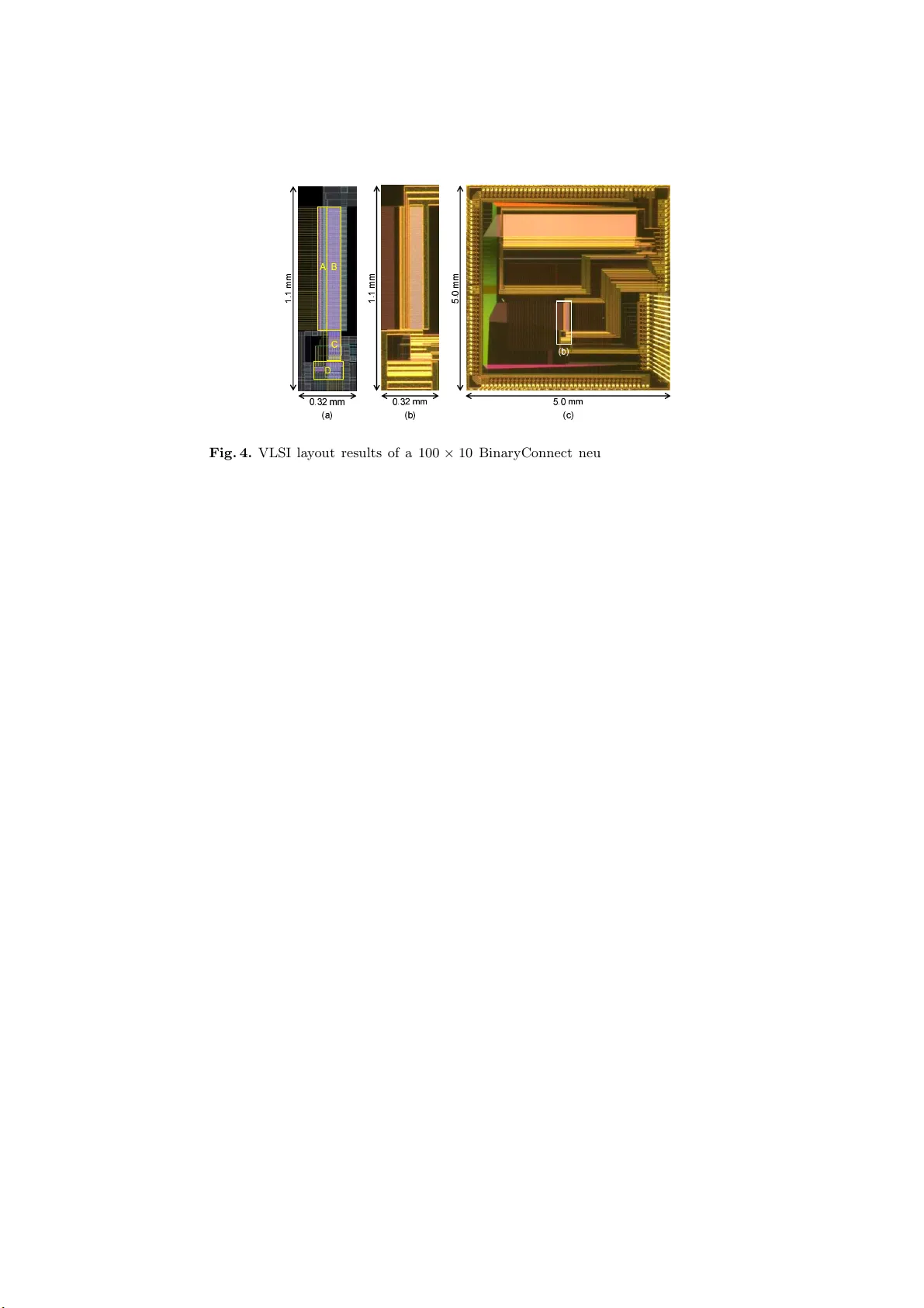
An Energy-efficien t Time-domain A nalog VLSI Neural Net w ork Pro cessor Based on a Pulse-width Mo dulation Approac h Masatoshi Y amaguchi, Goki Iwamoto, Hak aru T am ukoh, and T ak ashi Morie Graduate School of Life S cience and Systems Engineering, Kyushu Institute of T echnology 2-4, Hibikin o, W ak amatsu-ku, Kitakyu sh u, 808-01 96 Japan Abstract. A time-domain analog-weig hted-sum calculation mod el based on a pulse-width modulation (PWM) approach i s prop osed. The pro- p osed calculation mod el can b e applied to an y types of netw ork stru c- ture including multi-la yer feedforw ard netw orks. W e also propose v ery large-scale in tegrated (VLS I ) circuits to implement the proposed mo del. Unlike th e con ventional analog vol tage or curren t mode circuits used in computing-in-memory circuits, our time-domain analog circuits use tran- sien t operation in charging/disc harging processes to capacitors. Since the circuits can b e designed without op erational amplifiers, they can b e operated with ext remely low p ow er consumpt ion. How ever, they have to use v ery high- resistance devices, on the order of giga-ohms. W e de- signed a CMOS VLSI chip t o ve rify w eighted-sum op eration based on the prop osed mo del with b inary weigh ts, whic h realizes th e BinaryCon- nect mo del. In the chip, memory cells of static-random-access mem- ory (SRAM) are used for syn aptic conn ection w eights. High-resistance operation w as realized b y using the subt hreshold op eration region of MOS transistors unlik e the o rdinary computing-in-memory circuits. The chip w as designed and fabricated using a 250-nm fabrication technology . Measuremen t results sho w ed t hat energy efficiency for the weig hted- sum calculation was 300 TOPS/W (T era-Operations Per Second p er W att), which is more than one order of magnitude higher than that in state-of-the-art digital AI processors, even though the minimum width of in t erconnection used in this chip was several times larger than that in su c h digital pro cessors. If state- of-th e-art V LSI technology is used to implement t h e p rop osed mod el, an energy efficiency of more than 1,000 TOPS/W will be possible. F or practical applicati ons, developmen t of emerging analog memory devices such as ferroelectric-gate field effect transistors (F eFETs) is n ecessary . Keywords: time-domain analog computing, w eighted sum, multiply- and-accumulate, pulse-width mo dulation, deep neural n et w orks, multi- la yer p erceptron, artificial in telligence h ardw are, AI pro cessor 2 Masatoshi Y amaguc hi, Goki Iwamoto , Haka ru T amuk oh, T ak ashi Mori e 1 In t r o duction Artificial neural ne tw orks (ANNs), such as conv olutiona l deep neur a l netw o rks (CNNs) [12] and multi-lay er pe rceptrons (MLPs) [3], ha ve shown exce lle n t p er- formance on v arious tasks including imag e rec ognition [3 ,11,5,27,13]. How ever, computation in ANNs is very heavy , which leads to high p ow e r consumption in current digital computers and even in highly parallel copro cessor s suc h as graphics pro c e s sing units (GP Us). In o rder to implemen t ANNs at edg e devices such as mobile phones a nd p ersonal service rob ots, o per ation at very low p ow e r consumption is r equired. In ANN mo dels, weigh ted summation, or multiply-and-accumulate (MAC) op eration, is an esse ntial and heavy calculation task, a nd dedica ted comple- men tary metal-oxide-semiconductor (CMOS) v ery- la rge-sca le int egration (VLSI) pro cessor s have b e en developed to a ccomplish it [26,20,25,10,2]. As an imple- men tation approach other than digital pro cessors , use of a nalog oper ation in CMOS VLSI circuits is a promising metho d for achieving extremely low-power consumption for such calculation task s [6,14,19,17]. In pa rticular, computing-in- memory approaches, which a c hieve weigh ted-s um ca lculation utilizing the cir- cuit of static-ra ndom-access memory (SRAM), hav e b een p opular since ar ound 2016 [18]. Although the calculatio n precision is limited due to the non-idealities of ana - log op eration such a s noise and device mismatches, neural netw ork mo dels and circuits can b e designed to b e robust to such non-idealities [21,9,7]. On the other hand, ANN mo dels with binarized weights o r even with binarized inputs hav e been prop os ed and their comparable perfor mance has b een demonstrated, mainly in applications of image recognitio n [4,8]. These mo dels fac ilitate the developmen t of energy-efficient har dware implementations [19]. The time-domain ana log weigh ted- s um calculation mo del was or ig inally pro- po sed based on mathematical spiking neuron mo dels inspired by bio lo gical neu- ron b ehavior [15,16]. W e have s implified this calculation mo del under the as- sumption of oper ation in analo g circuits with tr ansient states, and call its VLSI implemen tation approa ch “Time-domain Ana lo g C o mputing with T r a nsient states (T A CT).” In c ont rast to conv entional w eighted-sum op era tio n in analog voltage or curre n t mo des, the T ACT approach is suitable for op era tio n with muc h low er power c onsumption in the CMOS VLSI implemen tation of ANNs. W e have already propo sed a device and circuit that per forms time-domain weigh ted-sum calculation [23,28,22]. The prop osed c ircuit consists o f plur a l in- put resistive elemen ts and a capac ito r (R C cir c uit), which can ac hieve extremely low-pow er op eration. The energy c onsumption could be lowered to the order of 1 fJ p er op era tion, whic h is almost comparable to the ca lculation efficiency in the brain, a s long a s weight ed-sum oper ation is consider ed. W e als o prop osed a circuit archit ecture to implemen t a weight ed-sum calculation with different- signed weigh ts with t wo sets of R C circuits, one o f whic h calcula tes positively weigh ted sums while the other calculates nega tiv ely w eighted sums [29,30]. Us- ing a similar time-domain appr oach, a vector-by-matrix m ultiplier using flash memory tec hno logy was propo sed [1]. An Energy-efficient Time-domain Analog VLS I N eural Pro cessor 3 I i I 1 Q C S i I 2 S 2 S 1 W i W 2 W 1 Fig. 1. W eigh t ed-sum calculation using current sources switched with PWM signals. W eighted-sum ca lculation circuits using puls e -width modula tion (PWM) sig- nals hav e previously b een pro po sed [24]. In this pap er, we reformulate the weigh ted-sum calculation mo del based o n the time-domain analog c o mputing approach using PWM signals , called the T ACT-PWM approach, and prop ose its applicatio ns to ANNs such as MLPs a nd CNNs with extremely high co mput- ing energy e fficie nc y . W e a lso s how the design and measurement re s ults of an ANN VLSI chip fabrica ted using a 250-nm CMO S VLSI tec hnology , in which the calculation results b y the pro po sed model are compared with the ordinary nu merical calculation results a nd verify its very high computing efficiency . 2 Time-domain weigh ted-sum calculation cir c uit mo del with PWM signals The basic circuit configura tio n based o n the T ACT-PWM approa ch is shown in Fig. 1. Corres po nding to input signals S i ∈ { 0 , 1 } in the voltage doma in, each switched-curren t so urce (SCS) outputs curr en t I i when S i = 1. An SCS can be replaced by a resisto r and a dio de if the nonlinearity in charging characteris tics can be ignored. The total charge amo unt Q sto r ed at the no de of ca pa citor C charged by N SCSs with inputs S i , ea ch of which has pulse width of W i , is expressed b y Q = N X i =1 W i I i , (1) where Q ca n b e considered as the weigh ted-sum calculation result with weight I i and input W i . The no de voltage of C , V c , is given by V c = Q /C . If I i ≥ 0 , the energ y consumption E of this c harging and discharging pro ces s is given b y E = C V c V dd ( V dd is a s upply voltage of SCSs), where the energy for c ha rging the input capa citance of SCSs is not included. The weigh ted-sum calcula tion circuit and a timing diagram of its op er ation are shown in Fig. 2. Here, w e consider this op eration a s a w eig h ted-sum calcu- lation with the same signed w eig hting. The circuit consis ts of a w eighted-sum calculation or MAC part a nd a voltage-pulse co n version (VPC) part. The MA C part co nsists of SCSs cor r esp onding with inputs, which is a ccompanied by pa r a- sitic wiring capac itance C d . The VPC part consists of an SCS, tw o sw itches, and a compa rator with an input ca pa citance C n . Since the par asitic capacitances C d 4 Masatoshi Y amaguc hi, Goki Iwamoto , Haka ru T amuk oh, T ak ashi Mori e and C n are inevitably included in the c ir cuit, to minimize the ene r gy consump- tion for the opera tion, the charged capacitance C , which is equa l to C d + C n , should be as small as p oss ible . The PWM inputs a re g iven in the input p erio d T in ; ∀ i, W i ≤ T in , whic h is arbitrar ily determined. If the node voltage V c at the timing of the end of this input perio d is denoted b y V mac , V mac = Q C d + C n = 1 C d + C n N X i =1 W i I i . (2) In the VPC part, the output P WM sig nal S out with pulse width W out is generated during the output perio d T out . In this op er ation, capacitance C is charged up by the SCS with current I n . T o minimize the energ y consumption in this op eration, the VPC par t can be separated from the MA C part by S n , and only C n can b e charged up to the threshold voltage V θ of the compar ator. In this ca se, to meet the condition that 0 ≤ W out ≤ T out , the current I n is given b y I n = C n V θ T out , (3) which means that the no de v o ltage V n increases with the slope of V θ /T out . When V n > V θ , the comparato r output S out = 1, and after the end of output p erio d V n is re s et b y S r st at the resting state, which is usually zero. Thus, the pulse width of the output signal as a result of w eig ht ed-sum calcula tion is given by W out = V mac V θ T out (4) = T out ( C d + C n ) V θ N X i =1 W i I i , (5) where it is ass umed that 0 ≤ Q ≤ ( C d + C n ) V θ . If the same input line structur es are used regar ding the positive and negative weigh ts, the denominator of Eq. (5) is co mmon, Thu s, positive and negative weigh ted ca lculations a re p erfor med sepa rately in the different lines, and by subtracting W out for negative weighing from that for the pos itiv e o ne, the total calculation result is o bta ined as follows: W + out − W − out = T out ( C d + C n ) V θ " N + X i =1 W + i I + i − N − X i =1 W − i I − i # , (6) N = N + + N − , (7) where W ± out are the pulse widths of output signals with p ositive a nd neg ative weigh ting, res pectively . Since the obtained result can b e fed into the next circuit corres p onding to the next layer of t he netw or k via nonlinear tra nsform op eratio n, calculations for ANNs can be achieved. An Energy-efficient Time-domain Analog VLS I N eural Pro cessor 5 S i I i S 1 I 1 S n I n S o u t V θ S rs t C d C n V n (a ) (b) t ime S n V n T out T in S out V θ 2 V θ S 3 W 3 S 2 W 2 S 1 W 1 W out MA C V PC Fig. 2. W eighted-sum calculation circuit mod el with the same signed w eighting: (a) circuit diagram and (b ) t iming diagram. The total energy consumption for the MAC calc ula tion is ex pressed as fol- lows: E cal = E mac + E vpc , (8) E mac = C d V mac V dd + N X i =1 E i , (9) E vpc = C n ( V mac + V θ ) V dd + E n + Z T in + T out 0 P cmp ( t ) dt, (10) where E mac and E vpc are the ener gy co ns umptions of the MA C and VPC parts, E i and E n are those for the switc hing of the SCS at ea ch MAC par t i and for the switchin g of the SCS at the VPC part, respec tively , and P cmp ( t ) is the pow er consumption of the compar ator. 6 Masatoshi Y amaguc hi, Goki Iwamoto , Haka ru T amuk oh, T ak ashi Mori e 3 CMOS B inaryConnect netw ork circuit based on T A CT-PWM approac h On the basis of o ur T ACT-PWM circuit appr oach, a CMOS circuit using an SRAM cell ar ray s tructure is shown in Fig. 3(a). This circuit implements a BinaryConnec t neural netw o rk, which uses ana lo g input v alues while weight s are binary [4]. This circuit co nsists of a syna pse pa rt and a neuron par t. The sy napse part consists of an SRAM cell ar ray , and each s ynapse circuit op erates as tw o MA C circuits. Unlike the ordina ry SRAM circuits pr o po sed in the concept of computing-in-memory , our SRAM cell circuit outputs very low c ur rent on the order of nano-amp eres to guarantee the time consta nt in the T ACT ap- proach [29,30], and therefore the p-type MO S field effect transistor s (pMOS- FETs) M ± supply subthreshold c urrents to dendrite lines D ± based on the input fro m axon lines A i , where axon and dendrite are neur oscientific terms in the biological neur on. In the neuron part, tw o VPC circuits perform positive and neg ative weigh ting calculations, resp ectively , and the subtraction result is fed int o a rectified-linea r- unit (ReLU) function circuit. A detailed explanation follows. 3.1 Synapse part In the synapse part, each SRAM cell shown in Fig . 3(b), whic h is called here a binary synapse unit (BSU), p erfor ms bina ry weight ing, when receiving an input pulse S i as the g ate v o ltage of the pMOSFET M ± to mak e it op era te in the subthreshold re g ion. T o p erfo r m this oper ation, it is necessary that the SRAM cell b e se t at a 0 o r 1 sta te ba sed on the training result in a BinaryConnect net work. The BSU has three functions: one- bit memory , a switched current source , and a selector. The one-bit memory function is achiev ed at the flip-flo p, whic h stores the binary weight w i ∈ { +1 , − 1 } b y setting v oltages V + P and V − P , a s follows: w i = { +1 if ( V + P , V − P ) = ( V dd , 0) − 1 if ( V + P , V − P ) = (0 , V dd ) , (11) where V dd is the supply voltage. The switched cur rent s ource with a selector is realized b y pMOSFETs M ± that are connected to dendrite lines D ± , respec - tively . Since pMOSFETs M ± op erate in the subthreshold region, their drain currents I ± i are expressed a s follows: I ± i ≈ I 0 exp( V ± P − V Ai ) (12) V Ai = V dd if S i = 0 V w if S i = 1 , (13) where I 0 is a constant, V Ai is the voltage of axon line A i , a nd V w is the co nstant gate voltage for subthreshold oper ation. F or e x ample, if synapse i has p o sitive weigh t ( w i = 1) and S i = 1, then ( V + P , V − P ) = ( V dd , 0), and I + w ≈ I 0 exp( V dd − V w ), and I − w ≈ 0. An Energy-efficient Time-domain Analog VLS I N eural Pro cessor 7 T out (b) (c) (d) (a) D − D + V dd V dd M + C di + C di − A i P − I i + I i − P + M − ReLU C n + C n − V θ V n − V n + I n − I n + W out − W out + W out S n S rst D − D + Neuron part Synapse part BSU BSU S 1 S i W i V w V w V dd V dd A i A 1 W 1 W out − W out + W out S out − S out + S out S out − S out + S out S out − S out + S out time Fig. 3. BinaryConnect neural netw ork circuit based on T ACT-PWM approac h : (a) sc hematic diagram, (b ) binary sy n apse un it (BSU) circuit, (c) ReLU fun ction circuit, and (d) timing diagra m of th e ReLU function circuit. 3.2 Neuron part In the neuro n circuit, dendrite lines ar e initialized and reset at gr ound lev el b y S r st befo re inputting signals S i to the synapse part. Next, input P WM signa ls are given during input time p erio d T in , and capacitance C di and C n are charged. Then, dendrite lines are separated b y neuron parts with S n . A t the same time, the current source I n is connected to capacita nce C n , and thus C n is charged. When the no de voltage of C n , V ± n , reaches the threshold voltage of the co mparator, the output signal S ± out is gener ated. A set o f output sig na ls S ± out are fed into the ReLU function c ircuit, which simply consists of logic circuits, as shown in Fig. 3(c), and the output PWM signal is only generated when W + out > W − out , as shown in Fig. 3 (d). 4 VLSI c hip design and measuremen t results Using TSMC 250 nm CMO S technology we designed and fabricated a CMOS VLSI chip of our neural net work circ uit with ten neurons each of w hich ha s 1 00 synapses. The layout results and micr o photogra phs a re sho wn in Fig . 4. 8 Masatoshi Y amaguc hi, Goki Iwamoto , Haka ru T amuk oh, T ak ashi Mori e T able 1. Measuremen t conditions and results for p o wer efficiency of the fabricated VLSI chip Number of synapses 100 × 10 Op erations p er syn apse 2 (MAC) Number of neurons 10 Input pulse width 300 n s Output pulse width 300 n s Supply voltage V dd 1 V Threshold voltag e V θ 0.2 V Op eration freq. 2.9E5 Hz Op erations/sec 5.9E8 OPS P o w er consumption 1.9E-6 W P o w er efficiency 3.0E14 O PS/W Measurement results of the input-output relationship in weigh ted-s um cal- culations op era tions at o ne neuron with 100 syna pses are s hown in Fig. 5. As shown in Fig. 5(a), weigh ted- sum o per ation was approximately achiev ed and sufficient linearity w a s o btained. F rom Fig. 5(b), the deviations in the time do- main ar e ± 20 ns, and this means that the pr e cision of the calculation is ab out ± 1 % b ecause of the ma xim um pulse width b eing 2 µ s. Ho wever, an offset and scattering of w eighting are clearly observed in Fig. 5(a). These nonidea lities are due to v ar iations in the thresho ld v o ltages of MOSFETs op erating in the sub- threshold region in BSUs. Such v a riations c an be comp ensated for by a djusting the threshold voltages if analog memo ry devices suc h a s ferro electric-g ate FETs are used in BSUs. Measurement res ults of the output pulse width as a function o f w eighted- sum calculation r esults followed b y the ReLU function in o ne neuro n with 100 synapses are shown in Fig. 6. The av e rage error w a s 1.5 %, a nd the maximum error was a b out 8 %. This erro r can b e decr eased by a djusting the de v iations of the threshold voltages of MOSFETs op erating in the subthr e s hold r egion. The measurement conditions and results for the p ow e r efficiency o f the fab- ricated VLSI c hip are s hown in T a ble 1 . The p ow er efficiency obtained from the measurement was 300 TO PS/W (T er a-Op eratio ns Per Second p er W att), which is ab out 30 times higher than that of state-o f- the- art digital AI proces sors, while the minim um feature size o f the VLSI fabrication tec hno lo gy use d w as around 10 times larger than that in the digital AI pro cessors. Therefor e, if w e used the same VLSI fabrication technology as in the digita l AI pro ces s ors, we could obtain a power e fficiency of mor e than 1,000 TOPS/W or 1 POPS/W (Peta-OPS/ W). 5 Conclusions In this pa per , we proposed a time-domain weigh ted- sum calculatio n mo del based on the T A CT- PWM appro ach with an activ ation function of ReLU. W e also An Energy-efficient Time-domain Analog VLS I N eural Pro cessor 9 ! " # $ % & ' ( ) * + , - . / Fig. 4. VLSI la yout results of a 100 × 10 BinaryConnect neural netw ork: (a) la yout result, (b) microphotograph of the circuit, and (c) chip microphotograph. A: switch and bu ffer arra y for axon lines, B: BSU array , C: n euron arra y , and D: bu ffer arra y for dendrite lines. prop osed VLSI circuits based on the T ACT a pproach to implemen t a calcula- tion model with extremely low e nergy co nsumption. A hig h energy efficiency of 300 TO PS/W was achiev ed by the fabricated CMOS VLSI circuit with binar y weigh ts using 250- nm CMOS VLSI technology . If w e use a more adv ance d VLSI fabrication technology , which achiev es lower parasitic capacita nc e , the energy efficiency will b e further muc h impro ved to over 1,000 TOPS/W. How ever, the fabricated circuit had insufficien t calculation precision, whic h is mainly due to the characteristic v ariations o f subthreshold op eration in MOS- FETs. T o improve the ca lculation pre c ision and compensa te for such v ar ia tions, it is ne c essary to introduce analog memory devices. As for the neuron parts, the measurement r esults of the fabricated VLSI c hip suggest that the ener gy consumption of this par t is comparable to that of the whole synapse par t with 1 00 inputs. Therefore, it is also neces sary to redesign a comparato r circuit with m uch low er p ower cons umption to improv e the ener gy efficiency of the whole calculation circuit. Ac knowledgmen ts. This work was suppor ted b y JSPS KAKENHI Grant Nos. 22240 022 and 15 H01706. Part of the w or k was carr ied o ut under a pr o ject com- missioned by the New E nergy and Industrial T echnology Dev elopment O rgani- zation (NEDO), and the Collabor ative Research Pr o ject of t he Institute of Fluid Science, T ohoku Universit y . The circuit design was supp or ted by VLSI Design and Education Center (VDEC), the Universit y of T okyo in collab oration with Cadence Design Systems, Inc., Mentor Graphics , Inc., and Synopsys, Inc. 10 Masatoshi Y amaguc hi, Goki Iwamoto , Haka ru T amuk oh, T ak ashi Mori e (a) (b) Input pulse width W i ( µ s) Output pulse width W out ( µ s) 2.5 2.0 1.5 1.0 0.5 0 0 1.0 2.0 + 100 0 − 100 0.5 1.5 Sum of all binary weights Deviation (ns) Measurement index + 40 + 20 0 − 20 − 40 0 1000 2000 3000 4000 5000 + 100 0 − 100 Sum of all binary weights Fig. 5. Measuremen t results of input-outpu t characteristics : (a) av eraged output pulse width and (b) dev iation. References 1. Ba va ndp our, M., Mahmoo di, M.R., Struko v , D.B.: Energy-efficient time- domain v ector-by-matrix multipli er for neuro computing and beyond. CoRR abs/1711. 10673 (2017), http://arxi v.org/abs /1711.10673 2. Bisw as, A., Chandrak asan, A .P .: Conv-RAM: An en ergy-efficient SRAM with em- b edded con volution computation for lo w-p o wer CNN-based machine learning ap- plications. In: IEEE Int. Solid-S tate Circuits Conf. ( I SSCC). pp . 488–489 (2018) 3. Cire ¸ san, D.C., Meier, U., Gambardella , L.M., Sc h midhuber, J.: Deep, big, simple neural nets for handwritten digit recognition. Neural Comp. 22(12), 3207–3220 (2010) 4. Courbariaux, M., Bengio, Y., Da vid, J.P .: Binaryconn ect: T raining deep neural netw orks with binary weigh ts durin g propagations. In: Adv ances in Neu ral I n for- mation Processing Systems. pp. 3123–3131 ( 2015) An Energy-efficient Time-domain Analog VLS I N eural Pro cessor 11 20 40 60 0 − 20 − 40 − 60 Ou tput puls e width W ou t ( µ s ) 2.5 2.0 1.5 1.0 0.5 0 Nu m erical res u lt of MA C o peration Fig. 6. Measuremen t results of output pu lse widths for the combination of random w eigh t s and inp u ts. Timing jitters were decreased by ave raging outpu t signals for 50 measuremen t results. The horizontal axis shows n u merical calculation va lues of P N =50 i =1 w i · W i /T i , where w i ∈ { +1 , − 1 } and 0 ≤ W i /T in ≤ 1 . 5. F arab et, C., Couprie, C., Na jman, L., LeCun, Y.: Learning h ierarc hical features for scene lab eling. IEEE T rans. P attern Analysis and Mac hine Intelligence 35(8), 1915–19 29 (2013) 6. Fic k , L., Blaauw , D., Sylv ester, D., S krzyniarz, S., Parikh, M., Fic k , D.: Analog in- memory su b threshold deep neural netw ork accelerator. In: Pro c. of IEEE Custom Integrated Circuits Conf. ( CICC). pp . 1–4 (2017) 7. Guo, X., Bay at, F.M., Prezioso, M., Chen, Y., Nguyen, B., Do, N., S truko v, D.B.: T emp erature-insensitive analog v ector-by-matrix multiplier based on 55 nm N OR flash memory cells . In: Pro c. of IEEE Custom In tegrated Circuits Conf. (CICC). pp. 1–4 (2017) 8. Hubara, I., Courbariaux, M., Soudry , D., El -Y aniv, R., Bengio, Y.: Quan t ized neu- ral netw orks: T raining neural netw orks with low precision w eigh ts and activ ations. J. Mac h . Learn. Res. 18(1), 6869–6898 (2017) 9. Indiveri, G.: Computation in neuromorphic analog VLS I systems. In: Proc. of Ital- ian W orksh op on N eu ral N ets (WIRN) . pp. 3–19 ( 2001) 10. Khwa , W.S., Chen , J.J., Li, J.F., Si, X ., Y ang, E.Y., Su n , X., Liu, R., Chen, P .Y., Li, Q., Y u, S., Chang, M.F.: A 65nm 4Kb algorithm-depend ent computing- in- memory SRA M un it-macro with 2.3 ns and 55.8 TOPS/W fully parallel produ ct- sum op eration for binary DNN edge pro cessors. In : IEEE I nt. Solid-State Circuits Conf. (ISSCC). pp. 496–498 (2018 ) 11. Krizh ev sky , A., Sut ske ver, I., Hin ton, G.E.: Imagenet classification with deep con- vol utional n eural netw orks. In: P ereira, F., Burges, C.J.C., Bo ttou, L. , W einberger, 12 Masatoshi Y amaguc hi, Goki Iwamoto , Haka ru T amuk oh, T ak ashi Mori e K.Q. (eds.) Advances in Neural In formation Processing Systems 25, pp. 1097–110 5. Curran Asso ciates, Inc. (2012) 12. Lecun , Y., Bottou, L., Bengio, Y ., Haffner, P .: Gradient-based learning applied to docu ment recognition. Pro c. IEEE 86(11), 2278–2324 (1998) 13. LeCun, Y., Bengio, Y ., Hin ton, G.: Deep learning. Nature 521(7553), 436–444 (2015) 14. Lee, E.H., W ong, S.S.: A 2.5 GHz 7.7 TOPS/W switc hed- capacitor matrix multi- plier with co-designed local memory in 40nm. In: I EEE Int. Solid-S tate Circuits Conf. (ISSCC). pp. 418–419 (2016 ) 15. Maass, W.: F ast sigmoidal net w ork s via spiking neurons. N eu ral Comp. 9, 279–304 (1997) 16. Maass, W.: Computing with spiking neurons. In: Maass, W., Bis hop, C.M. ( eds.) Pulsed Neural Netw orks. pp. 55–8 5. MI T Press (1999) 17. Mahmo o di, M.R., St ru ko v, D.: An ultra-lo w energy internally analog, externally digital vector-matrix m u ltiplier based on N OR flash memory technology . In: Pro c. of Design Automation Conf. ( DA C). p. 22 (2018) 18. Milo jicic, D., Bresniker, K., Campbell, G., F araboschi, P ., Strachan, J.P ., Wi lliams, S.: Computing in-memory , Revisited. In: I EEE 38th International Confere nce on Distributed Computing Sy stems (ICDCS). pp. 1300–1309 ( 2018) 19. Miyashita, D., Kousai, S., Suzuki, T., Deguchi, J.: A n euromorphic c h ip opti- mized for deep learning and CMOS technology with time-domain analog and digital mixed-signal pro cessing. IEEE J. S olid-State Circuits 52(10), 2679–2689 (2017) 20. Mo ons, B., Uytterho even, R., Deh aene, W., V erhelst, M.: ENVISI ON: a 0.26-to- 10TOPS/W subw ord- parallel dynamic-voltag e-accuracy-frequency- scalable convo - lutional neural netw ork processor in 28nm FDSOI. In: IEEE In t. Solid-S tate Cir- cuits Conf. (ISSCC). pp . 246–247 (2017) 21. Morie, T., A memiya , Y.: An all-analog ex pandable n eural netw ork LSI with on- c hip backpropagati on learning. IEEE J. S olid-State Circuits 29(9), 1086 –1093 (199 4) 22. Morie, T., Liang, H., T ohara, T., T anak a, H., Igarashi, M., Samuk a w a, S., End o, K., T ak ahashi, Y.: S p ike-based time-domain w eighted-sum calcula tion using nan- odev ices for lo w pow er op eration. In: 16th Int. Conf. on N anotec hnology (IEEE NANO). pp. 390–392 ( 2016) 23. Morie, T., Su n , Y., Liang, H., Igarashi, M., Huang, C., Samuk aw a, S.: A 2- dimensional Si nano disk arra y structure for spiking neuron mo dels. In: IEEE Pro c. of Int. Symp. Circuits and Systems (IS CAS). p p. 781–784 (2010) 24. N agata, M., F un ak oshi, J., Iwa ta, A.: A PWM signal pro cessing core circuit b ased on a switc hed current integration tec hn ique. IEEE J. Solid-S tate Circuits 33(1), 53–60 (1998) 25. S hin, D., Lee, J., Lee, J., Y oo, H.: DNPU: An 8.1TOPS/W reconfigurable CNN- RNN pro cessor for g eneral-purp ose deep neu ral net works. I n: IEEE Int. Solid-State Circuits Conf. (ISSCC). pp. 240–241 ( 2017) 26. S im, J., P ark, J.S., Kim, M., Bae, D., Choi, Y., Kim, L.S.: A 1.42T OPS/W deep conv olutional n eural netw ork recognition p ro cessor for intellig ent IoE systems. I n: IEEE Int. Solid-State Circuits Conf. (IS SCC). pp. 264–265 (2016) 27. S zegedy , C., Liu, W., Jia, Y., Sermanet, P ., Reed, S., Anguelo v , D., Erhan, D ., V anh ouc ke, V., Rabinovic h, A.: Going deeper with co nv olutions. In: Proc. of IEE E Conf. on Computer Vision and P attern R ecognition (CVPR). p p. 1–9 (2015) 28. T ohara, T., Liang, H ., T anak a, H., Igarashi, M., Samuk aw a, S., End o, K., T ak a- hashi, Y ., Morie, T.: Silicon nano disk arra y with a fin field-effect transistor for time-domain w eigh t ed sum calculation t ow ard massiv ely parallel spiking neural netw orks. App l. Phys. Express 9, 03420 1–1–4 (2016 ) An Energy-efficient Time-domain Analog VLS I N eural Pro cessor 13 29. W ang, Q., T am u ko h, H., Morie, T.: Time-domain w eighted-sum calculation for ultimately low p o w er VLSI neural n etw orks. In: Proc. Int. Conf. on Neural Infor- mation Processing (ICONIP). pp. 240–247 (2016) 30. W ang, Q., T am ukoh, H., Morie, T.: A time-domain analog weig hted-sum calcu- lation model for extremely low p ow er VLS I implementation of m u lti-la yer neural netw orks. CoRR abs/1810.068 19 (2018), http://arxiv.org/a bs/1810.06 819
Original Paper
Loading high-quality paper...
Comments & Academic Discussion
Loading comments...
Leave a Comment