The effects of an atomistic interface roughness in n-type silicon nanowire transistors (SiNWT) on the radio frequency performance are analyzed. Interface roughness scattering (IRS) is statistically investigated through a three dimensional full-band quantum transport simulation based on the sp3d5s?* tight-binding model. As the diameter of the SiNWT is scaled down below 3 nm, IRS causes a significant reduction of the cut-off frequency. The fluctuations of the conduction band edge due to the rough surface lead to a reflection of electrons through mode-mismatch. This effect reduces the velocity of electrons and hence the transconductance considerably causing a cut-off frequency reduction.
Since the lengths of silicon (Si) metal-oxidesemiconductor field effect transistor (MOSFET) have been scaled down to the sub-100 nm regime, the cutoff frequency has increased significantly to reach hundreds of gigahertz (GHz) [1][2][3] . Even though the cut-off frequency is not the only important parameter in radio frequency (RF) MOSFETs, a high cut-off frequency certainly represents a good criterion for Si MOSFETs to catch up with III-V transistors if other shortcomings are overcome. Power losses due to a long skin depth of the Si substrate, a poor noise figure and a high gate resistance 4 are the examples of such obstacles. Recently there have been tremendous efforts to improve the RF performance of the Si MOSFET and it is becoming competitive to III-V high electron mobility transistor (HEMT)/heterojunction bipolar transistor (HBT) or silicon germanium (SiGe) HBT 2,3,5 .
Silicon-on-insulator (SOI) multi-gate (MG) structures also have been found to be capable of achieving the cutoff frequency predicted by the international technology roadmap for semiconductors (ITRS) 6 for RF applications while reducing substrate losses and noise figures 7 . Gateall-around (GAA) siicon nanowire transistors (SiNWTs) have attracted attention since it was found that their cutoff frequency can be much larger than that of planar Si MOSFET 8 .
Traditionally, interface roughness scattering (IRS) has been considered as one of the most important scattering mechanisms. At a high effective electric field, IRS dominates the universal mobility trend 10 . In SiNWTs, IRS is still an important scattering mechanism reducing the oncurrent and the mobility significantly from the ballistic values 11 . a) Electronic mail: kim568@purdue.edu. This paper focuses on the effects of interface roughness scattering on the RF performance of SiNWTs, especially on the cut-off frequency (f T ). For that purpose, a three dimensional full-band quantum transport simulator based on the sp 3 d 5 s * tight-binding (TB) model 12,13 is used. As the maximum oscillation frequency (f max )another important figure of merit of the RF MOSFETs is directly related to the cut-off frequency 8 , the effects of IRS on the theoretical limit of the SiNWT’s RF performance can be estimated through this study.
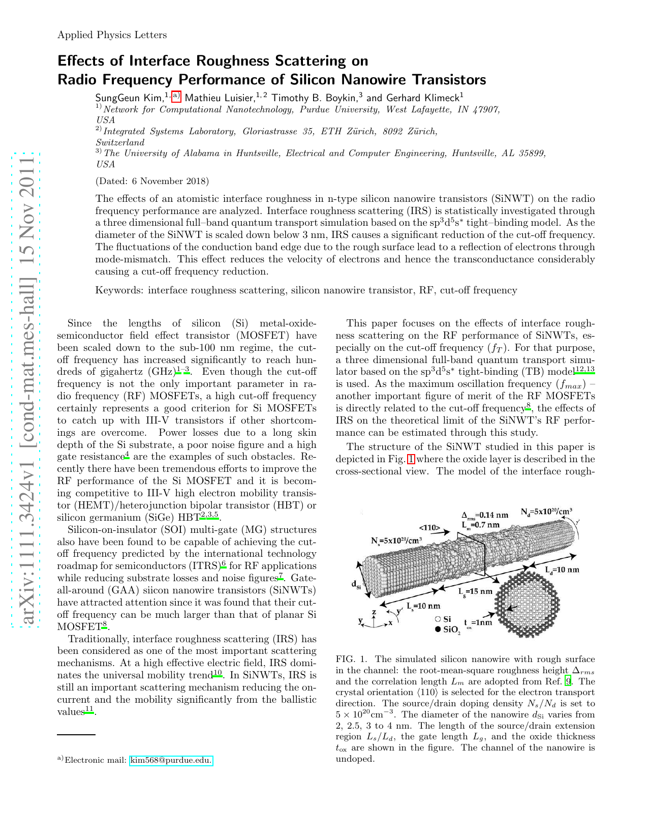
The structure of the SiNWT studied in this paper is depicted in Fig. 1 where the oxide layer is described in the cross-sectional view. The model of the interface rough- ness in the SiNWT used in the simulation is described in Ref. 11 where the influence of the interface roughness scattering on the direct-current (DC) characteristics of SiNWTs is presented. The silicon dioxide (SiO 2 ) layer is included in the transport calculation 11 to accurately model the wavefunction penetration into the oxide layer.
The cut-off frequency f T is related to the transconductance g m,on and the total gate capacitance C g,tot through the relationship
where g m,on and C g,tot are calculated through the following expressions at the on-state defined by the gate voltage V gs at V th + 2/3V dd 14 :
where V th is the threshold voltage, V dd the supply voltage and N 1D the total electron density under the gate divided by the gate length. The threshold voltage V th is determined using a critical current
The simulated cut-off frequency of a smooth nanowire (NW) is shown in Fig. 2(a). The results obtained here are similar to the data calculated in Ref. 8. The cut-off frequency increases as the nanowire diameter decreases. This is to first order a consequence of the improvement of the injection velocity in a 110 silicon nanowire (SiNW) with smaller diameter 15 .
As shown in Fig. 2(b), the transconductance g m,on is reduced significantly by the IRS while C g,tot is not affected much (Fig. 2(c)). The reduction of g m,on is due to reflections caused by the rough interface. A small dip in g m marked by an arrow in Fig. 2(d) is an indication that the second subband starts to carry the current 16 . In rough NWs, this dip is smoothed out due to subband mixing.
Mismatches of the subbands throughout the channel of the rough nanowire also can be observed in Fig. 3(b). This causes reflections of electrons causing reduction of the electron velocity which, in turn, reduces the transconductance. Fig. 4(b) shows the electron velocity throughout the smooth NW and the rough NWs with the diameter 2nm. The electron velocity is significantly reduced by interface roughness scattering.
One thing noticeable in Fig. 4(b) is that the IRS causes a reduction of the electron velocity at the beginning of the channel, but not much at the end of the channel. Electrons gain a relatively large kinetic energy due to a large electric field at the end of the channel. As a result, the fluctuation of the conduction band edge at the end of the channel does not affect the electron velocity significantly.
The cut-off frequency relationship (Eq. 1) can also be expressed as
Therefore, the average electron velocity v on can be calcu
This content is AI-processed based on open access ArXiv data.