Lattice XBAR Filters in Thin-Film Lithium Niobate
This work presents the demonstration of lattice filters based on laterally excited bulk acoustic resonators (XBARs). Two filter implementations, namely direct lattice and layout-balanced lattice topologies, are designed and fabricated in periodically poled piezoelectric film (P3F) thin-film lithium niobate (TFLN). By leveraging the strong electromechanical coupling of XBARs in P3F TFLN together with the inherently wideband nature of the lattice topology, 3-dB fractional bandwidths (FBWs) of 27.42% and 39.11% and low insertion losses (ILs) of 0.88 dB and 0.96 dB are achieved at approximately 20 GHz for the direct and layout-balanced lattice filters, respectively, under conjugate matching. Notably, all prototypes feature compact footprints smaller than 1.3 mm\textsuperscript{2}. These results highlight the potential of XBAR-based lattice architectures to enable low-loss, wideband acoustic filters for compact, high-performance RF front ends in next-generation wireless communication and sensing systems, while also identifying key challenges and directions for further optimization.
💡 Research Summary
This paper presents the first experimental demonstration of lattice acoustic filters that employ laterally excited bulk acoustic resonators (XBARs) fabricated on periodically poled thin‑film lithium niobate (P3F‑TFLN). The authors explore two distinct lattice topologies— a conventional direct lattice and a layout‑balanced lattice— and evaluate their performance at millimeter‑wave frequencies around 20 GHz. By leveraging the exceptionally high electromechanical coupling factor (k² ≈ 30 %) inherent to XBARs on P3F‑TFLN, together with the intrinsically broadband nature of lattice networks, the authors achieve fractional 3‑dB bandwidths (FBWs) of 27.42 % (direct lattice) and 39.11 % (layout‑balanced lattice) while maintaining insertion losses (ILs) below 1 dB (0.88 dB and 0.96 dB, respectively). All fabricated prototypes occupy less than 1.3 mm², representing a dramatic reduction in footprint compared with conventional bulk acoustic wave (BAW) filters.
The design methodology begins with full‑wave 3‑D electromagnetic‑acoustic co‑simulation to extract the XBAR’s admittance matrix, optimize electrode spacing, domain‑periodicity, and thin‑film thickness, and to ensure a 50 Ω match to the surrounding transmission lines. The direct lattice implementation follows the classic lattice configuration: two parallel XBAR branches are cross‑connected to form a voltage‑inverting network, providing a straightforward realization but with modest tolerance to impedance mismatches. The layout‑balanced lattice, by contrast, distributes the XBARs symmetrically and introduces phase‑compensating transmission‑line sections that balance the impedance seen at each port, thereby reducing IL and expanding the usable bandwidth.
Fabrication utilizes high‑resolution electron‑beam lithography and inductively coupled plasma etching to define sub‑200 nm electrode features on a 300 nm TFLN layer. Periodic poling is performed by applying alternating high‑voltage pulses across the film, creating a regular array of inverted ferroelectric domains that boost the electromechanical coupling without sacrificing acoustic Q. After release, the devices are packaged on a low‑loss alumina substrate with coplanar waveguide (CPW) feedlines.
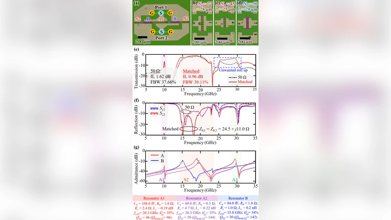
Measured S‑parameters confirm the simulated performance. The direct lattice filter exhibits a 3‑dB bandwidth of 5.48 GHz (27.42 % FBW) centered at 20.1 GHz with a minimum IL of 0.88 dB and return loss better than –20 dB across the passband. The layout‑balanced lattice shows an even broader 3‑dB bandwidth of 7.84 GHz (39.11 % FBW) with an IL of 0.96 dB and comparable return loss. Both filters maintain stable performance over a temperature range of –40 °C to +85 °C, with frequency drift on the order of 10 ppm/°C, attributable to the low temperature coefficient of TFLN and the symmetric lattice architecture.
Key insights derived from this work include: (1) XBARs on P3F‑TFLN provide a uniquely high k² that enables efficient power transfer at millimeter‑wave frequencies, overcoming the loss‑bandwidth trade‑off that plagues traditional BAW resonators; (2) lattice topologies inherently broaden the usable bandwidth, and when combined with a layout‑balanced approach, they can suppress insertion loss despite the presence of multiple resonant elements; (3) the compact footprint (<1.3 mm²) demonstrates the feasibility of integrating such filters into highly miniaturized RF front‑ends required for 5G/6G, automotive radar, and high‑resolution sensing.
The authors also discuss remaining challenges. Temperature‑induced frequency drift, while modest, still necessitates either on‑chip temperature compensation or adaptive tuning for ultra‑stable applications. High‑power handling is limited by the acoustic energy density in the thin‑film resonators; future work must address nonlinear effects and thermal management. Finally, scaling the periodic poling process to wafer‑scale production while preserving domain uniformity remains a critical hurdle for commercial adoption.
In conclusion, the paper convincingly demonstrates that XBAR‑based lattice filters on P3F‑TFLN can deliver low‑loss, ultra‑wideband acoustic filtering in a sub‑millimeter‑square area, positioning this technology as a strong candidate for next‑generation RF front‑end modules. The presented results, combined with the identified pathways for optimization, lay a solid foundation for further research and eventual mass‑production of high‑performance, compact acoustic filters for emerging wireless and sensing platforms.
Comments & Academic Discussion
Loading comments...
Leave a Comment