Beyond One-Thousandth Energy Resolution with an AlMn TES Detector
The superconducting Transition-Edge Sensor (TES) is a critical technology for next-generation X-ray spectrometers, known for its exceptional energy resolution. In the last decade, TESs based on AlMn alloy films have been extensively used in several cosmic microwave background (CMB) experiments. The advantages of simple fabrication process and easily tunable critical temperature make them an alternative to bilayer TESs. However, they have rarely been applied to X-ray detection until now. We developed an annular AlMn TES for X-ray detection and tested it in a dilution refrigerator with a Superconducting Quantum Interference Device (SQUID) amplifier, achieving an Full Width at Half Maximum (FWHM) of 12.1 +- 0.3 eV at 17.48 keV. To the best of our knowledge, this is the first demonstration of an AlMn TES achieving an energy resolution below 0.1%, highlighting its potential for high-resolution X-ray detection.
💡 Research Summary
The paper reports the first demonstration of sub‑0.1 % (i.e., better than one‑thousandth) energy resolution using an aluminum‑manganese (AlMn) transition‑edge sensor (TES) for X‑ray detection. AlMn TESs have become popular in cosmic‑microwave‑background (CMB) experiments because their fabrication is simple and their critical temperature (Tc) can be tuned by a short anneal, but they have rarely been applied to X‑ray microcalorimetry.
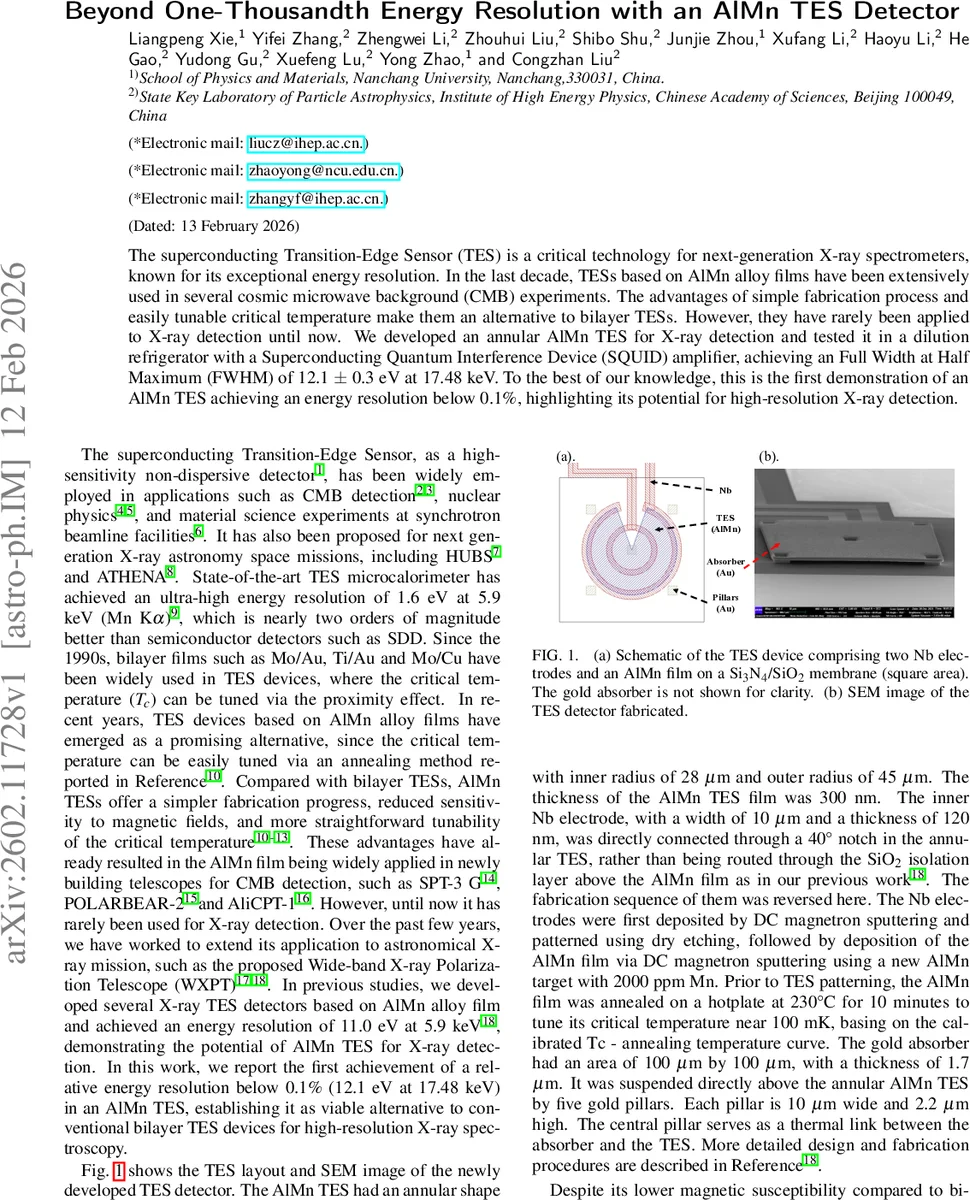
The authors fabricated an annular AlMn TES on a Si₃N₄/SiO₂ membrane. The AlMn film is 300 nm thick, contains 2000 ppm Mn, and was annealed at 230 °C for 10 min to set Tc≈100 mK. The TES has an inner radius of 28 µm and an outer radius of 45 µm; a gold absorber (100 µm × 100 µm × 1.7 µm) is suspended above it by five gold pillars, the central pillar providing the thermal link. Nb electrodes are deposited first and directly contact the TES through a 40° notch, eliminating an insulating SiO₂ layer used in earlier work.
Magnetic shielding is a critical part of the design. A composite shield consisting of a 1.5 mm Cryoperm 10 cover plate and a 2 mm Nb bottom plate reduces the ambient geomagnetic field to ≈1.35 µT at the TES and 0.45 µT at the SQUID, a factor of ~40 improvement over a pure Nb shield. COMSOL simulations and measurements confirm the effectiveness of the combined high‑permeability and superconducting layers.
The detector was mounted in a Bluefors LD250 dilution refrigerator and read out with a two‑stage SQUID from STAR Cryoelectronics. A 0.3 mΩ shunt resistor and a 200 nH series inductor (total series L = 230 nH) limit high‑frequency noise. The TES was biased at 0.385 V, corresponding to 48 % of its normal resistance (Rn ≈ 8.3 mΩ) at a bath temperature of 74 mK. From I‑V curves the thermal conductance G≈220 pW/K and loop gain L≈2.2 were extracted; the temperature and current sensitivities were αI = 13.7 and βI = 0.3, respectively. Pulse analysis gave an intrinsic decay time τ≈3 ms and a total heat capacity of 0.6 pJ/K, about five times larger than the calculated value, likely due to energy deposition in the Si substrate and a broadened superconducting transition caused by the annealing temperature.
X‑ray spectra were obtained using a Mini‑X2 tube illuminating Mn, Cu, Pb and Mo targets. After matched filtering, the pulse amplitudes were calibrated with a quadratic function. Voigt fits to the Mn Kα (5.9 keV), Cu Kα (8.0 keV), and Mo Kα (17.48 keV) lines yielded full‑width‑half‑maximum (FWHM) energy resolutions of 8.1 ± 0.6 eV, 11.4 ± 0.3 eV, and 12.1 ± 0.3 eV, respectively. The 17.48 keV result corresponds to a relative resolution of 0.069 % (0.69 ‰), the first sub‑0.1 % performance reported for an AlMn TES.
Noise measurements show that the observed resolution is limited by excess noise well above the theoretical limit of ≈3.4 eV (Johnson, thermal‑fluctuation, and SQUID noise). The authors attribute the excess to high‑frequency electromagnetic interference, noise from the room‑temperature voltage source, and thermal fluctuations caused by high‑energy photons depositing energy in the silicon membrane.
To improve performance, the paper suggests several avenues: keep the AlMn anneal temperature below 200 °C to avoid transition broadening; redesign the TES geometry to reduce current‑density non‑uniformity (e.g., increase the inner‑to‑outer radius ratio or adopt a rectangular shape); enhance electromagnetic shielding of the readout electronics; add low‑pass filtering at the mixing‑chamber stage; and reduce the X‑ray beam spot to limit substrate heating. With these refinements, the authors anticipate reaching the fundamental limit of 1–2 eV, comparable to state‑of‑the‑art bilayer TESs.
In summary, the work demonstrates that AlMn TESs, when combined with optimized magnetic shielding and careful thermal design, can achieve ultra‑high energy resolution at keV energies, opening the path for their use in future high‑resolution X‑ray astronomy missions (e.g., the proposed Wide‑band X‑ray Polarization Telescope) and synchrotron‑based material‑science applications.
Comments & Academic Discussion
Loading comments...
Leave a Comment