Analysis of Edge Mismatch and Output Power Degradation in Cascoded Class-D Power Amplifiers Using Dual-Range Voltage Level Shifters
This paper presents a low-jitter hybrid voltage level shifter (HVLS) suitable for high-speed applications. The proposed architecture offers the advantage of cross-coupled feedback to simultaneously generate two voltage domain signals with available swings equal to the nominal supply and its double, which operate up to 12.4 GHz. A prototype HVLS circuit, along with impedance matching and a driver to enable high-speed off-chip testing, was fabricated in a 22-nm FD-SOI process technology. The prototype consumes a total die area, including the interface circuitry, of 477 x 462 um^2, while the active area of the level-shifter is 2 x 3.26 um^2. The average power consumption of the circuit is measured to be 4.43 uW per cycle, and the jitter is less than 150 fs-rms.
💡 Research Summary
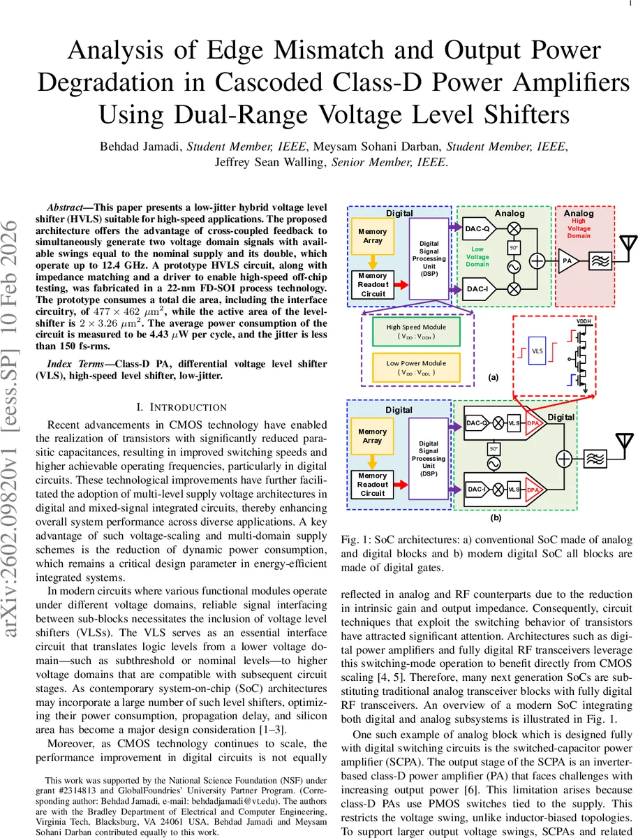
This paper addresses two intertwined challenges in modern mixed‑signal SoCs: (i) the limitations of conventional voltage level shifters (VLS) when operating at multi‑gigahertz frequencies, and (ii) the degradation of output power in cascoded class‑D power amplifiers (PA) caused by timing mismatch between the PMOS and NMOS drive signals.
First, the authors review three classic VLS topologies—Differential‑Cascade VLS (DCVS), Current‑Mirror VLS (CM), and Wilson‑Current‑Mirror VLS (WCMLS)—using a 22‑nm fully‑depleted silicon‑on‑insulator (FD‑SOI) process. Simulations reveal that DCVS offers high speed but suffers from large contention currents; CM provides fast switching at the cost of significant static power; WCMLS minimizes leakage but is limited to a few megahertz because its output current is too small. From these observations the authors extract five design criteria: minimal contention, fast transition at low input voltage, zero static current, compact area, and scalable delay with converging supply levels.
To overcome the identified shortcomings, the paper proposes a Hybrid Voltage Level Shifter (HVLS). The HVLS combines a cross‑coupled PMOS latch (providing regenerative pull‑up) with a current‑limiting transistor that suppresses the pull‑up current when the output is high. This architecture simultaneously generates two output levels, VDD and 2·VDD, from a single low‑voltage input, thereby eliminating the need for separate delay chains or calibration circuits.
The HVLS is fabricated in a 22‑nm FD‑SOI process. The active shifter occupies only 2 × 3.26 µm²; the full test chip (including matching network and driver) measures 477 × 462 µm². Measured performance shows operation up to 12.4 GHz, an average power consumption of 4.43 µW per clock cycle, and jitter below 150 fs‑rms. Compared with the conventional VLS families, the HVLS reduces power by one to two orders of magnitude while extending the usable frequency range by a similar factor.
The second major contribution is a rigorous analysis of delay mismatch in cascoded class‑D PAs. The authors first consider an ideal switch model, deriving the output power for a perfectly synchronized drive as
P_out,i = (8/π²)·VDD² / R_opt
and then introduce a timing offset δt = T_ms / T_c, which yields a degraded power
P_out,ni = P_out,i·
Comments & Academic Discussion
Loading comments...
Leave a Comment