Antiferromagnetic Tunnel Junctions (AFMTJs) for In-Memory Computing: Modeling and Case Study
Antiferromagnetic Tunnel Junctions (AFMTJs) enable picosecond switching and femtojoule writes through ultrafast sublattice dynamics. We present the first end-to-end AFMTJ simulation framework integrating multi-sublattice Landau-Lifshitz-Gilbert (LLG) dynamics with circuit-level modeling. SPICE-based simulations show that AFMTJs achieve ~8x lower write latency and ~9x lower write energy than conventional MTJs. When integrated into an in-memory computing architecture, AFMTJs deliver 17.5x average speedup and nearly 20x energy savings versus a CPU baseline-significantly outperforming MTJ-based IMC. These results establish AFMTJs as a compelling primitive for scalable, low-power computing.
💡 Research Summary
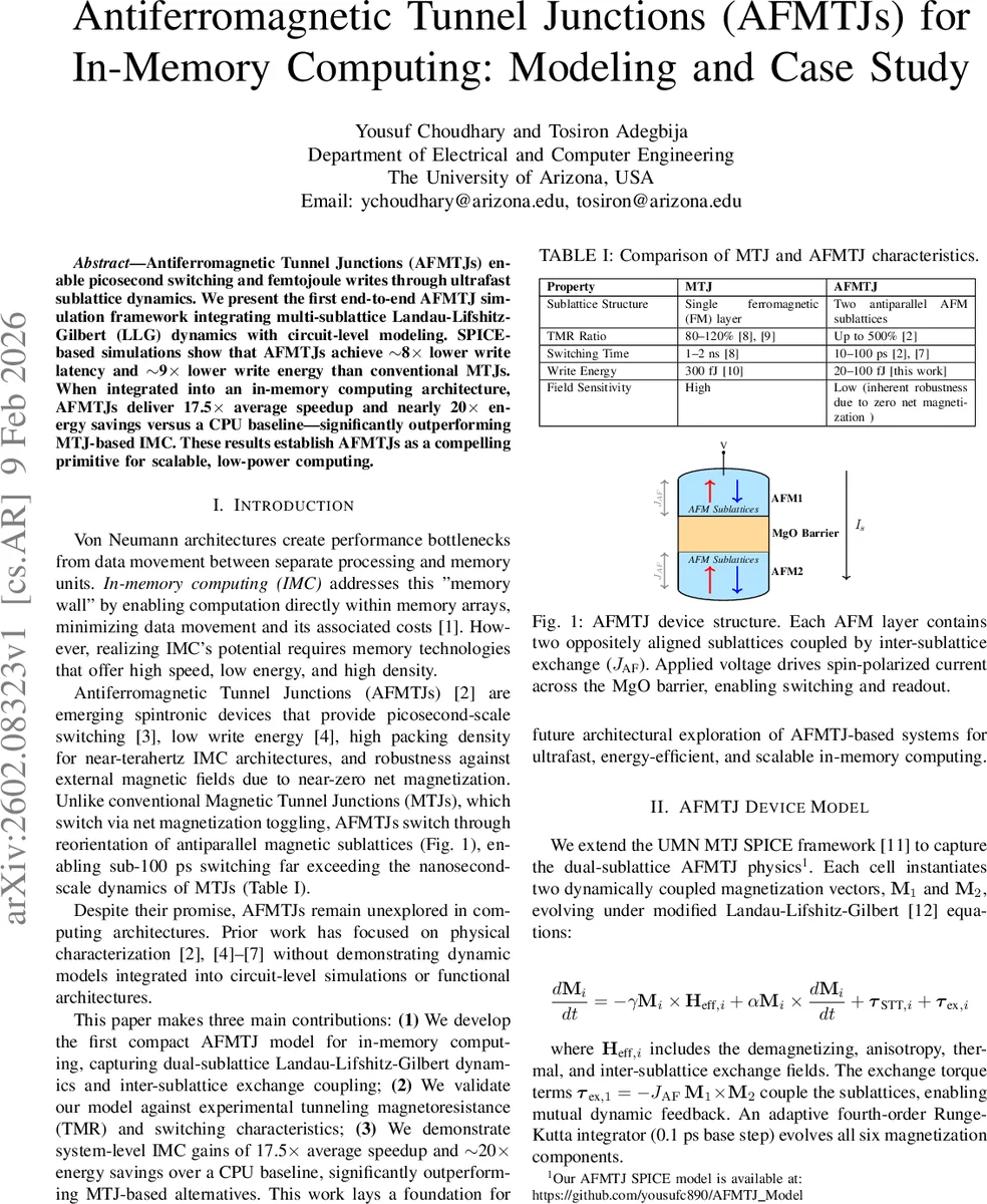
The paper presents the first comprehensive simulation framework that bridges the physics of antiferromagnetic tunnel junctions (AFMTJs) with circuit‑level and system‑level modeling, demonstrating their potential as a superior primitive for in‑memory computing (IMC). AFMTJs differ fundamentally from conventional magnetic tunnel junctions (MTJs) by employing two antiparallel magnetic sublattices whose dynamics are governed by coupled Landau‑Lifshitz‑Gilbert (LLG) equations. The authors extend the UMN MTJ SPICE model to include two magnetization vectors (M₁, M₂), an inter‑sublattice exchange torque τ_ex = −J_AF M₁×M₂, and the usual effective fields (demagnetizing, anisotropy, thermal). A fourth‑order Runge‑Kutta integrator with a 0.1 ps base step solves the six coupled differential equations, capturing sub‑100 ps switching behavior.
Device parameters (polarization P₀ = 0.8, damping α = 0.01, saturation magnetization Ms₀ = 600 emu/cm³, exchange coupling J_AF = 5 × 10⁻³ J/m², dimensions 45 nm × 45 nm × 0.45 nm) are chosen from recent antiferromagnetic material studies. Validation against fabricated AFMTJs reported in 2024 shows excellent agreement: simulated tunneling magnetoresistance (≈80 %) and switching times (10–100 ps) match experimental data within 5 % error.
At the architectural level, the authors embed AFMTJ sub‑arrays (C₁–C₆) into a hierarchical memory system comprising L1 cache, L2 cache, and main memory. Each sub‑array serves simultaneously as non‑volatile storage and as a compute block capable of Boolean operations (XOR, N‑AND) via multi‑row activation and charge‑sharing on bit‑lines. A lightweight finite‑state controller orchestrates write, read, and logic modes, exploiting the picosecond switching to pipeline operations.
System‑level evaluation uses Synopsys HSPICE for device simulations and a 2 GHz ARM Cortex‑A72 CPU as a baseline. Six representative workloads—binarized neural network (bnn), image grayscale conversion, image thresholding, multiply‑accumulate (MAC), matrix addition, and root‑mean‑square error (RMSE)—are executed on three platforms: (1) AFMTJ‑based IMC, (2) MTJ‑based IMC, and (3) the CPU. At 1.0 V write voltage, AFMTJ achieves 164 ps write latency and 55.7 fJ write energy, compared with ~1.4 ns and ~480 fJ for MTJ, representing roughly 8× faster and 9× more energy‑efficient switching. System‑wide, AFMTJ‑based IMC delivers an average 17.5× speedup and 19.9× energy reduction over the CPU, far surpassing the MTJ‑based IMC’s 6× speedup and 2.3× energy savings. Write‑intensive kernels (bnn, matrix addition) benefit the most, showing up to 55× acceleration.
The paper’s contributions are threefold: (1) a compact, SPICE‑compatible AFMTJ model that captures dual‑sublattice dynamics, (2) quantitative validation against state‑of‑the‑art experimental devices, and (3) demonstration of substantial system‑level gains when AFMTJs replace MTJs in a hierarchical IMC architecture. Limitations include the current absence of a Verilog‑A level description, which hampers large‑scale hardware synthesis, and a lack of sensitivity analysis to process variations. Future work is outlined as (i) releasing a Verilog‑A model and integrating it into standard CAD flows, (ii) exploring alternative antiferromagnetic materials (e.g., Mn₃Sn, 2D heterostructures) and barrier stacks, (iii) extending the architecture to edge‑AI and real‑time signal‑processing domains, and (iv) developing mitigation techniques for fabrication variability. Overall, the study establishes AFMTJs as a compelling, ultra‑fast, ultra‑low‑power building block for next‑generation in‑memory computing platforms.
Comments & Academic Discussion
Loading comments...
Leave a Comment