Exploring the Design and Measurements of Next-Generation 4H-SiC LGADs
This contribution presents the design, production, and initial testing of newly developed 4H-SiC Low Gain Avalanche Detectors (LGADs). The evaluation includes performance metrics such as the internal gain layer’s efficiency in enhancing signal generation. Initial laboratory and Transient Current Technique (TCT) measurements provide insight into the device’s stability and response to the signal. Due to the increase of availability provided by the industry, 4H-SiC is emerging as a strong candidate for the next-generation of semiconductor detectors. Such sensors are promising due to the inherent radiation tolerance of 4H-SiC and its stable operation across a wide temperature range. However, due to the wider-bandgap of 4H-SiC compared to standard silicon, and difficulty to produce high-quality layers thicker than 50 \textmu m, an internal charge multiplication layer needs to be introduced. The presented 4H-SiC LGADs, fabricated by onsemi, are optimized for an N-type substrate and epi wafer. The initial TCT and laboratory test results demonstrate fast charge collection and uniform multiplication across multiple samples produced on a single wafer.
💡 Research Summary
This paper reports on the design, fabrication, and initial characterization of Low‑Gain Avalanche Detectors (LGADs) built on 4H‑SiC substrates, a material that is gaining attention for its exceptional radiation hardness and wide‑temperature operation. Because 4H‑SiC has a large band‑gap (≈3.26 eV), the intrinsic charge generated by ionizing particles is much lower than in silicon, and thick, high‑quality epitaxial layers (>50 µm) are difficult to obtain. To compensate, the authors introduced a thin (≈1 µm) highly doped gain layer near the front surface, creating an internal avalanche region that provides moderate charge multiplication while preserving fast timing.
The devices were produced by onsemi on 6‑inch N‑type 4H‑SiC wafers with 30 µm and 50 µm epitaxial layers separated from the substrate by a heavily doped buffer. Each wafer contained three device types: a standard PN diode (no gain), LGAD1 with a lower gain‑layer doping, and LGAD2 with a higher doping intended to yield larger gain. All devices have a 3 × 3 mm² active area; the front side is either fully metallised or patterned with a metal‑grill to allow UV light detection. Edge termination uses a Junction Termination Extension (JTE) optimized for breakdown voltages above 1 kV, a technique borrowed from power electronics.
Electrical testing employed a Keithley 2657A source‑measure unit and a manual probe station. Approximately 85 % of the devices passed IV and CV checks. Leakage currents remained below the µA level for reverse biases between 100 V and 300 V, and most diodes exhibited breakdown voltages exceeding 500 V, confirming robust edge termination. CV analysis showed that the gain layer depletes around 150 V, followed by full depletion of the epitaxial bulk at 200–250 V for the LGADs, whereas the plain PN diodes deplete earlier (≈50–100 V). These results match the intended doping profiles.
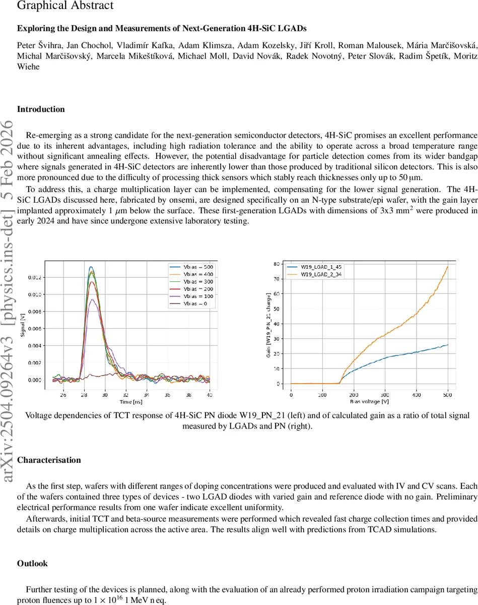
Transient Current Technique (TCT) measurements used 375 nm sub‑nanosecond laser pulses. The LGADs displayed a clear increase in transient current amplitude and integrated charge compared with the PN diode. Gain, defined as the charge ratio LGAD/PN, rose with bias and reached ≈20 for LGAD1 at 800 V. The pulse shapes indicate charge collection times on the order of tens of picoseconds, an essential prerequisite for precise timing.
Beta‑source measurements with a 90Sr source were performed on the same devices. By fitting the charge spectra with a Landau‑Gaussian convolution, the most probable value (MPV) for LGAD1 confirmed a gain of about 20 relative to the expected MIP charge (≈2 550 e⁻ for 50 µm SiC). The signal‑to‑noise ratio improved accordingly, and the timing resolution, extracted from coincidence measurements with reference silicon UFSDs, approached sub‑100 ps at 800 V bias. LGAD2, however, did not achieve the anticipated gain, suggesting that the higher dopant concentration may have introduced premature field‑clamping or gain‑suppression mechanisms that require further process optimisation.
Overall, the study demonstrates that 4H‑SiC LGADs can be fabricated with high yield, exhibit stable operation at high bias, provide moderate internal gain, and achieve timing performance comparable to silicon UFSDs while offering superior radiation tolerance and temperature stability. The authors plan further work that includes irradiation campaigns up to 1 × 10¹⁶ 1 MeV n_eq cm⁻², beam‑test campaigns, and refined TCAD simulations to optimise the gain‑layer profile and edge termination. The successful transfer of LGAD technology to a wide‑bandgap semiconductor opens the door to detectors for high‑luminosity colliders, space missions, and harsh‑environment medical applications.
Comments & Academic Discussion
Loading comments...
Leave a Comment