Tuning current flow in superconducting thin film strips by control wires. Applications to single photon detectors and diodes
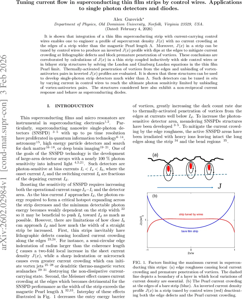
It is shown that integration of a thin film superconducting strip with current-carrying control wires enables one to engineer a profile of supercurrent density $J(x)$ with no current crowding at the edges of a strip wider than the magnetic Pearl length $Λ$. Moreover, $J(x)$ in a strip can be tuned by control wires to produce an inverted $J(x)$ profile with dips at the edges to mitigate current crowding at lithographic defects and block premature penetration of vortices. These conclusions are corroborated by calculations of $J(x)$ in a thin strip coupled inductively with side control wires or in bilayer strip structures by solving the London and Ginzburg Landau equations in the thin film Pearl limit. Thermally-activated penetration of vortices from the edges and unbinding of vortex-antivortex pairs in inverted $J(x)$ profiles are evaluated. It is shown that these structures can be used to develop single-photon strip detectors much wider than $Λ$. Such detectors can be tuned {\it in situ} by varying current in control wires to reach the ultimate photon sensitivity limited by unbinding of vortex-antivortex pairs. The structures considered here also exhibit a non-reciprocal current response and behave as superconducting diodes.
💡 Research Summary
The paper presents a novel method for engineering the current‑density profile J(x) in superconducting thin‑film strips by integrating adjacent current‑carrying control wires (or a second superconducting layer). In conventional superconducting nanowire single‑photon detectors (SNSPDs), when the strip width exceeds the Pearl length Λ, the Meissner screening forces the supercurrent to crowd at the edges. This edge crowding, amplified by lithographic defects or micro‑cracks, lowers the energy barrier for vortex entry, dramatically increasing dark‑count rates and limiting the usable bias current range.
The authors propose to place two control wires on either side of the strip, separated by a small gap b and raised a height h above the strip plane. By driving a dc current I₁ through these wires, a magnetic field is generated that opposes the self‑field of the strip near its edges. Solving the London equation in the Pearl limit (film thickness d ≪ λ) yields coupled integral equations for the gauge‑invariant potentials Q(x) in the strip and Q₁(x) in the wires. Numerical solutions for realistic material parameters (4 nm W₀.₈Si₀.₂ film with λ≈700 nm, Λ≈245 µm, and Nb control wires with λ≈50 nm) show that modest ratios I₁/I (as low as 0.6 for w≈4Λ) flatten the central J(x) and create pronounced dips at the edges. The dips can be deepened by increasing I₁, effectively suppressing the Pearl crowding for strips arbitrarily wider than Λ.
Two bilayer configurations are examined. When two identical layers carry opposite currents, their magnetic fields cancel, eliminating edge crowding entirely. When the layers are made of different superconductors (Λ₁ ≪ Λ), the lower‑Λ₁ layer acts as a tunable “under‑layer” that reshapes the J(x) of the upper detector layer in the same way as side wires, but with higher packing density for array implementations.
Beyond the linear London regime, the authors solve the Ginzburg‑Landau equations to capture the nonlinear current‑pair‑breaking behavior near the depairing current J_d. They find that in the inverted J(x) profile the maximum current density occurs in the strip interior, while the edges are deliberately weakened. Consequently, vortex entry from the edges is suppressed and the dominant dark‑count mechanism becomes thermally activated unbinding of vortex‑antivortex pairs in the bulk. By tuning I₁, the detector can be driven to the theoretical limit where the switching current I_b approaches I_d and the photon‑count efficiency is limited only by bulk pair unbinding.
A striking side effect is the emergence of a non‑reciprocal current‑voltage characteristic when the control‑wire current is reversed, turning the structure into a superconducting diode. This diode behavior arises from the asymmetric redistribution of supercurrent and could be exploited for low‑dissipation rectification.
Experimental relevance is highlighted by recent work (Ref. 38) where 3 nm‑thick, 0.1 mm‑wide WSi strips were integrated with Nb side rails, achieving 100 % infrared detection efficiency, a 20 % increase in switching current, and an eight‑order‑of‑magnitude reduction in dark counts. The theoretical framework presented here explains those results and predicts that even wider strips (several times Λ) can be used without sacrificing performance, provided the control currents are appropriately set.
In summary, the paper demonstrates that (1) current crowding in wide superconducting strips can be eliminated by inductively coupled control wires or bilayer under‑layers; (2) edge‑localized current dips can be engineered to neutralize lithographic defects; (3) the bias current range can be expanded up to the depairing limit, enabling ultimate photon‑sensitivity; (4) the same architecture yields a superconducting diode via non‑reciprocal response; and (5) the approach is scalable to large‑area detector arrays with minimal additional wiring. These insights open a pathway toward next‑generation, large‑area, ultra‑sensitive superconducting photon detectors and low‑loss superconducting electronic components.
Comments & Academic Discussion
Loading comments...
Leave a Comment