Depth Calibration of Double-sided Strip Germanium Detectors for the Compton Spectrometer and Imager Satellite
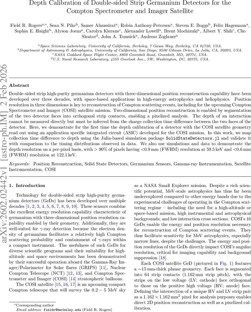
Double-sided strip high-purity germanium detectors with three-dimensional position reconstruction capability have been developed over three decades, with space-based applications in high-energy astrophysics and heliophysics. Position resolution in three dimensions is key to reconstruction of Compton scattering events, including for the upcoming Compton Spectrometer and Imager (COSI) satellite mission. Two-dimensional position reconstruction is enabled by segmentation of the two detector faces into orthogonal strip contacts, enabling a pixelized analysis. The depth of an interaction cannot be measured directly but must be inferred from the charge collection time difference between the two faces of the detector. Here, we demonstrate for the first time the depth calibration of a detector with the COSI satellite geometry read out using an application specific integrated circuit (ASIC) developed for the COSI mission. In this work, we map collection time difference to depth using the Julia-based simulation package SolidStateDetectors$.$jl and validate it with comparison to the timing distributions observed in data. We also use simulations and data to demonstrate the depth resolution on a per-pixel basis, with >90% of pixels having <0.9 mm (FWHM) resolution at 59.5 keV and <0.6 mm (FWHM) resolution at 122.1 keV.
💡 Research Summary
This paper presents the first depth‑calibration of a double‑sided strip high‑purity germanium detector (GeD) built to the geometry of the upcoming Compton Spectrometer and Imager (COSI) satellite, using the mission‑specific application‑specific integrated circuit (ASIC) readout. The detector (HP52301‑1) is a 15.2 mm thick planar crystal segmented into 64 orthogonal strips on each face, yielding 4096 pixels with a 1.162 mm pitch. Because the interaction depth (z) cannot be measured directly, it must be inferred from the charge‑collection time difference (τCTD) between the signals on the high‑voltage (HV) and low‑voltage (LV) faces. τCTD‑z mapping is highly non‑linear, depending on bias voltage, impurity concentration, temperature, and carrier mobility, and must be calibrated for each detector under its operating conditions.
The authors employ the Julia‑based simulation package SolidStateDetectors.jl to compute the electric field, weighting potentials, and charge‑cloud transport (including diffusion, Coulomb repulsion, and trapping). The ASIC chain provides a slow shaper (2 µs Gaussian) for energy and a fast shaper (60 ns Gaussian) for timing; when the fast shaper peaks, an analog voltage ramp is started and digitized as the TAC value. Per‑strip calibrations of energy and TAC are performed using injected test pulses.
Depth‑calibration data are acquired with 241 Am (59.5 keV) and 57 Co (122.1 keV) sources placed ~20 cm from the detector, illuminating either the HV or LV face. Because the sources are far enough that the photon flux follows an exponential attenuation law, the depth distribution in each pixel is approximately exponential with an effective attenuation depth λz (≈0.95 mm for 59.5 keV, ≈5.2 mm for 122.1 keV, as determined by Geant4). Low‑level cuts (energy thresholds, single‑pixel events, line‑energy windows, fast‑shaper thresholds) are applied to isolate clean single‑site photo‑peak events.
The measured τCTD histograms show distinct peaks for HV‑face illumination (τCTD ≈ +180 ns) and LV‑face illumination (τCTD ≈ –160 ns), reflecting the opposite drift directions of electrons and holes. The simulated τCTD‑z model, incorporating the non‑linear weighting potential near the contacts (small‑pixel effect), is fitted to the data for each pixel, yielding a per‑pixel τCTD‑z conversion function. The fit accounts for carrier mobility variations with temperature (≈83 K) and the high bias (1000 V).
Depth resolution is quantified as the full‑width at half‑maximum (FWHM) of the reconstructed z distribution for each pixel. At 59.5 keV, >90 % of the 4096 pixels achieve <0.9 mm (FWHM) resolution; at 122.1 keV, >90 % achieve <0.6 mm (FWHM). These values represent a substantial improvement over previous calibrations of similar detectors and meet the stringent requirements for COSI’s Compton event reconstruction, directly impacting the angular resolution measure (ARM) and background rejection capability.
The paper also discusses systematic effects inherent to the ASIC timing readout: charge‑trapping, inter‑strip charge sharing, capacitive cross‑talk, and electronic noise. The small‑pixel effect causes a steep τCTD‑z slope near the detector faces, which the simulation reproduces and the calibration corrects. The authors demonstrate that the Julia‑based framework can be readily adapted to other detector geometries and operating conditions, providing a powerful tool for future space‑borne germanium instruments.
In summary, the work delivers a complete workflow—from detailed physical modeling, through ASIC‑specific timing calibration, to pixel‑by‑pixel depth reconstruction—that validates the COSI detector design and ensures that the satellite will achieve the required three‑dimensional position resolution for high‑fidelity MeV γ‑ray imaging.
Comments & Academic Discussion
Loading comments...
Leave a Comment