Fabrication effects on Niobium oxidation and surface contamination in Niobium-metal bilayers using X-ray photoelectron spectroscopy
Superconducting resonators and qubits are limited by dielectric losses from surface oxides. Surface oxides are mitigated through various strategies such as the addition of a metal capping layer, surface passivation, and acid processing. In this study, we demonstrate the use of X-ray photoelectron spectroscopy (XPS) as a rapid characterization tool to study the effectiveness cap layers for niobium for further device fabrication. We non-destructively evaluate 17 capping layers to characterize their ability to prevent oxygen diffusion, and the effects of standard fabrication processes – annealing, resist stripping, and acid cleaning. We downselect for resilient capping layers and test their microwave resonator performance.
💡 Research Summary
This paper investigates how different metal, nitride, and alloy capping layers affect the oxidation of niobium (Nb) surfaces and the resulting dielectric losses in superconducting quantum devices. Using X‑ray photoelectron spectroscopy (XPS) as a rapid, non‑destructive probe, the authors evaluate 17 candidate capping materials for their ability to block oxygen diffusion and resist contamination during typical fabrication steps: annealing, resist stripping, and acid cleaning.
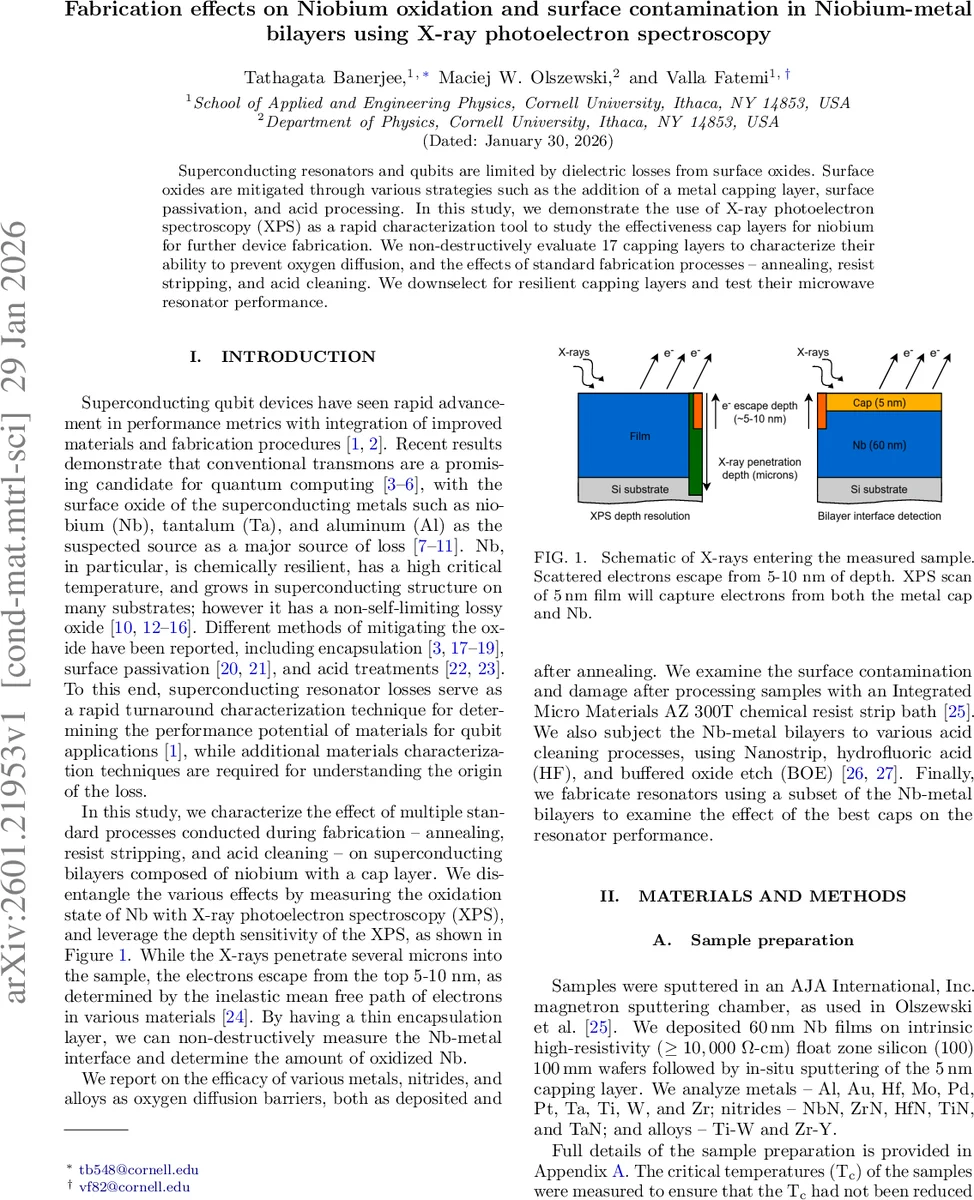
The experimental workflow begins with sputtering 60 nm Nb films on high‑resistivity silicon, followed by an in‑situ deposition of a 5 nm capping layer. The capping set includes ten pure metals (Al, Au, Hf, Mo, Pd, Pt, Ta, Ti, W, Zr), five nitrides (NbN, ZrN, HfN, TiN, TaN), and two alloys (Ti‑W, Zr‑Y). XPS measurements, which sample the top 5–10 nm of material, are performed on unprocessed samples and after each processing step. By fitting the Nb 3d core‑level spectra, the authors quantify the fractions of metallic Nb, sub‑oxides (NbO, NbO₂) and fully oxidized Nb₂O₅, while also detecting surface contaminants such as carbon, nitrogen, sodium, calcium, and silicon.
Annealing results: Heating at 200 °C for one hour in air or vacuum reveals that Al, Hf, Mo, Ta, Ti, W, Zr, and the two alloys effectively prevent Nb oxidation, showing negligible Nb₂O₅ peaks. In contrast, noble metals Au, Pd, and Pt allow significant oxygen diffusion, especially when the capping film is thin, leading to pronounced Nb₂O₅ signals. Among nitrides, TiN and ZrN show modest oxidation, whereas NbN’s spectrum is ambiguous due to overlapping NbNₓ and NbO peaks, making its barrier performance uncertain.
Resist‑strip (AZ 300T) results: The chemical stripper (NMP‑based with TMAH) introduces surface contaminants (C, N, Na, Ca, Si). Mo, W, and Ti‑W caps are etched away, exposing Nb that subsequently oxidizes, rendering these caps unsuitable for processes involving heated strippers. Au, Pd, Zr, and Zr‑Y retain the cleanest surfaces with the lowest contaminant levels, indicating good compatibility with standard lithography steps.
Acid‑cleaning results: The authors test three aggressive treatments—2 % HF, 10:1 buffered oxide etch (BOE), and a 30‑minute Nanostrip soak. Ta and TaN survive all three without visible degradation, making them the most chemically robust. TiN and Mo survive HF and BOE but are etched by Nanostrip, exposing Nb. Hf, Ti, Zr, HfN, and Zr‑Y are completely damaged by each acid, likely due to their high reactivity.
Resonator performance: Based on the XPS screening, four caps (Ta, Zr, TaN, TiN) are selected for fabricating λ/4 coplanar waveguide resonators (target 4–8 GHz) on the same Nb platform. Measurements at 500 mK reveal that Ta‑ and TaN‑capped resonators exhibit a markedly lower medium‑power loss (δ_MP) compared to uncapped Nb, directly linking reduced Nb surface oxide to improved quality factors. TiN‑capped devices show δ_MP comparable to bare Nb but achieve a lower high‑power loss (δ_HP), suggesting that TiN’s own oxide contributes less to loss at high photon numbers but may host a higher density of two‑level systems (TLS) at low power. Zr‑capped resonators perform worse than the control, consistent with the fact that the Zr layer itself fully oxidizes, adding an extra lossy dielectric layer. Post‑fabrication XPS confirms that surface contamination levels are similar across all devices, indicating that the observed loss differences stem primarily from the intrinsic properties (thickness, loss tangent, dielectric constant) of the respective cap oxides.
Conclusions and outlook: The study demonstrates that XPS can serve as an efficient screening tool for selecting capping materials that both block oxygen diffusion and survive standard microfabrication chemicals. Ta and TaN emerge as the most promising candidates, offering chemical resilience and clear loss reduction in superconducting resonators. The work also highlights that a capping layer’s own oxidation behavior critically influences device performance; a thick, high‑loss oxide (as with Zr) can negate the benefits of oxygen blocking. Future investigations should explore thickness optimization, long‑term thermal stability, and direct TLS spectroscopy on capped devices to fully characterize the microscopic loss mechanisms introduced by each cap material.
Comments & Academic Discussion
Loading comments...
Leave a Comment