Near-field effects on cathodoluminescence outcoupling in perovskite thin films
Halide perovskite semiconductors are a promising material for high-efficiency solar cells. Their optical properties can vary within and between crystallographic grains. We present spatially-resolved cathodoluminescence (CL) spectroscopy at 2 keV and 5 keV on polycrystalline CsPbBr3 perovskite films to study these variations at the nanoscale. The CL maps show a strongly reduced intensity near the polycrystalline grain boundaries. We perform numerical simulations of the far-field emission of the electron beam-generated optical near fields using the surface profiles from AFM as input. We find that near grain boundaries the light outcoupling is strongly reduced due to enhanced internal reflection and light trapping at the curved surfaces. Lateral variations in CL intensity inside grains are due to Fabry-Perot-like resonances in the film, with the substrate acting as a back reflector. Our results show that near-field coupling and interference effects can dominate nanoscale luminescence maps of halide perovskite films. The results are broadly relevant for the analysis of cathodoluminescence and photoluminescence of corrugated thin films.
💡 Research Summary
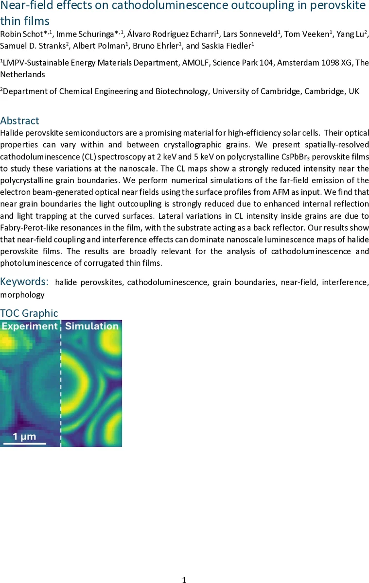
This paper investigates how the micro‑ and nano‑scale morphology of polycrystalline CsPbBr₃ perovskite thin films influences the spatial distribution of cathodoluminescence (CL) emission. Using a scanning electron microscope equipped for CL spectroscopy, the authors acquire high‑resolution CL maps at two electron beam energies, 2 keV and 5 keV, which correspond to shallow (≈30 nm) and deeper (≈150 nm) excitation volumes, respectively. Simultaneously, atomic force microscopy (AFM) provides topographical maps of the same regions, revealing grain sizes ranging from ~100 nm to several micrometers and surface height variations up to 120 nm, with pronounced valleys at grain boundaries.
Monte‑Carlo simulations of electron trajectories quantify the spatial distribution of deposited energy for each beam energy, confirming that the 2 keV beam probes only the near‑surface region while the 5 keV beam samples a much larger volume. To translate these energy deposition profiles into optical emission, the authors perform finite‑difference time‑domain (FDTD) simulations. They place an ensemble of incoherent electric dipoles (representing radiative recombination) throughout the film, conforming to the measured AFM surface profile, and weight each dipole’s contribution by the local energy density obtained from the Monte‑Carlo results. The far‑field radiation from each dipole is summed over all orientations and integrated over the upper hemisphere, yielding a simulated CL intensity map that can be directly compared with experiment.
The simulations reproduce two key experimental observations. First, CL intensity drops sharply at grain boundaries. The curved surface topography at these boundaries enhances internal reflection of the near‑field components, effectively trapping light within the perovskite layer and reducing the amount that escapes into the detector. This optical out‑coupling loss explains the “dark lines” seen in the CL maps without invoking increased non‑radiative recombination. Second, within large grains the CL maps display concentric rings of alternating bright and dark intensity. These rings arise from Fabry‑Perot‑like interference between light reflected at the film‑air interface and at the silicon substrate beneath the perovskite. The interference period (~100 nm) matches the optical path length for 525 nm emission in CsPbBr₃ (n≈2.67). Because the 2 keV excitation is confined near the surface, the CL signal is highly sensitive to the exact position of constructive or destructive interference, producing pronounced rings. The deeper 5 keV excitation averages over multiple interference maxima and minima, diminishing the ring contrast, as observed experimentally.
Further analysis extends the model into three dimensions by simulating sheets of dipoles at various depths (10–50 nm) that follow the actual surface contour of a grain. The simulated concentric patterns shift inward with increasing dipole depth, consistent with the interference model for a convex grain surface. Overlaying the 30 nm‑depth simulation onto the experimental 2 keV CL map yields excellent agreement, confirming that the majority of the 2 keV CL originates from a depth of ~20–30 nm.
Overall, the study demonstrates that nanoscale surface morphology can dominate CL intensity variations through near‑field coupling and thin‑film interference, challenging the common attribution of grain‑boundary CL quenching solely to non‑radiative recombination. The combined Monte‑Carlo/FDTD framework provides a quantitative tool for interpreting CL (and by extension photoluminescence) maps of corrugated semiconductor films. These insights are broadly relevant for the design and optical characterization of perovskite optoelectronic devices, where controlling surface topography and film thickness can be leveraged to optimize light out‑coupling and overall device performance.
Comments & Academic Discussion
Loading comments...
Leave a Comment