Experimental Demonstration of Nonlinear Photoconductive Gain in N-Doped $β$-Ga$_2$O$_3$ Devices
Photoconductive devices based on ultra-wide-bandgap (UWBG) materials offer a promising pathway toward compact, high-voltage (HV) optoelectronic and optical sensing in harsh environments. In this Letter, we report field-tunable nonlinear photoconductive gain in vertical $β$-Ga$_2$O$_3$ photoconductive devices under sub-bandgap visible-light excitation. The devices were fabricated on a $5.6,μ\text{m}$-thick nitrogen-doped semi-insulating $β$-Ga$_2$O$_3$ epilayer grown on a conductive Sn-doped substrate and characterized under $445,\text{nm}$ continuous-wave illumination. A distinct transition from linear to nonlinear photoconductive behavior is observed at a threshold electric field of approximately $0.67,\text{MV/cm}$, resulting in an approximately $20\times$ enhancement in photocurrent. Complementary TCAD simulations indicate strong electric-field localization and a rapid increase in impact-ionization generation at high bias, suggesting that impact-ionization–assisted carrier multiplication contributes to the observed gain. These results demonstrate a high-field visible-light photoconductive detection mode in $β$-Ga$_2$O$_3$ enabled by defect-assisted transport, providing a pathway toward field-tunable gain photodetectors operating without deep-ultraviolet (DUV) excitation.
💡 Research Summary
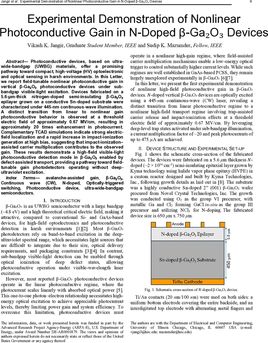
This paper presents the first experimental demonstration of nonlinear photoconductive gain in nitrogen‑doped vertical β‑Ga₂O₃ devices under continuous‑wave (CW) visible‑light excitation. The authors fabricated a 5.6 µm‑thick N‑doped semi‑insulating β‑Ga₂O₃ epilayer on a highly conductive Sn‑doped substrate, creating a vertical structure with Ti/Au top interdigitated contacts and a full‑area bottom electrode. The devices were immersed in Fluorinert to suppress surface flashover and were characterized at room temperature using a 3 W, 445 nm CW laser (core 105 µm, NA 0.22) and a Keithley 2657A high‑voltage SMU.
Electrical measurements reveal that dark current remains below the µA level up to ~300 V, after which it rises gradually. Under illumination, the photocurrent initially follows a linear dependence on bias, characteristic of the conventional photoconductive regime. At an electric field of approximately 0.67 MV/cm (≈ 325 V), a distinct transition to a nonlinear high‑gain regime occurs. Photocurrent then increases sharply, reaching peak values of ~475 µA (device 1) and ~450 µA (device 2) at 435–445 V, representing a 20‑23‑fold enhancement relative to the linear regime.
Transient measurements show a modest, slowly varying response at 300 V, while at 400 V and 425 V a pronounced peak followed by a slower decay appears. The bias‑dependent peak amplitude and steady‑state level indicate that carrier generation is strongly amplified at high fields, with trap‑assisted release contributing to the initial surge and subsequent trapping governing the decay.
To elucidate the underlying physics, the authors performed 2‑D drift‑diffusion TCAD simulations (Silvaco ATLAS) incorporating the measured material parameters: background donor concentration ND = 1.6 × 10¹⁵ cm⁻³, a deep nitrogen acceptor trap (Nt = 1.9 × 10¹⁶ cm⁻³, EC = ‑2.9 eV, capture cross‑sections σn = σp = 2 × 10⁻¹⁶ cm²), field‑dependent mobility, SRH recombination, Auger processes, and the Selberherr impact‑ionization model (An = Ap = 2.5 × 10⁶ cm⁻¹, Bn = Bp = 3.96 × 10⁷ V·cm⁻¹). Simulated electric‑field profiles show monotonic increase with bias, reaching >1.5 MV/cm near the contacts at 400–425 V. Correspondingly, the impact‑ionization generation rate spikes by several orders of magnitude, attaining 10¹⁶–10¹⁸ cm⁻³·s⁻¹, localized primarily at the high‑field regions. This localized avalanche‑like multiplication provides an additional carrier source that, together with bulk trap‑assisted transport, accounts for the observed high‑gain behavior.
The work demonstrates that β‑Ga₂O₃, traditionally employed for deep‑UV photodetection, can be activated by sub‑bandgap visible photons through deep‑level optical ionization. By leveraging a thin N‑doped insulating layer on a conductive substrate, high electric fields are achieved at relatively modest voltages, enabling a field‑tunable gain mechanism without the need for DUV light sources. The reported 20‑fold photocurrent enhancement and peak currents approaching 0.5 mA illustrate the potential for compact, high‑voltage photoconductive switches, optical sensors, and gain‑controlled photodetectors operating in harsh environments.
Future directions include engineering trap densities and energy levels to optimize gain, refining electrode geometries to control field localization, and extending the study to pulsed excitation for high‑speed applications. The combination of defect‑assisted transport and impact‑ionization in an ultra‑wide‑bandgap material opens a new pathway for high‑performance, field‑tunable optoelectronic devices that can operate under visible illumination while maintaining the robustness required for power‑electronics and space‑qualified systems.
Comments & Academic Discussion
Loading comments...
Leave a Comment