Experimental Demonstration of Nonlinear Photoconductive Gain in N-Doped $β$-Ga$_2$O$_3$ Devices
Photoconductive devices based on ultra-wide-bandgap (UWBG) materials offer a promising pathway toward compact, high-voltage (HV) optoelectronic and optical sensing in harsh environments. In this Letter, we report field-tunable nonlinear photoconductive gain in vertical $β$-Ga$_2$O$_3$ photoconductive devices under sub-bandgap visible-light excitation. The devices were fabricated on a $5.6,μ\text{m}$-thick nitrogen-doped semi-insulating $β$-Ga$_2$O$_3$ epilayer grown on a conductive Sn-doped substrate and characterized under $445,\text{nm}$ continuous-wave illumination. A distinct transition from linear to nonlinear photoconductive behavior is observed at a threshold electric field of approximately $0.67,\text{MV/cm}$, resulting in an approximately $20\times$ enhancement in photocurrent. Complementary TCAD simulations indicate strong electric-field localization and a rapid increase in impact-ionization generation at high bias, suggesting that impact-ionization–assisted carrier multiplication contributes to the observed gain. These results demonstrate a high-field visible-light photoconductive detection mode in $β$-Ga$_2$O$_3$ enabled by defect-assisted transport, providing a pathway toward field-tunable gain photodetectors operating without deep-ultraviolet (DUV) excitation.
💡 Research Summary
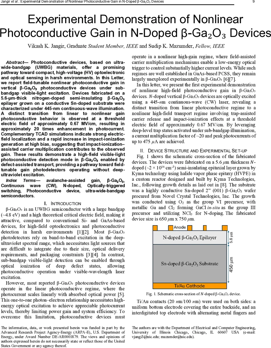
This paper reports the first experimental demonstration of nonlinear photoconductive gain in nitrogen‑doped β‑Ga₂O₃ vertical devices under continuous‑wave (CW) visible‑light excitation. The authors grew a 5.6 µm‑thick semi‑insulating β‑Ga₂O₃ epilayer doped with nitrogen (≈2 × 10¹⁶ cm⁻³) on a highly conductive Sn‑doped β‑Ga₂O₃ substrate using halide vapor phase epitaxy. Ti/Au contacts were patterned on both sides, forming a uniform bottom electrode and an interdigitated top electrode to ensure a homogeneous electric field while allowing optical access. Devices were immersed in Fluorinert during testing to suppress surface flashover at high bias.
Electrical characterization was performed with a Keithley 2657A source‑measure unit while the devices were illuminated by a 3 W, 445 nm CW diode laser (core = 105 µm, NA = 0.22). In the dark, the current remained below 1 µA up to ~300 V, after which a modest increase was observed. Under illumination, the photocurrent initially rose linearly with bias, reflecting the conventional photoconductive regime. However, at a threshold electric field of approximately 0.67 MV/cm (corresponding to 325–350 V across the 5.6 µm layer), a distinct transition to a nonlinear regime occurred. Photocurrent surged by roughly 20‑fold, reaching peak values of 475 µA (device 1 at 435 V) and 450 µA (device 2 at 445 V). Temporal measurements showed that at higher bias the response featured a sharp transient peak followed by a slower decay, indicating trap‑mediated carrier dynamics combined with rapid carrier generation.
To elucidate the underlying physics, the authors performed 2‑D TCAD simulations in Silvaco ATLAS. The model incorporated the measured nitrogen acceptor trap (Nₜ = 1.9 × 10¹⁶ cm⁻³, Eₜ = −2.9 eV, capture cross‑sections σₙ = σₚ = 2 × 10⁻¹⁶ cm²) and background Si donors (N_D = 1.6 × 10¹⁵ cm⁻³). The conductive substrate was represented with N_D ≈ 5 × 10¹⁹ cm⁻³ to provide low‑resistance spreading. Field‑dependent mobility, SRH recombination, Auger processes, and the Selber‑Herr impact‑ionization model (Aₙ = Aₚ = 2.5 × 10⁶ cm⁻¹, Bₙ = Bₚ = 3.96 × 10⁷ V·cm⁻¹) were included. Simulations showed that the electric field increases monotonically with bias and exceeds 1.5 MV/cm near the contacts at 400 V and above. Correspondingly, the impact‑ionization generation rate spikes by several orders of magnitude, reaching 10¹⁶–10¹⁸ cm⁻³·s⁻¹. Although the high‑field region is localized, the resulting carrier multiplication provides an additional current path that amplifies the overall photocurrent.
The authors conclude that the observed high‑gain behavior originates from a synergistic combination of trap‑assisted carrier release and impact‑ionization‑driven avalanche multiplication. The nitrogen‑related deep traps enable sub‑bandgap photon absorption, while the vertical device geometry and conductive substrate concentrate the electric field, allowing avalanche processes to activate at relatively modest voltages (≈ 400 V). This mechanism yields a ~20× gain without requiring deep‑UV illumination, opening a pathway toward compact, high‑field photoconductive detectors and switches that can be triggered by inexpensive visible‑laser sources.
Key implications include: (1) Demonstration that β‑Ga₂O₃, traditionally a DUV photodetector material, can operate efficiently under visible excitation when engineered with deep traps and high electric fields; (2) Validation that impact‑ionization in β‑Ga₂O₃ can provide substantial gain, similar to GaAs‑based photoconductive semiconductor switches but at much higher breakdown fields, offering higher voltage and power handling capability; (3) Potential for integrating such devices into high‑voltage pulsed power systems, optical‑triggered switches, and harsh‑environment sensors where DUV sources are impractical. Future work is suggested to optimize trap density, electrode design, and thermal management to further enhance gain, speed, and reliability for real‑world applications.
Comments & Academic Discussion
Loading comments...
Leave a Comment