Conveyor-mode electron shuttling through a T-junction in Si/SiGe
Conveyor-mode shuttling in gated Si/SiGe devices enables adiabatic transfer of single electrons, electron patterns and spin qubits confined in quantum dots across several microns with a scalable number of signal lines. To realize their full potential, linear shuttle lanes must connect into a two-dimensional grid with controllable routing. We introduce a T-junction device linking two independently driven shuttle lanes. Electron routing across the junction requires no extra control lines beyond the four channels per conveyor belt. We measure an inter-lane charge transfer fidelity of $F = 100.0000000^{+0}_{-9\times 10^{-7}},%$ at an instantaneous electron velocity of $270,\mathrm{mm},\mathrm{s}^{-1}$. The filling of 54 quantum dots is controlled by simple atomic pulses, allowing us to swap electron patterns, laying the groundwork for a native spin-qubit SWAP gate. This T-junction establishes a path towards scalable, two-dimensional quantum computing architectures with flexible spin qubit routing for quantum error correction.
💡 Research Summary
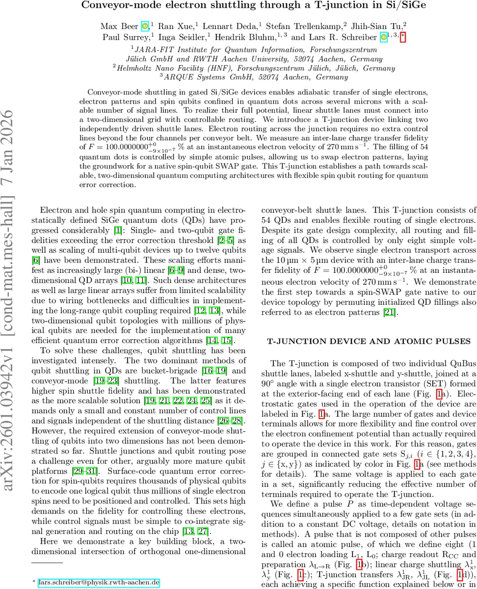
In this work the authors demonstrate a two‑dimensional electron‑shuttling architecture based on a T‑junction that links two independently driven conveyor‑mode shuttle lanes fabricated in a Si/SiGe heterostructure. The device comprises 54 electrostatically defined quantum dots (QDs) arranged in two orthogonal linear arrays (the “x‑shuttle” and the “y‑shuttle”) that intersect at a right angle. By grouping the metallic gates into four gate‑sets per lane and applying the same voltage to all gates within a set, the authors reduce the number of required control lines to just eight “atomic” voltage pulses (plus a few static bias lines). These eight pulses—electron loading (L₁, L₀), charge readout (R_CC), linear shuttling in each lane (λ₁ˣ, λ₁ʸ), and two junction‑transfer pulses (λ₁ᴶᴿ, λ₁ᴶᴸ)—are sufficient to initialise, move, and read out any configuration of electrons across the whole structure.
The conveyor‑mode shuttling is realised with sinusoidal gate‑voltage waveforms ΔV_g = A sin(2πt/T_λ + i·π/2), where i ∈ {1,2,3,4} indexes the four gates that define a single quantum dot. One period T_λ moves an electron by λ ≈ 280 nm, giving an instantaneous velocity v_λ ≈ 270 mm s⁻¹ for the parameters used (A ≈ 260 mV). The junction‑transfer pulses synchronise the x‑ and y‑shuttle drives (amplitude A_J, velocity v_J) and pause each lane at T_λ/4 intervals so that an electron can be handed over from QD_X₁₇ to QD_Y₀ (λ₁ᴶᴿ) or from QD_X₁₈ to QD_Y₀ (λ₁ᴶᴸ) without encountering a potential barrier.
Single‑electron shuttling experiments first verify that an electron loaded into QD_X₀ can be moved forward along the x‑shuttle, turned at the junction, and then propagated along the y‑shuttle, finally returning to its original location. Success is defined by detecting the electron only at the expected readout position (Δn = 0) and never elsewhere. Over 1 000 repetitions the inter‑lane transfer fidelity is measured as F = 100.0000000 % ± 9 × 10⁻⁷ % (the error bar is limited by the read‑out and loading steps rather than the shuttling itself). No spurious electrons are observed when the device is deliberately loaded with zero electrons, confirming a negligible background error rate.
To probe the intrinsic reliability of the junction transfer, the authors devise a looping protocol. After moving an electron to the centre of the T‑junction, they repeatedly apply a junction‑transfer pulse followed by 25 periods of linear shuttling in the opposite lane, effectively moving the electron back and forth across the junction. By varying the number of loops (n = 10⁴, 10⁵, 10⁶) they extract a per‑loop fidelity F₁ that remains at 100.0000000 % ± 9 × 10⁻⁷ % for drive amplitudes A_J ≥ 133 mV and velocities from 28 mm s⁻¹ up to 270 mm s⁻¹. Even when the drive amplitude is reduced to the minimal reliable value of 100 mV, the fidelity does not degrade, indicating that the junction transfer is intrinsically error‑free within the experimental resolution.
Beyond single‑electron transport, the authors demonstrate the simultaneous preparation of arbitrary electron patterns (multiple occupied dots) in both shuttles. By loading a pattern into the right half of the x‑shuttle, shuttling it into the y‑shuttle via λ₁ᴶᴿ, and then loading a new pattern into the full x‑shuttle, they achieve a deterministic swap of the two patterns. This capability is a concrete step toward a native spin‑SWAP gate, which is a key primitive for quantum error‑correction codes that require flexible routing of qubits across a two‑dimensional lattice.
The paper’s key technical insights are: (1) a minimal set of eight control pulses can fully manipulate a 54‑dot two‑dimensional array, dramatically reducing wiring complexity; (2) the conveyor‑mode shuttling retains its high spin‑preserving fidelity when extended to a 2‑D junction, with error rates below 10⁻⁶ even at high velocities; (3) statistical analysis of millions of loop cycles confirms that the dominant error sources lie in loading and read‑out, not in the shuttling dynamics themselves; and (4) the demonstrated pattern‑swap operation provides a hardware‑level pathway to implement SWAP‑based routing and entanglement distribution in large‑scale spin‑qubit processors.
Overall, this work establishes that conveyor‑mode electron shuttling can be scaled from one‑dimensional lines to a two‑dimensional grid without sacrificing fidelity or speed, thereby addressing a major bottleneck in the roadmap toward million‑qubit silicon quantum processors. The T‑junction architecture, combined with the atomic‑pulse control scheme, offers a practical blueprint for constructing flexible, low‑overhead routing networks essential for fault‑tolerant quantum computing.
Comments & Academic Discussion
Loading comments...
Leave a Comment