3D Printing as a Rapid Prototyping Approach for Novel RF Cavity Designs
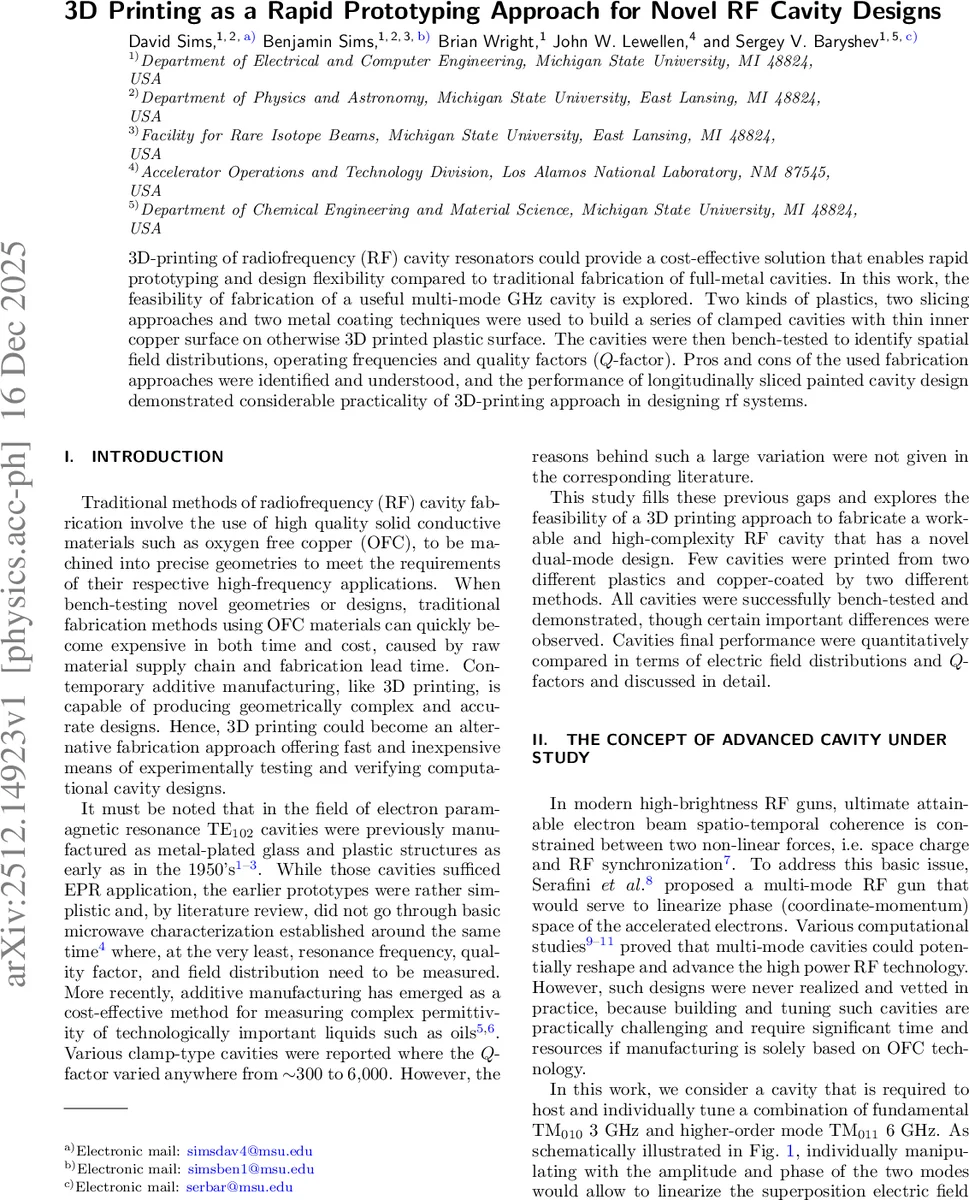
3D-printing of radiofrequency (RF) cavity resonators could provide a cost-effective solution that enables rapid prototyping and design flexibility compared to traditional fabrication of full-metal cavities. In this work, the feasibility of fabrication of a useful multi-mode GHz cavity is explored. Two kinds of plastics, two slicing approaches and two metal coating techniques were used to build a series of clamped cavities with thin inner copper surface on otherwise 3D printed plastic surface. The cavities were then bench-tested to identify spatial field distributions, operating frequencies and quality factors (Q-factor). Pros and cons of the used fabrication approaches were identified and understood, and the performance of longitudinally sliced painted cavity design demonstrated considerable practicality of 3D-printing approach in designing rf systems.
💡 Research Summary
This paper investigates the feasibility of using additive manufacturing—specifically desktop stereolithography 3‑D printing—to fabricate radio‑frequency (RF) cavity resonators that support two distinct modes, the fundamental TM₀₁₀ at 3 GHz and the higher‑order TM₀₁₁ at 6 GHz. The authors designed a dual‑mode cavity in COMSOL, incorporating ports for couplers and tuners, and then printed the structure in two halves using a Stratasys J55 Prime printer with a photopolymer resin (VeroUltraWhite). To create the conductive interior required for RF operation, they explored two coating techniques: (i) physical vapor deposition (sputtering) of a 30 nm titanium adhesion layer followed by 5 µm of copper, and (ii) application of a water‑based silver conductive paint in three successive coats.
A key variable was the slicing orientation used to split the cavity for printing. Two strategies were examined: longitudinal (along the beam axis) and latitudinal (perpendicular to the beam axis). The slicing direction determines where the printed layers intersect the surface‑current paths that dominate RF losses. The authors hypothesized that interruptions aligned with the magnetic‑field‑driven current would increase loss, while interruptions aligned with the electric field would have a lesser effect.
Four cavities were fabricated: (1) longitudinally sliced and sputter‑coated, (2) longitudinally sliced and paint‑coated, (3) latitudinally sliced and sputter‑coated (failed due to shadowing of the nose‑cone geometry), and (4) latitudinally sliced and paint‑coated. The failed sputter case highlighted a practical limitation: complex internal geometries can block line‑of‑sight for the sputtering source, leading to uneven metal deposition.
The cavities were characterized using a “wire‑pull” technique to map the axial electric‑field distribution of both TM₀₁₀ and TM₀₁₁ modes, confirming that the dual‑mode behavior was achieved. Vector network analyzer (VNA) measurements of S₁₁ and S₂₁ were performed after careful impedance matching on a Smith chart to achieve critical coupling (β≈1). Loaded Q (Q_L) was extracted from the –3 dB bandwidth, and intrinsic Q (Q₀) was calculated as Q₀=(1+β)Q_L.
Results (summarized in Table I) show a clear dependence on both slicing and coating. The latitudinally sliced, paint‑coated cavity achieved Q₀≈1 364 for TM₀₁₀ and Q₀≈1 423 for TM₀₁₁, roughly four times higher than its longitudinal counterpart (Q₀≈320/336). The longitudinally sliced, sputter‑coated cavity performed better than the paint version (Q₀≈623/698) but still lagged behind the latitudinal design. The authors infer that a latitudinally sliced cavity with a uniform sputtered copper coating would likely deliver the highest Q, though this configuration could not be experimentally verified due to the shadowing issue.
The discussion links these observations to electromagnetic theory. Surface currents flow within the skin depth (≈1 µm at 3–6 GHz); any geometric discontinuity forces current crowding, raising the surface resistance and thus RF loss. Longitudinal slicing cuts across the dominant azimuthal current loops, increasing inductive loss, while latitudinal slicing mainly perturbs the electric‑field distribution, manifesting as a capacitive signature on the Smith chart. Consequently, the Smith‑chart quadrants provide a rapid diagnostic for mode identification and coupling quality.
Material considerations are also emphasized. Sputtered copper films, being dense and smooth, approximate bulk conductivity and require only a few skin depths to be effective. In contrast, silver‑based conductive paints are porous and rough, leading to higher surface resistance and potential RF leakage. The authors note that coating thickness must exceed the skin depth to avoid penetration losses, and that manual painting makes achieving uniform thickness difficult.
In conclusion, the study demonstrates that 3‑D‑printed RF cavities are a viable, low‑cost platform for rapid prototyping of complex, multi‑mode resonators. Critical lessons include: (1) careful selection of slicing orientation to preserve uninterrupted surface‑current paths, (2) preference for metal deposition methods that ensure uniform, sufficiently thick conductive layers, and (3) awareness of geometric shadowing that can impede sputtering. Future work should explore alternative deposition techniques such as electroplating or electroless plating, and extend the approach to higher frequencies where skin depth is even smaller, thereby pushing the performance envelope of additive‑manufactured RF components.
Comments & Academic Discussion
Loading comments...
Leave a Comment