L2 Ethernet Switch VLSI Implementation
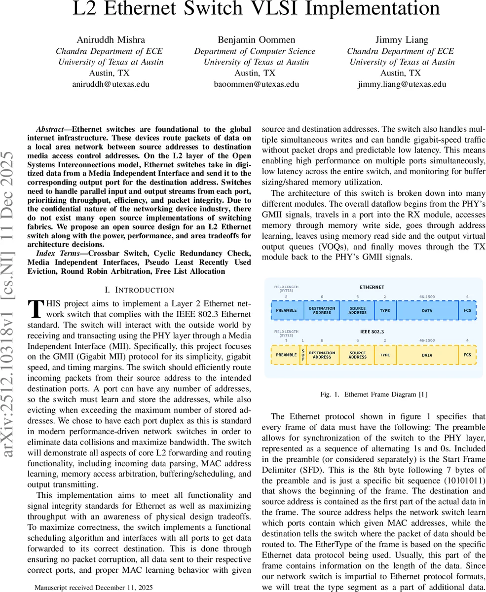
Ethernet switches are foundational to the global internet infrastructure. These devices route packets of data on a local area network between source addresses to destination media access control addresses. On the L2 layer of the Open Systems Interconnections model, Ethernet switches take in digitized data from a Media Independent Interface and send it to the corresponding output port for the destination address. Switches need to handle parallel input and output streams from each port, prioritizing throughput, efficiency, and packet integrity. Due to the confidential nature of the networking device industry, there do not exist many open source implementations of switching fabrics. We propose an open source design for an L2 Ethernet switch along with the power, performance, and area tradeoffs for architecture decisions.
💡 Research Summary
**
The paper presents an open‑source design and VLSI‑level implementation of a four‑port Layer‑2 Ethernet switch that complies with the IEEE 802.3 standard. The authors focus on the Gigabit Media Independent Interface (GMII) as the external interface because it offers a simple parallel 8‑bit, 125 MHz connection that comfortably supports 1 Gbps line rate while providing generous timing margins for silicon verification.
The overall data path starts with GMII RX signals, passes through an asynchronous FIFO that bridges the 125 MHz GMII clock domain to the internal 500 MHz switch clock domain, and then enters the RX parsing module. The RX module detects the preamble (seven 0x55 bytes) and the Start‑of‑Frame delimiter (0xD5), extracts the destination and source MAC addresses, and continuously updates a CRC‑32 accumulator. When the GMII data‑valid signal de‑asserts, the module checks the calculated CRC against the received Frame Check Sequence (FCS). If a mismatch is found, an error flag and an end‑of‑frame (EOF) marker are written to memory, causing the frame to be dropped before it reaches the TX side.
Memory is organized as a centralized SRAM consisting of 64 registers, each 64 bytes wide, for a total of 4 KB. Each register stores 63 bytes of payload and a 1‑byte footer that contains a 6‑bit “next‑block” pointer and a 1‑bit end‑of‑packet (EOP) flag. This linked‑list style organization allows a frame to occupy non‑contiguous blocks while still being read sequentially. Allocation of SRAM blocks is managed by a free‑list implemented as a stack; allocating a block pops an index, freeing a block pushes the index back. To support the “flood” case—when a destination MAC is unknown—the design keeps a per‑block reference counter so that a block is returned to the free list only after the last egress port has finished transmitting the frame.
The memory write controller receives one byte per GMII clock from the RX module. It coalesces bytes into 63‑byte payload chunks, writes the payload to the currently allocated SRAM block, and, when the payload is complete or an EOF is signaled, writes the footer and requests a write port grant. Because the SRAM has a single write port, the authors evaluated two alternatives: multiple write ports (which would increase area and power) versus a round‑robin arbiter that serializes access from the four ingress ports. They chose the latter, noting that the arbiter introduces at most one cycle of latency per port and keeps the SRAM footprint minimal. When the free list cannot supply a block immediately, the write controller enters a WAIT state and de‑asserts its ready signal to the RX module, creating back‑pressure. The authors report that such stalls occur in less than 3 % of cycles in their simulations.
On the egress side, each port has its own memory read controller. The read controller follows the virtual output queue (V‑OQ) pointer stored in the SRAM footer, reads the linked blocks sequentially, and streams the data to the TX module. The TX module re‑generates the GMII TX signals (clock, data, enable, error) and transmits the frame to the PHY. The read side also uses a single SRAM read port, arbitrated by the same round‑robin scheme, ensuring fair access among ports. After a frame has been transmitted, the read controller decrements the reference counter for each block; when the counter reaches zero, the block is pushed back onto the free list.
The authors provide SystemVerilog source code on a public GitHub repository and validate functionality through simulation. They discuss several design trade‑offs:
- Area vs. Performance: A single‑port SRAM with round‑robin arbitration reduces silicon area and static power but introduces modest contention under heavy traffic.
- Memory Management: The free‑list stack and reference‑count scheme enable simultaneous allocations and frees without complex address translation logic.
- Error Handling: CRC‑based frame dropping is performed early, preventing corrupted data from propagating downstream.
- Flooding Mechanism: When the MAC address table misses, the switch floods the frame to all ports, a simple but bandwidth‑inefficient approach suitable for initial learning phases.
While the paper thoroughly describes the architecture, modules, and control flow, it lacks quantitative silicon results such as post‑layout area, dynamic power consumption, maximum operating frequency, and timing closure margins. The design is demonstrated only for a four‑port, 4 KB memory configuration, leaving open questions about scalability to larger port counts or higher‑speed interfaces (e.g., 10 GbE, SGMII). Moreover, the impact of the round‑robin arbiter on worst‑case latency under bursty traffic is not analyzed, nor are alternative arbitration schemes (e.g., priority‑based or weighted‑fair) explored.
In conclusion, the paper delivers a complete, open‑source reference implementation of a Layer‑2 Ethernet switch that balances simplicity, resource efficiency, and functional correctness. It serves as a valuable foundation for academic study and for developers seeking a baseline VLSI Ethernet switch design. Future work could extend the architecture to support more ports, larger shared memories, higher data rates, and provide silicon‑level measurements to substantiate the claimed trade‑offs.
Comments & Academic Discussion
Loading comments...
Leave a Comment