Beta-Ga2O3 Sub-Micron FinFETs with Si Delta-Doped Channel Modulating Charge Density Above 3x10^13 cm^-2
This letter reports on the design and demonstration of high-performance Beta-Ga2O3 FinFETs utilizing MOCVD-grown Si delta-doped channels to achieve enhanced carrier transport and electrostatic control. A record high sheet charge density of 3.3x10^13 cm^-2 was modulated using 100 nm fin channels, delivering a peak drain current of 410 mA/mm and a peak transconductance of 60 mS/mm. The FinFET architecture enables strong gate modulation, achieving a high Ion/Ioff ratio between 10^8 and 10^9. A low contact resistance of 0.42 ohm.mm was achieved to the Si delta-doped channel using MOCVD contact regrowth. Small-signal RF characterization revealed a current-gain cutoff frequency (fT) of 3.8 GHz and a maximum oscillation frequency (fMAX) of 2.1 GHz for a 0.8-micrometer gate length. These results demonstrate the efficacy of combining precision delta-doping with a 3D FinFET geometry for high-frequency Beta-Ga2O3 electronics, establishing a platform for future RF and high-power applications
💡 Research Summary
This paper presents the design, fabrication, and characterization of high-performance beta-Ga2O3 FinFETs employing a silicon delta-doped channel, marking a significant advancement in ultra-wide bandgap semiconductor electronics. The core innovation lies in the synergistic combination of a precisely engineered doping profile and a three-dimensional transistor architecture to overcome inherent material challenges.
The epitaxial structure was grown via metalorganic chemical vapor deposition (MOCVD). It features a silicon delta-doped layer, which creates an ultra-thin, high-concentration electron channel. Hall measurements confirmed a record-high sheet charge density of 3.3x10^13 cm^-2 with a respectable mobility of 89 cm^2/V-s at room temperature. Capacitance-voltage profiling revealed a narrow doping distribution with a full-width at half-maximum of only 8.2 nm. To achieve low-resistance contacts, an MOCVD regrowth process was used for the source and drain regions, resulting in a specific contact resistance of 0.42 ohm-mm.
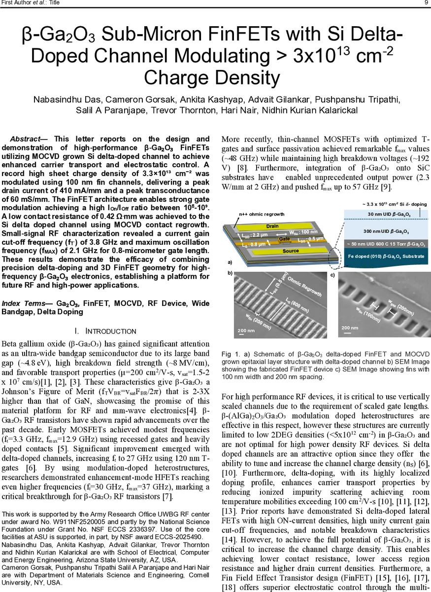
The device fabrication involved defining sub-micron fin structures with a width of 100 nm and a spacing of 200 nm using electron-beam lithography and inductively coupled plasma reactive ion etching. A 7 nm Al2O3 layer deposited by atomic layer deposition served as the gate dielectric, and a 100 nm Ni layer formed the Schottky gate electrode.
Electrical characterization demonstrated outstanding device performance. The FinFET with a 0.8 μm gate length delivered a peak drain current density of 410 mA/mm and a peak transconductance of 60 mS/mm. A key achievement is the exceptionally high on/off current ratio between 10^8 and 10^9, which is maintained despite the very high channel charge density. This is a direct consequence of the FinFET’s wrap-around gate geometry, which provides superior electrostatic control over the channel, effectively suppressing short-channel effects. The pinch-off voltage was measured at -8.3 V, significantly lower than in comparable planar structures, further highlighting the enhanced gate control.
Radio-frequency performance was evaluated through small-signal measurements. The device exhibited a current-gain cutoff frequency (fT) of 3.8 GHz and a maximum oscillation frequency (fMAX) of 2.1 GHz. The authors note that the fMAX is limited by the high resistance of the thin Ni gate, indicating a clear path for improvement through gate metal optimization. Furthermore, the three-terminal off-state breakdown voltage exceeded 200 V, showcasing the device’s potential for high-voltage operation.
In summary, this work successfully demonstrates that integrating MOCVD-grown Si delta-doping with a FinFET architecture effectively addresses critical challenges in beta-Ga2O3 electronics: achieving high charge density, maintaining good carrier transport, ensuring excellent gate control for switching, and enabling promising RF and high-voltage performance. It establishes a robust platform for developing next-generation Ga2O3-based transistors for high-power and high-frequency applications, leveraging the material’s superior theoretical Johnson’s Figure of Merit compared to GaN.
Comments & Academic Discussion
Loading comments...
Leave a Comment