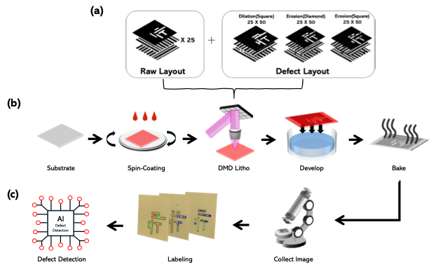
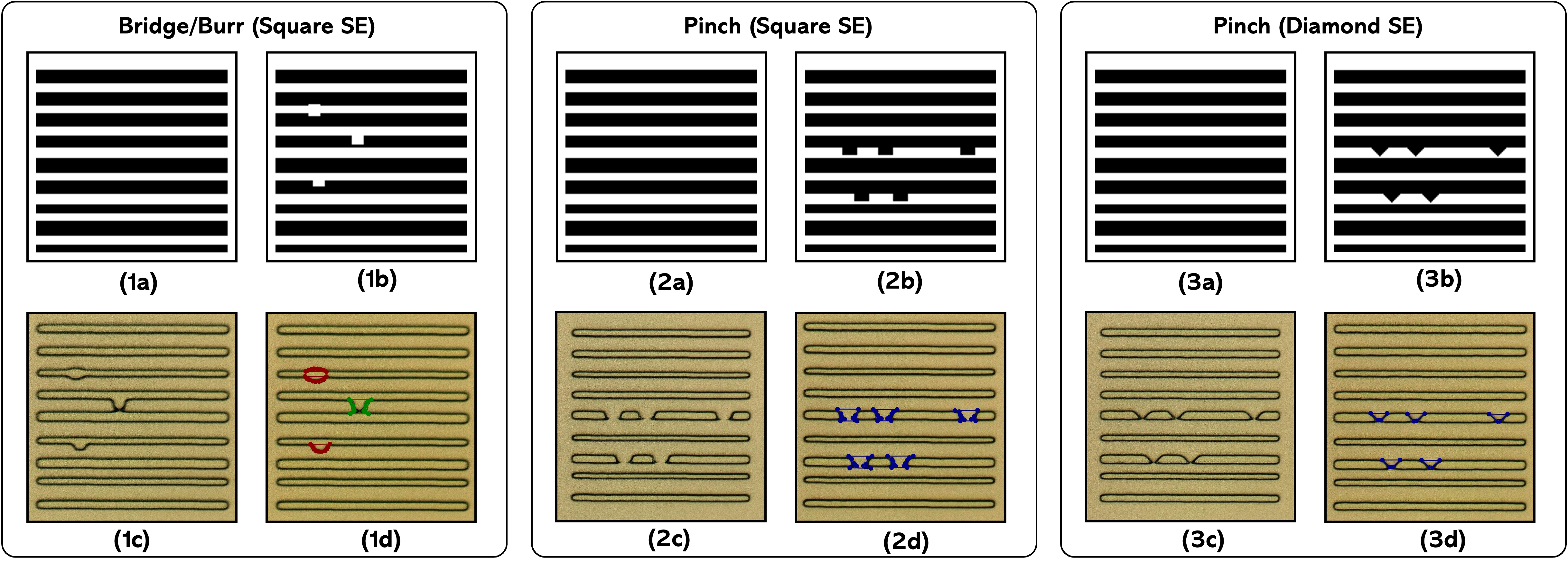
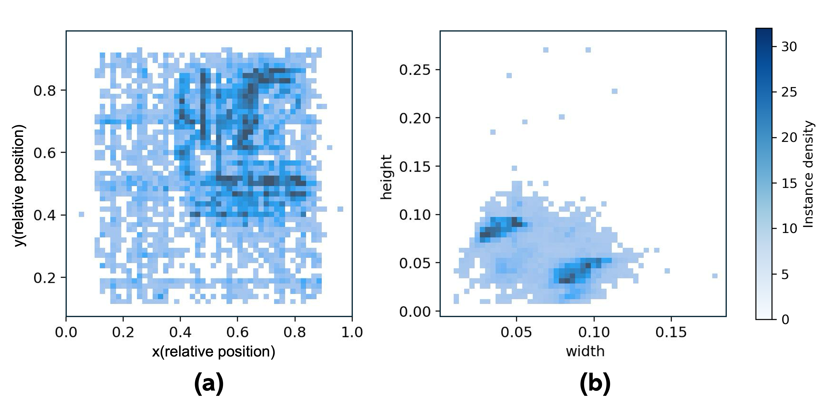
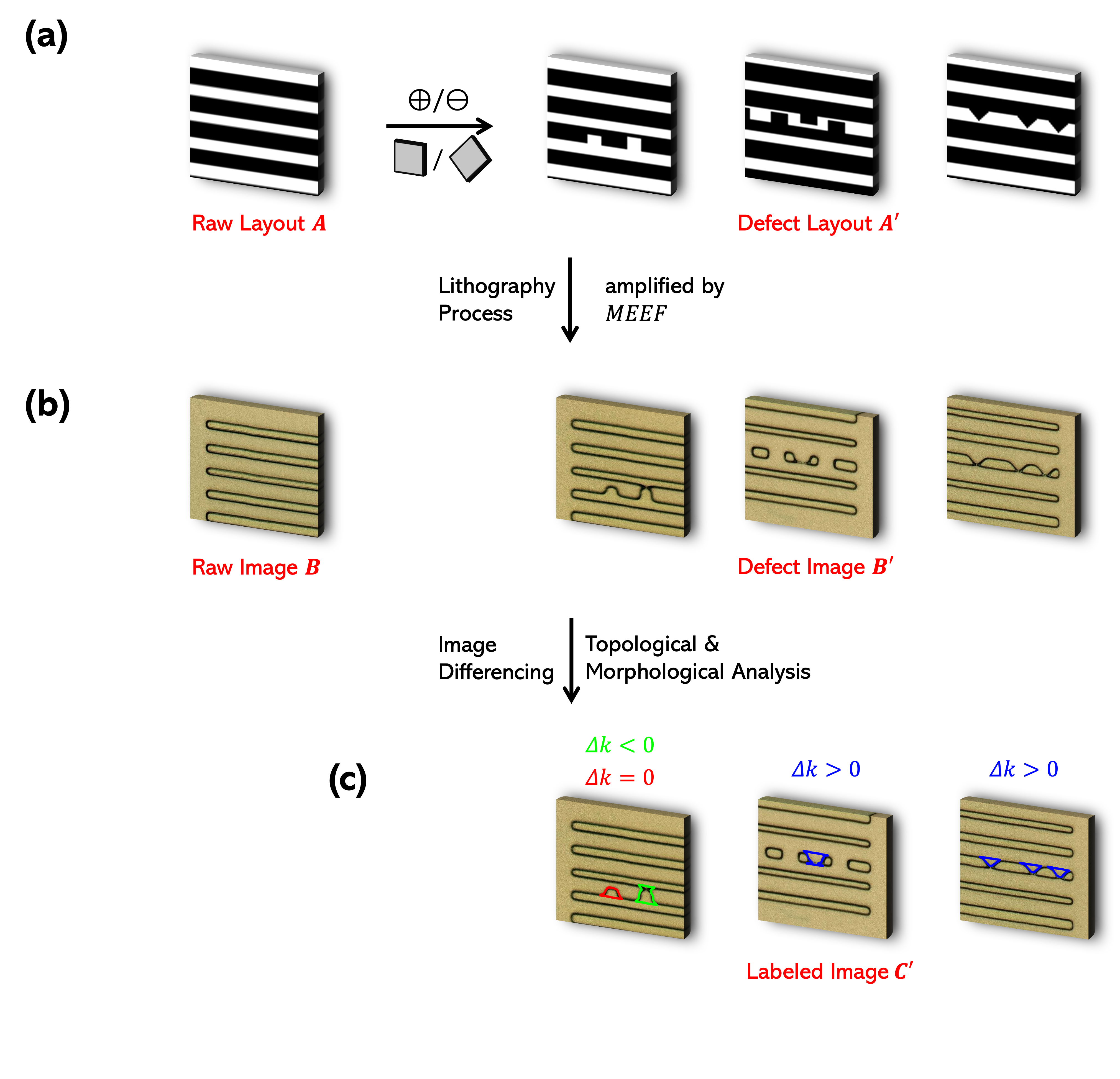
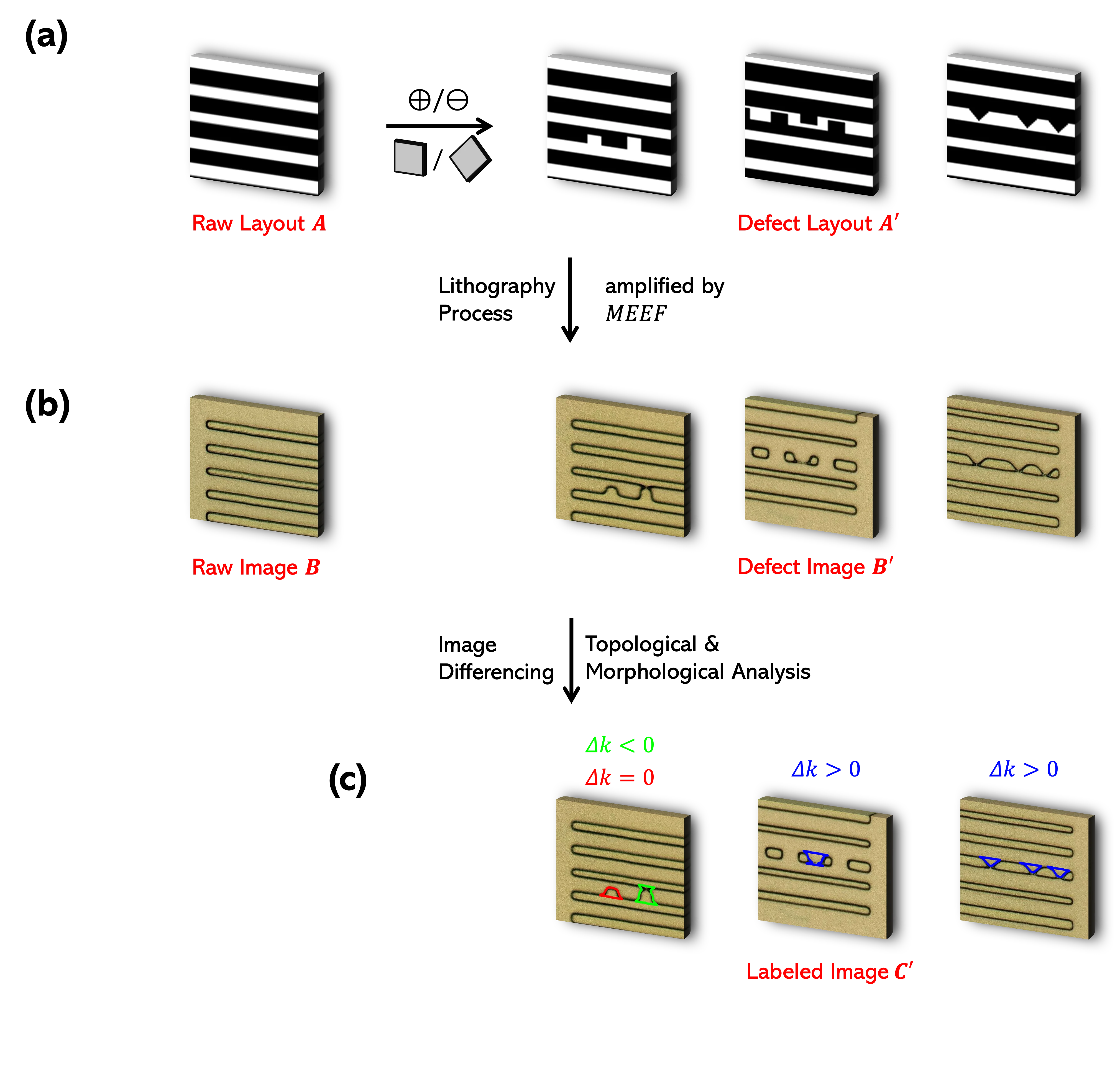
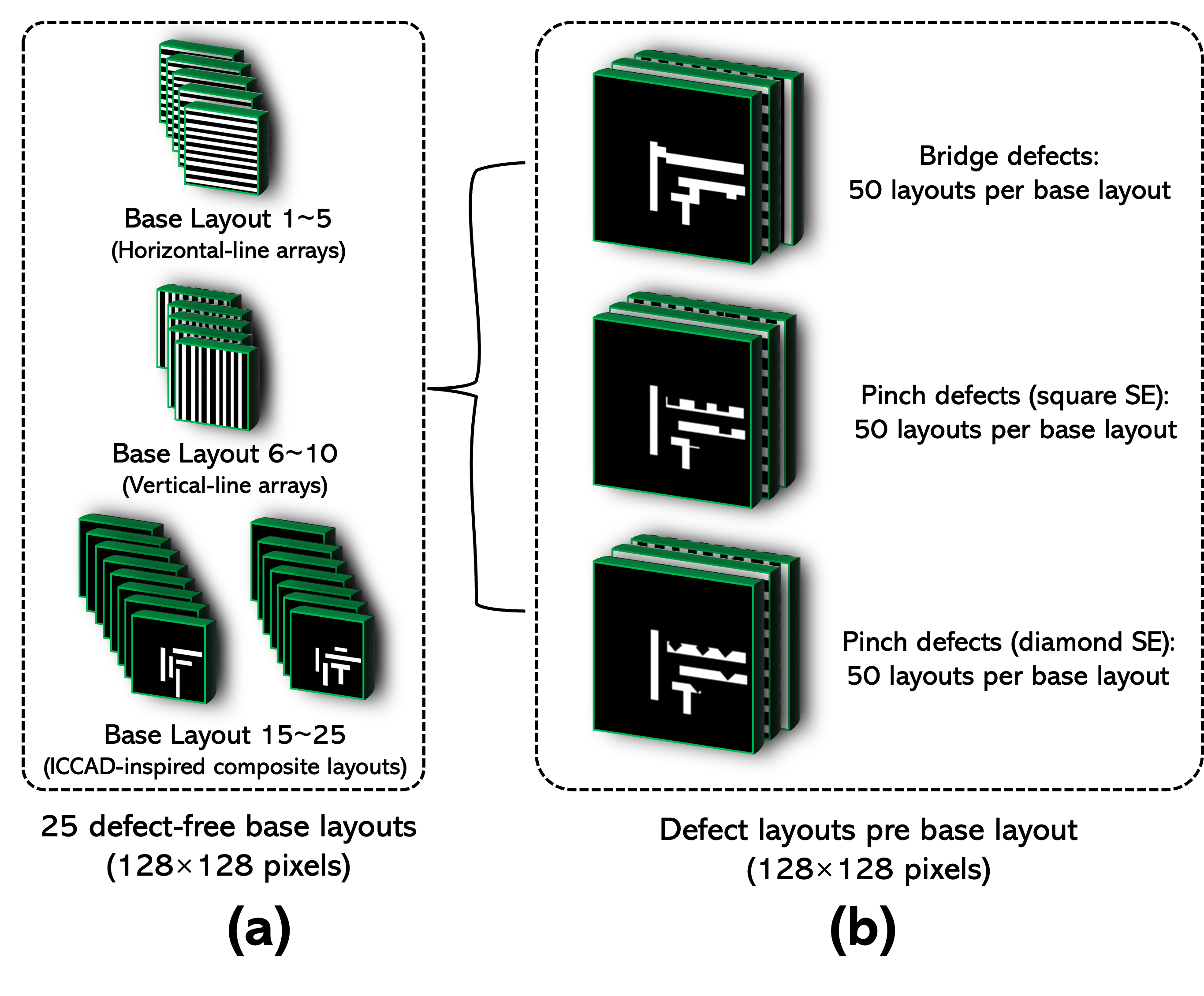
The efficacy of Artificial Intelligence (AI) in micro/nano manufacturing is fundamentally constrained by the scarcity of high-quality and physically grounded training data for defect inspection. Lithography defect data from semiconductor industry are rarely accessible for research use, resulting in a severe shortage of publicly available datasets. To address this bottleneck in lithography, this study proposes a novel methodology for generating large-scale, physically valid defect datasets with pixel-level annotations. The framework begins with the ab initio synthesis of defect layouts using controllable, physics-constrained mathematical morphology operations (erosion and dilation) applied to the original design-level layout. These synthesized layouts, together with their defect-free counterparts, are fabricated into physical samples via high-fidelity digital micromirror device (DMD)-based maskless lithography. Optical microscope images of the synthesized defect samples and their defect-free references are then compared to create consistent defect delineation annotations. Using this methodology, we constructed a comprehensive dataset of 3,530 Optical microscope images containing 13,365 annotated defect instances including four classes: bridge, burr, pinch, and contamination. Each defect instance is annotated with a pixel-accurate segmentation mask, preserving full contour and geometry. The segmentation-based Mask R-
Deep Dive into A Physics-Constrained, Design-Driven Methodology for Defect Dataset Generation in Optical Lithography.
The efficacy of Artificial Intelligence (AI) in micro/nano manufacturing is fundamentally constrained by the scarcity of high-quality and physically grounded training data for defect inspection. Lithography defect data from semiconductor industry are rarely accessible for research use, resulting in a severe shortage of publicly available datasets. To address this bottleneck in lithography, this study proposes a novel methodology for generating large-scale, physically valid defect datasets with pixel-level annotations. The framework begins with the ab initio synthesis of defect layouts using controllable, physics-constrained mathematical morphology operations (erosion and dilation) applied to the original design-level layout. These synthesized layouts, together with their defect-free counterparts, are fabricated into physical samples via high-fidelity digital micromirror device (DMD)-based maskless lithography. Optical microscope images of the synthesized defect samples and their defect
A Physics-Constrained, Design-Driven Methodology for Defect
Dataset Generation in Optical Lithography
Yuehua Hu1,2,†, Jiyeong Kong1,3,†, Dong-yeol Shin1, Jaekyun Kim2,∗, Kyung-Tae
Kang1,∗
1Autonomous Manufacturing & Process R&D Department, Korea Institute of Industrial Technology
(KITECH),
Sangnok-gu, Ansan-si, Gyeonggi-do 15588, Korea
2Department of Photonics and Nanoelectronics, Hanyang University, Ansan-si, Gyeonggi-do 15588, Korea
3Micro/Nano System Department, Korea University, 145 Anam-ro, Seongbuk-gu, Seoul 02841, Korea
†These authors contributed equally to this work.
∗Co-corresponding authors: jeakyunkim@hanyang.ac.kr, ktkang@kitech.re.kr
December 2025
Abstract
The efficacy of Artificial Intelligence (AI) in micro/nano manufacturing is fundamentally constrained
by the scarcity of high-quality and physically grounded training data for defect inspection. Lithography
defect data from semiconductor industry are rarely accessible for research use, resulting in a severe short-
age of publicly available datasets. To address this bottleneck in lithography, this study proposes a novel
methodology for generating large-scale, physically valid defect datasets with pixel-level annotations. The
framework begins with the ab initio synthesis of defect layouts using controllable, physics-constrained math-
ematical morphology operations (erosion and dilation) applied to the original design-level layout. These
synthesized layouts, together with their defect-free counterparts, are fabricated into physical samples via
high-fidelity digital micromirror device (DMD)-based maskless lithography. Optical microscope images of
the synthesized defect samples and their defect-free references are then compared to create consistent defect
delineation annotations. Using this methodology, we constructed a comprehensive dataset of 3,530 Optical
microscope images containing 13,365 annotated defect instances including four classes: bridge, burr, pinch,
and contamination. Each defect instance is annotated with a pixel-accurate segmentation mask, preserving
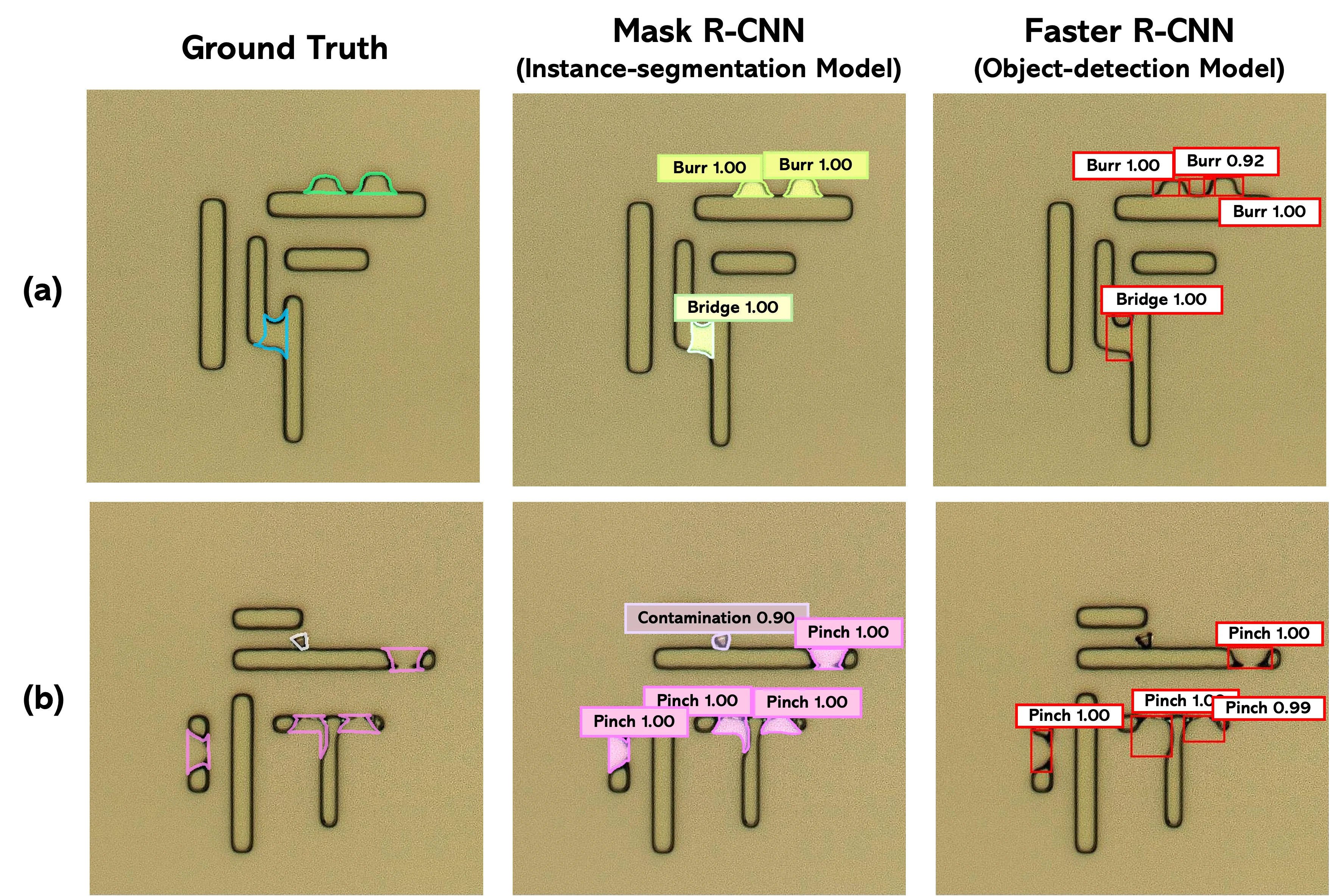
full contour and geometry. The segmentation-based Mask R-CNN achieves AP@0.5 of 0.980, 0.965, and
0.971, compared with 0.740, 0.719, and 0.717 for Faster R-CNN on bridge, burr, and pinch classes, repre-
senting a mean AP@0.5 improvement of approximately 34%. For the contamination class, Mask R-CNN
achieves an AP@0.5 roughly 42% higher than Faster R-CNN. These consistent gains demonstrate that our
proposed methodology to generate defect datasets with pixel-level annotations is feasible for robust AI-based
Measurement/Inspection (MI) in semiconductor fabrication.
1
Introduction
The relentless scaling of Complementary Metal-Oxide-Semiconductor (CMOS) technology has continued
to reduce critical dimensions (CDs) and increase the complexity of the layout [1, 2]. As CDs approach the
nanometer regime, optical lithography, the foundational technique for pattern transfer, encounters fundamental
physical constraints governed by the Rayleigh criterion CD = k1λ/NA [3].
The discrepancy between the
illumination wavelength λ and the target feature size exacerbates Optical Proximity Effects (OPE), leading to
pronounced pattern distortions and substantial degradation in pattern fidelity [4, 5]. These distortions often
manifest as manufacturing defects, including shorts and opens, in layout regions known as lithographic defects
[6, 7, 8].
Lithographic defects refer to localized regions where the printed patterns deviate from the intended design
beyond acceptable process tolerances, which may vary from several nanometers to tens of nanometers depending
on the technology node and specific layer [9, 10]. Although not all defects immediately result in device failure,
they represent critical yield detractors. Unmitigated defects can propagate through downstream steps such as
etching and deposition, eventually causing severe defects that significantly reduce manufacturing yield [11, 12].
Consequently, fast and accurate defect prediction and detection have become essential components of modern
process control and yield management [13].
Artificial Intelligence (AI), particularly Deep Learning (DL), has recently emerged as a powerful tool across
the broad electronics manufacturing landscape, ranging from defect analysis in manufacturing process to perfor-
mance prediction due to its capacity to learn complex spatial patterns and extract subtle features from layout
1
arXiv:2512.09001v1 [cs.CV] 9 Dec 2025
or glass image data [14, 15, 16, 17]. However, the performance of these data-driven approaches is fundamentally
limited by the scarcity of high-quality, accurately annotated training data [10, 14, 18, 19]. Real-world defect
instances are rare, diverse, and difficult to capture at scale, making reliable annotations both labor-intensive
and highly dependent on expert judgment [20, 21].
Furthermore, access to industrial lithography inspection data is strictly limited, and virtually no public
datasets exist for res
…(Full text truncated)…
This content is AI-processed based on ArXiv data.