Advancing Routing-Awareness in Analog ICs Floorplanning
💡 Research Summary
**
The paper tackles the long‑standing challenge of integrating routing awareness into the floorplanning stage of analog integrated circuit (IC) design. Unlike digital layout, analog design imposes strict electrical, topological, and noise constraints, making the placement‑routing interaction highly coupled: a compact floorplan that is difficult to route defeats the purpose of automation. Existing analog layout tools such as MAGICAL and ALIGN rely on analytical or meta‑heuristic floorplanners followed by A* routing, and recent attempts to inject machine‑learning components have struggled to meet industrial standards.
To address this, the authors extend their prior work that combined relational graph convolutional networks (R‑GCN) with reinforcement learning (RL) for analog floorplanning. The new system introduces four major enhancements:
-
Higher‑resolution placement grid – The grid is expanded from 32 × 32 to 256 × 256 cells, providing finer granularity for analog‑specific alignment and symmetry constraints. This increase in state‑action space necessitates a more powerful policy network.
-
U‑Net‑based policy architecture – Replacing the simple CNN used previously, a U‑Net processes the high‑resolution mask images (dead‑space, pin locations, current occupancy) and merges the visual features with the R‑GCN embeddings of the circuit graph. Skip connections and bilinear up‑sampling allow the network to retain both global context and local detail while remaining scalable.
-
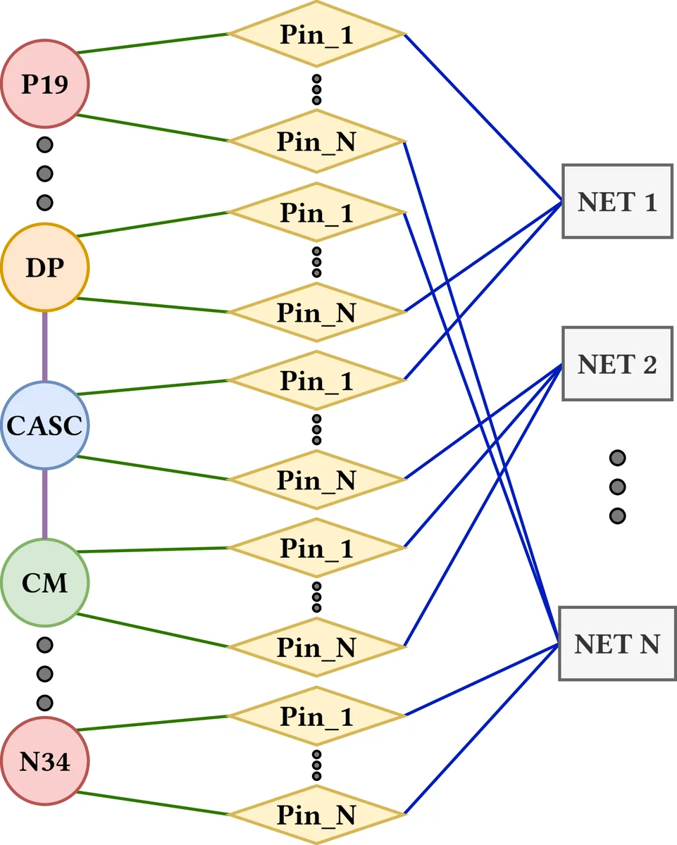
Pin‑enhanced circuit graph – The netlist is represented as a heterogeneous graph where nodes encode devices, sub‑blocks, pins, and nets, and edges capture electrical connections and topological constraints. Pin information is explicitly fed to the R‑GCN, enabling more accurate half‑perimeter wire‑length (HPWL) estimation and giving the RL agent a richer understanding of routing demands.
-
Dynamic Routing Resource (DRR) allocation – Inspired by prior work, the method pads each placed block with a rectangular buffer whose size depends on the number, direction, and distribution of its pins. This buffer reserves routing space proactively, reducing congestion and DRC violations without hard‑coding a fixed clearance.
The reward function is redesigned to prioritize routing‑friendly floorplans. The terminal reward combines three weighted terms: final floorplan area, HPWL (relative to a meta‑heuristic baseline), and deviation from a target aspect ratio. A lexicographic weighting (α ≫ β ≫ γ) forces the agent to first minimize HPWL, then area, then aspect‑ratio error. A large negative penalty (‑1000) is applied for any constraint violation, ensuring strict adherence to design rules.
Training employs Proximal Policy Optimization (PPO) together with a curriculum that starts from small circuits and gradually introduces larger, more diverse designs. The dataset consists of ten analog circuits fabricated in Infineon’s 130 nm commercial node, covering operational transconductance amplifiers, bias circuits, clock resynchronizers, sense amplifiers, delay elements, band‑gap references, and level shifters. Each circuit contains 3–10 functional sub‑blocks and 9–26 individual devices.
To evaluate routing awareness, the authors built a prototype A*‑based detailed router, borrowing concepts from MAGICAL and SA‑GERoute. The router performs rip‑up and reroute up to 35 iterations, supports multiple metal layers, and guarantees DRC‑compliant paths by construction. The router is applied to floorplans generated by the new routing‑aware RL agent and by the baseline R‑GCN RL approaches (both zero‑shot and 1000‑shot fine‑tuned).
Key experimental findings (inter‑quartile mean ± range) on all circuits:
- Failure rate – 9.56 % for the routing‑aware RL, versus 79 % (0‑shot) and 83 % (1000‑shot).
- Total wirelength – 5 497 µm (common subset) compared with 7 108 µm and 6 264 µm for the baselines.
- Via count – 113 (common) versus 118 and 114, indicating more efficient vertical interconnect usage.
- Routing iterations – 3.15 on average (common) versus 10.26 for the 0‑shot baseline, showing faster convergence.
On the most complex 24‑block delay‑line circuit, the routing‑aware method succeeded in 76 % of runs, achieving a mean routing time of 48.7 s, while the prior methods failed to produce any fully routable layout. The dynamic DRR padding and HPWL‑driven placement were identified as the primary contributors to this success.
In conclusion, by integrating fine‑grained placement, pin‑aware graph embeddings, dynamic routing resource estimation, and a routing‑centric reward, the authors demonstrate a substantial leap in analog floorplanning quality. The approach yields markedly lower dead‑space (13.8 % reduction), shorter wirelength (40.6 % reduction), and dramatically higher routing success (up to 73 % improvement) compared with state‑of‑the‑art learning‑based methods. The paper suggests future work on closing the loop between the router and the RL agent, enabling true joint optimization of placement and routing for analog ICs.
Comments & Academic Discussion
Loading comments...
Leave a Comment