Accelerating PageRank Algorithmic Tasks with a new Programmable Hardware Architecture
Addressing the growing demands of artificial intelligence (AI) and data analytics requires new computing approaches. In this paper, we propose a reconfigurable hardware accelerator designed specifically for AI and data-intensive applications. Our architecture features a messaging-based intelligent computing scheme that allows for dynamic programming at runtime using a minimal instruction set. To assess our hardware’s effectiveness, we conducted a case study in TSMC 28nm technology node. The simulation-based study involved analyzing a protein network using the computationally demanding PageRank algorithm. The results demonstrate that our hardware can analyze a 5,000-node protein network in just 213.6 milliseconds over 100 iterations. These outcomes signify the potential of our design to achieve cutting-edge performance in next-generation AI applications.
💡 Research Summary
The paper presents a novel reconfigurable hardware accelerator specifically tailored for artificial‑intelligence (AI) and data‑intensive workloads. Recognizing the limitations of existing FPGA‑based and coarse‑grained reconfigurable array (CGRA) solutions—namely high interconnect overhead, limited runtime reconfigurability, and separate instruction and data memories—the authors introduce a “messaging‑based programmable hardware” architecture that fuses data and control into a single compact message.
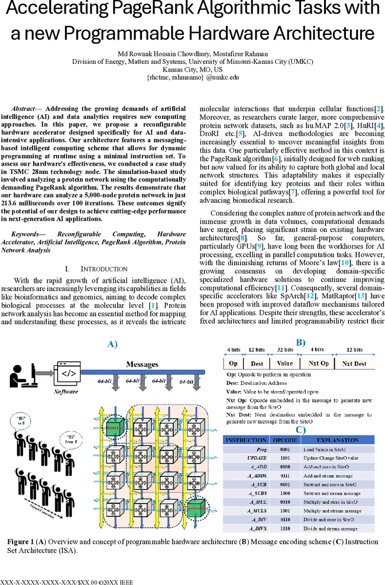
The core of the design is a minimal 10‑instruction set architecture (ISA). One instruction, “Prog,” loads floating‑point operands into a processing element (PE), while the remaining nine instructions (UPDATE, A_ADD, A_SUB, A_MUL, A_DIV, A_ADDS, A_SUBS, A_MULS, A_DIVS) perform various arithmetic operations and updates. Each 64‑bit message encodes an opcode (bits 0‑3), a destination address (bits 4‑15), and operand payloads. PEs are organized in a 2‑D grid (illustrated as a 4 × 4 array) and are capable of routing messages either rightward or downward based on the destination field, effectively creating virtual links between any two units without explicit compile‑time routing tables. This approach eliminates the need for distinct instruction and data memories, dramatically reducing network‑on‑chip (NoC) complexity and power consumption.
A key contribution is the hardware‑level matrix‑vector multiplication (MVM) pipeline. The matrix A (size N × M) is “hopped” row‑by‑row across the grid; each row of PEs stores one matrix row. The vector B (size M × 1) is broadcast via a vertical bus, and each PE multiplies its stored matrix elements with the corresponding vector component in a single clock cycle. The partial products are then summed across the row using a horizontal bus, and the final result is off‑loaded after an additional cycle. The total number of time steps for an MVM operation is N + 3, essentially linear in the number of rows and independent of column count or vector length.
To demonstrate practical impact, the authors implement the PageRank algorithm—a computation‑heavy iterative method widely used for ranking nodes in graphs—on a protein‑interaction network. Each iteration consists of (i) an MVM (N + 3 steps), (ii) a scalar multiplication with the damping factor (1 step), and (iii) addition and off‑load (2 steps). For n iterations the total steps become n × (N + 6). Using a 200 MHz clock, a 28 nm TSMC HPC+ process, and 4,096 PEs, the accelerator processes a 5,000‑node protein network for 100 PageRank iterations in 213.6 ms. Power per PE is measured at 4.1 mW, and the entire design occupies roughly 98 k gates.
The paper’s contributions can be summarized as follows:
- Programmable Messaging Paradigm – By embedding both control and data in a single message, the architecture achieves runtime reconfigurability without a separate compiler‑generated routing schedule.
- Compact ISA – A ten‑instruction set suffices for a wide range of arithmetic kernels, simplifying hardware control logic while retaining flexibility.
- Efficient MVM Engine – The N + 3 step pipeline provides near‑optimal latency for dense linear algebra, a critical bottleneck in many AI algorithms.
- Empirical Validation – Silicon‑level simulations in a 28 nm node confirm low latency, modest power, and high throughput on a real‑world PageRank workload.
Nevertheless, the study has limitations. The experimental platform is confined to a 16‑PE (4 × 4) prototype; scaling to larger arrays may expose routing contention, bus saturation, or timing closure challenges not captured in the current simulations. Moreover, the ISA focuses on floating‑point arithmetic; extending support to integer‑based kernels, non‑linear functions (e.g., activation functions), or mixed‑precision operations would be necessary for broader AI applicability.
In conclusion, the messaging‑based programmable hardware architecture offers a compelling middle ground between fully custom ASICs and flexible but inefficient CGRAs/FPGAs. Its ability to reprogram at runtime through lightweight messages, combined with a linear‑time matrix‑vector engine, promises significant performance and energy benefits for AI and data‑intensive tasks, positioning it as a promising direction for next‑generation accelerator design.
Comments & Academic Discussion
Loading comments...
Leave a Comment