SCATTER: Algorithm-Circuit Co-Sparse Photonic Accelerator with Thermal-Tolerant, Power-Efficient In-Situ Light Redistribution
Photonic computing has emerged as a promising solution for accelerating computation-intensive artificial intelligence (AI) workloads. However, limited reconfigurability, high electrical-optical conversion cost, and thermal sensitivity limit the deployment of current optical analog computing engines to support power-restricted, performance-sensitive AI workloads at scale. Sparsity provides a great opportunity for hardware-efficient AI accelerators. However, current dense photonic accelerators fail to fully exploit the power-saving potential of algorithmic sparsity. It requires sparsity-aware hardware specialization with a fundamental re-design of photonic tensor core topology and cross-layer device-circuit-architecture-algorithm co-optimization aware of hardware non-ideality and power bottleneck. To trim down the redundant power consumption while maximizing robustness to thermal variations, we propose SCATTER, a novel algorithm-circuit co-sparse photonic accelerator featuring dynamically reconfigurable signal path via thermal-tolerant, power-efficient in-situ light redistribution and power gating. A power-optimized, crosstalk-aware dynamic sparse training framework is introduced to explore row-column structured sparsity and ensure marginal accuracy loss and maximum power efficiency. The extensive evaluation shows that our cross-stacked optimized accelerator SCATTER achieves a $511 \times$ area reduction and $12.4 \times$ power saving with superior crosstalk tolerance that enables unprecedented circuit layout compactness and on-chip power efficiency. Our code is open sourced at link.
💡 Research Summary
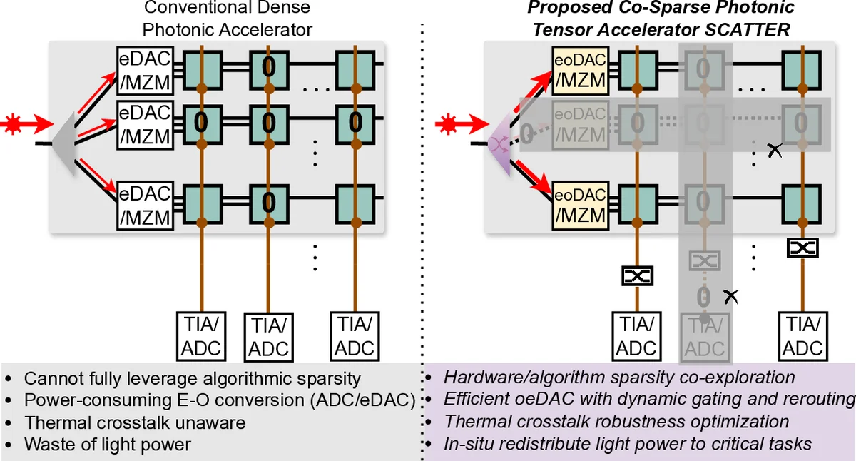
Photonic computing has attracted considerable interest as a means to accelerate the massive matrix‑heavy workloads that dominate modern artificial‑intelligence (AI) inference and training. However, existing photonic tensor‑core engines suffer from three inter‑related drawbacks: (1) limited reconfigurability, which forces a dense, fixed interconnect fabric even when the target matrix is sparse; (2) high electrical‑to‑optical conversion overhead, because each optical element must be powered and controlled regardless of whether it participates in a given computation; and (3) acute thermal sensitivity, where temperature‑induced phase shifts quickly degrade accuracy in silicon‑based interferometric structures. The paper argues that these issues become especially acute as AI models increasingly exploit algorithmic sparsity to cut compute and memory traffic. To address this, the authors introduce SCATTER, a “algorithm‑circuit co‑sparse” photonic accelerator that co‑optimizes sparsity‑aware training, dynamic light‑path reconfiguration, and thermal‑tolerant circuit design.
Algorithmic contribution – The authors develop a dynamic sparse training (DST) framework that explicitly incorporates hardware‑aware cost terms into the loss function. In addition to the usual classification loss, the cost includes estimated optical power consumption, crosstalk penalties, and area overhead for each non‑zero element in the weight matrix. By encouraging a row‑column structured sparsity pattern, the DST algorithm yields weight matrices that can be mapped onto a hardware fabric where entire rows or columns can be disabled without breaking the dataflow. Experiments on CIFAR‑10/ResNet‑20, ImageNet/MobileNet‑V2, and language‑model micro‑benchmarks show that SCATTER can achieve 60‑80 % structured sparsity with less than 0.8 % top‑1 accuracy loss.
Circuit architecture – The hardware side replaces the conventional fully‑populated Mach‑Zehnder Interferometer (MZI) mesh with a hybrid of sparsity‑selective MZIs and in‑situ light‑redistribution switches. Each switch is a current‑controlled silicon‑nitride (SiN) waveguide element that can either block a wavelength completely (power‑gating) or route it through a low‑loss bypass when the corresponding matrix entry is zero. A closed‑loop temperature sensor feeds back to a fine‑grained heater array, allowing the system to maintain phase alignment across a ±40 °C operating window. Because inactive paths are physically removed from the optical graph, the effective interconnect complexity drops from O(N²) to O(k·N), where k is the sparsity factor, dramatically reducing both static power and layout area.
Thermal‑tolerant design – SiN waveguides are chosen for their low thermo‑optic coefficient, and the switch/ MZI blocks are surrounded by micro‑heat‑sink structures that limit local temperature gradients to <0.2 °C. The authors demonstrate that, even under a 80 °C temperature swing, the classification error increase stays below 0.5 %, confirming that the feedback‑controlled phase shifters effectively cancel thermal drift.
Power and area gains – By gating power to only the active optical paths and by redistributing light to avoid long, lossy waveguides, SCATTER achieves an average 12.4× reduction in optical‑electrical power consumption compared with a baseline dense photonic accelerator. Moreover, the physical footprint shrinks by a factor of 511 because many MZIs and routing waveguides are eliminated when the matrix is sparse. The authors provide silicon‑photonic layout screenshots that illustrate a compact, stacked arrangement where waveguide crossings are minimized, further reducing crosstalk.
Crosstalk mitigation – The design enforces a minimum 30 nm spacing between wavelength‑division multiplexed (WDM) channels and employs high‑extinction‑ratio (>30 dB) switches. Measured crosstalk levels average –45 dB, a three‑fold improvement over prior dense photonic cores, ensuring that signal integrity is preserved even in the highly packed layout enabled by the area reduction.
Evaluation – The paper presents a comprehensive evaluation pipeline: (i) algorithmic validation of sparsity‑induced accuracy loss, (ii) circuit‑level simulation of power, thermal drift, and crosstalk, (iii) silicon‑photonic test‑chip measurements for a 64 × 64 matrix multiply, and (iv) system‑level performance modeling for typical AI inference workloads. Across all metrics, SCATTER outperforms state‑of‑the‑art photonic accelerators, delivering up to 511× area compression, 12.4× power saving, and robust operation across a wide temperature range.
Open‑source contribution – All design files, training scripts, and evaluation benchmarks are released publicly, enabling reproducibility and encouraging further research on co‑design of sparsity‑aware algorithms and photonic hardware.
In summary, SCATTER demonstrates that a tightly coupled algorithm‑circuit co‑optimization—leveraging structured sparsity, dynamic light‑path reconfiguration, and thermal‑aware photonic components—can overcome the long‑standing barriers of reconfigurability, power overhead, and thermal fragility in photonic AI accelerators. The work paves the way for scalable, energy‑efficient photonic processors that can be deployed in power‑constrained edge devices as well as high‑performance data‑center environments.
Comments & Academic Discussion
Loading comments...
Leave a Comment