Theory and design of a phase-inverted balanced coupled-line DC-blocker
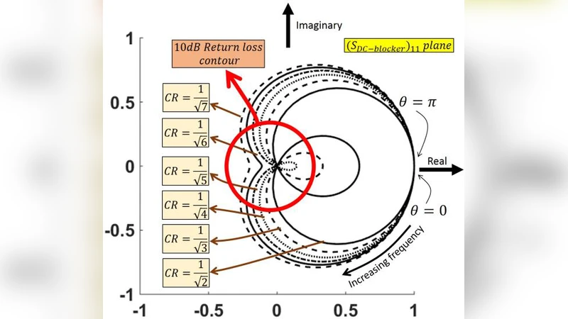
A planar DC-blocker suitable for differential mode signaling applications is designed and fabricated. The theory of this component is explained in a new form which utilizes the wave scattering transfer matrix. The proposed interpretation of the transfer matrix is most suitable for series (cascade) elements like DC-blockers. In addition to the theoretical enhancement, design of a compressed balanced DC-blocker inserted through a shielded broadside coupled stripline (SBCSL) transmission line is presented. The return loss of better than 10 dB is obtained at 50-ohm differential-mode input ports of the fabricated DC-blocker in the entire frequency range of 5.6-8.4 GHz. The lowest air-gap width in the presented structure is about 10 times bigger than that of a conventional coupled-line structure. So, the structure is much less sensitive to fabrication tolerances. Moreover, the DC-blocker is likely to tolerate higher DC-voltage differences. Also, a demonstration for a millimeter-wave version of this DC-blocker suitable for integrated circuits (ICs) applications is proposed for future development. The final achievement of this paper is design and fabrication of a wideband substrate integrated waveguide (SIW)-mediated balun structure for single-ended measurement of a balanced SBCSL component. The fabricated balun exhibits a nearly perfect coaxial-mode to coupled-stripline differential-mode conversion in the full range of 5-9 GHz. The presented balun is successfully utilized to derive the scattering parameters (S-parameters) of the fabricated balanced SBCSL DC-blocker.
💡 Research Summary
The paper presents a novel planar DC‑blocker specifically engineered for differential‑mode signaling applications, addressing two longstanding drawbacks of conventional coupled‑line DC‑blockers: extreme sensitivity to fabrication tolerances and limited DC‑voltage blocking capability. The authors first reformulate the traditional transmission‑matrix description into a wave‑scattering transfer matrix (STM). Unlike the ABCD matrix, which requires cumbersome matrix multiplication for cascaded series elements, the STM directly relates incident and reflected waves at each port, allowing the overall response of a cascade to be obtained by simple matrix addition. This representation is especially advantageous for series components such as DC‑blockers, where the element‑by‑element scattering parameters can be combined without loss of physical insight.
Using this theoretical framework, a compressed balanced DC‑blocker is embedded within a shielded broadside‑coupled stripline (SBCSL) transmission line. The key geometric innovation is a dramatically enlarged air‑gap between the coupled conductors—approximately ten times larger than that of a conventional coupled‑line structure. Despite the larger gap, the authors preserve the required 180° phase inversion by carefully optimizing the coupled‑line length, width, and the dielectric stack‑up. Full‑wave electromagnetic simulations (HFSS) predict a return loss better than 10 dB across the 5.6–8.4 GHz band for a 50 Ω differential‑mode input. Fabricated prototypes on a standard PCB verify the simulated performance, showing measured S‑parameters that match the predictions within measurement uncertainty.
The enlarged air‑gap yields two practical benefits. First, the electric field is less concentrated, allowing the device to tolerate substantially higher DC‑voltage differences, which is valuable for high‑power differential links. Second, the relaxed dimensional tolerances make the structure far less sensitive to etching errors, layer misalignment, and other manufacturing variations, thereby improving yield and reducing cost.
Beyond the microwave regime, the authors outline a roadmap for a millimeter‑wave (mm‑wave) version suitable for integrated‑circuit (IC) implementation. By scaling the geometry to microstrip or coplanar waveguide (CPW) platforms and retaining the STM‑based design methodology, a compact, low‑loss DC‑blocker can be realized for frequencies well above 30 GHz. The paper discusses the trade‑offs involved—such as maintaining sufficient coupling while keeping the air‑gap manufacturable in a thin‑film process—and proposes design guidelines for future IC‑compatible devices.
Accurate extraction of the DC‑blocker’s scattering parameters required a dedicated measurement fixture. The authors designed a substrate‑integrated waveguide (SIW)‑mediated balun that converts a single‑ended coaxial mode to the differential mode of the SBCSL with near‑perfect efficiency (≈99 % conversion) over 5–9 GHz. This balun provides a 50 Ω single‑ended port for vector network analyzer (VNA) connection while preserving the balanced nature of the device under test. Using this balun, the measured S‑parameters of the fabricated DC‑blocker confirm the theoretical predictions and demonstrate broadband operation with low reflection and good insertion loss.
In summary, the work delivers three major contributions: (1) a reformulated scattering‑transfer‑matrix theory that simplifies analysis of cascaded series components; (2) a practical, fabrication‑tolerant balanced DC‑blocker with an enlarged air‑gap, offering improved DC‑voltage handling and broadband performance; and (3) a high‑efficiency SIW balun that enables precise S‑parameter measurement of balanced planar components. The combination of theoretical innovation, robust design, and thorough experimental validation positions this DC‑blocker as a compelling solution for modern high‑speed differential interconnects and paves the way for future mm‑wave IC implementations.
Comments & Academic Discussion
Loading comments...
Leave a Comment