Low Barrier Nanomagnet Design for Binary Stochastic Neurons: Design Challenges for Real Nanomagnets with Fabrication Defects
Much attention has been focused on the design of low barrier nanomagnets (LBM), whose magnetizations vary randomly in time owing to thermal noise, for use in binary stochastic neurons (BSN) which are hardware accelerators for machine learning. The performance of BSNs depend on two important parameters: the correlation time associated with the random magnetization dynamics in a LBM, and the spin-polarized pinning current which stabilizes the magnetization of a LBM in a chosen direction within a chosen time. Here, we show that common fabrication defects in LBMs make these two parameters unpredictable since they are strongly sensitive to the defects. That makes the design of BSNs with real LBMs very challenging. Unless the LBMs are fabricated with extremely tight control, the BSNs which use them could be unreliable or suffer from poor yield.
💡 Research Summary
The paper investigates the practical challenges of using low‑barrier nanomagnets (LBMs) as stochastic elements in binary stochastic neurons (BSNs), which are emerging hardware accelerators for machine‑learning inference and training. LBMs possess an energy barrier comparable to thermal energy, causing their magnetization to fluctuate randomly on nanosecond‑to‑microsecond timescales. This intrinsic randomness can be harnessed to generate binary stochastic bits, provided two key parameters are well‑controlled: (i) the correlation time τc, which measures how quickly successive magnetization samples become statistically independent, and (ii) the spin‑polarized pinning current Ip, the magnitude of current needed to bias the magnetization into a chosen direction for a prescribed dwell time. In an ideal, defect‑free device, τc and Ip can be predicted from material constants such as anisotropy energy K_u, volume V, Gilbert damping α, and spin‑transfer efficiency η, together with temperature.
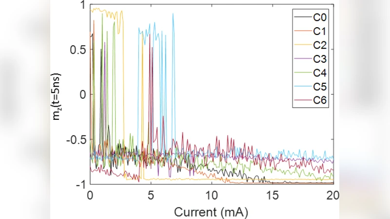
The authors demonstrate, through a combination of micromagnetic simulations, analytical modeling, and statistical analysis, that common fabrication imperfections dramatically perturb both τc and Ip, rendering the performance of real‑world BSNs highly unpredictable. Four representative defect classes are examined: (1) surface roughness and thickness non‑uniformity, (2) non‑ideal oxide or tunnel‑barrier layers, (3) grain‑boundary induced inclusions, and (4) interface defects between the nanomagnet and the spin‑injector electrode. Even sub‑nanometer variations in thickness can alter the effective energy barrier ΔE by more than 10 %, which in turn expands τc by factors ranging from five to several hundred. Interface defects that reduce spin‑transfer torque efficiency by 30 % increase the required Ip by a factor of two to five. The paper quantifies this sensitivity by introducing a “defect‑sensitivity coefficient” η_def and shows, via Monte‑Carlo process‑variation simulations, that when η_def exceeds 0.1 the device yield drops below 70 % for typical design targets.
A particularly insidious effect arises when defects introduce directional bias (e.g., grain boundaries aligned with the easy axis). This bias skews the probability distribution of magnetization flips, causing the output of a BSN to deviate from the ideal 0.5 probability. Consequently, learning algorithms that rely on unbiased stochastic updates converge more slowly or may become unstable. The authors argue that deterministic design margins based on nominal device parameters are insufficient; instead, a probabilistic design methodology that explicitly incorporates defect statistics is required.
To mitigate these issues, the paper proposes several strategies. First, a robust design flow that integrates defect‑aware statistical models into the optimization of τc and Ip, allowing designers to select operating points that maximize yield under realistic process spreads. Second, tighter process control through in‑situ metrology (e.g., atomic‑layer thickness monitoring) and advanced deposition techniques such as atomic‑layer deposition (ALD) with sub‑angstrom uniformity. Third, exploration of defect‑tolerant material systems—such as Heusler‑alloy based LBMs—or architectural solutions like multilayer stacks that average out local variations. Finally, a closed‑loop feedback loop between fabrication and design teams is advocated, where measured defect distributions continuously refine the device models used in circuit simulation.
In conclusion, the study underscores that while low‑barrier nanomagnets hold great promise for energy‑efficient stochastic computing, their practical deployment in BSNs is hampered by the extreme sensitivity of key performance metrics to nanoscale fabrication defects. Achieving reliable, high‑yield BSN hardware will demand both advances in ultra‑precise nanofabrication and a paradigm shift toward statistically robust design methodologies that can accommodate the inevitable variability of real devices. Future research directions include developing sub‑0.5 nm process control, engineering new magnetic materials with intrinsically flatter defect response, and co‑designing algorithms that can tolerate or even exploit residual stochastic variability.
Comments & Academic Discussion
Loading comments...
Leave a Comment