On-Chip Error-triggered Learning of Multi-layer Memristive Spiking Neural Networks
Recent breakthroughs in neuromorphic computing show that local forms of gradient descent learning are compatible with Spiking Neural Networks (SNNs) and synaptic plasticity. Although SNNs can be scalably implemented using neuromorphic VLSI, an architecture that can learn using gradient-descent in situ is still missing. In this paper, we propose a local, gradient-based, error-triggered learning algorithm with online ternary weight updates. The proposed algorithm enables online training of multi-layer SNNs with memristive neuromorphic hardware showing a small loss in the performance compared with the state of the art. We also propose a hardware architecture based on memristive crossbar arrays to perform the required vector-matrix multiplications. The necessary peripheral circuitry including pre-synaptic, post-synaptic and write circuits required for online training, have been designed in the sub-threshold regime for power saving with a standard 180 nm CMOS process.
💡 Research Summary
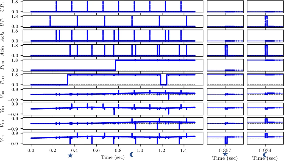
The paper presents a complete solution for on‑chip learning in multi‑layer spiking neural networks (SNNs) built on memristive cross‑bar arrays (RCAs). Recognizing that conventional back‑propagation requires non‑local error signals and incurs prohibitive routing and memory costs in neuromorphic hardware, the authors introduce an “error‑triggered learning” framework that is both spatially and temporally local. Each layer is equipped with a local loss function; the gradient with respect to the weight matrix is factorized into three terms: a local error (δ), a surrogate derivative of the spiking non‑linearity (B), and the pre‑synaptic trace (P). The local error is quantized by a tunable threshold θ into integer events E = sign(δ)·⌊|δ|/θ⌋. An update occurs only when the membrane potential lies within a narrow surrogate window (u⁻ < U < u⁺) and the binarized pre‑synaptic trace ˜P = Θ(P‑p̄) equals one. The weight change therefore becomes ΔW = –η̃·E·B·˜P, which is ternary (–η̃, 0, +η̃). This ternary update maps directly onto memristor devices that can be programmed with positive or negative voltage pulses, eliminating the need for high‑resolution DACs or analog weight storage.
Algorithmically, the method avoids full back‑propagation across layers. For hidden layers, the authors adopt deep local losses (e.g., random‑fixed projections followed by a mean‑squared error) and employ feedback alignment with a random matrix H to approximate the transpose required for error propagation. The error events E can be generated either by an auxiliary spiking network or by a conventional processor; the paper remains agnostic to the exact implementation, requiring only that the events be delivered to the corresponding neuron within one time step.
The hardware architecture consists of four main blocks: (1) a memristive cross‑bar that performs the vector‑matrix multiplication (VMM) in a single analog step; (2) a pre‑synaptic integrator that accumulates incoming spikes into the trace P; (3) a post‑synaptic circuit that adds the weighted current from the cross‑bar to the membrane potential U, applies the surrogate derivative B, and generates output spikes; (4) a write driver that, upon receiving an error event E and a high ˜P, issues a positive or negative programming pulse to the selected memristor cell. All peripheral circuits are designed in the sub‑threshold region of a 180 nm CMOS process to minimize static power. The write driver incorporates pulse‑width modulation to realize the learning rate η̃ and to compensate for device non‑linearity.
Simulation results are presented on MNIST and N‑MNIST benchmarks using two‑ and three‑layer SNNs. The proposed method achieves classification accuracies within 1–2 % of state‑of‑the‑art surrogate‑gradient approaches, while reducing the total number of weight updates by up to 88×. Circuit‑level simulations in Cadence Spectre show an average neuron power consumption of ~0.8 µW and an energy cost of ~45 pJ per ternary weight update. The full core occupies approximately 0.12 mm² in the 180 nm process, demonstrating a compact footprint.
The authors discuss limitations: reliance on local loss functions may hinder performance on tasks requiring deep credit assignment; external computation of error events introduces latency and additional power overhead; and memristor variability and non‑idealities are only partially mitigated by the simple ternary scheme. Future work includes integrating a fully on‑chip error‑computation unit, exploring robustness to device mismatch, and scaling the design to more advanced CMOS nodes (e.g., 28 nm) to further improve energy‑area efficiency.
In summary, the paper bridges the gap between mathematically rigorous gradient‑based learning and practical neuromorphic hardware by introducing a ternary, error‑triggered learning rule that is naturally compatible with memristive cross‑bars and ultra‑low‑power CMOS peripherals, offering a promising path toward scalable, lifelong learning on silicon.
Comments & Academic Discussion
Loading comments...
Leave a Comment