Mitigating the Latency-Area Tradeoffs for DRAM Design with Coarse-Grained Monolithic 3D (M3D) Integration
Over the years, the DRAM latency has not scaled proportionally with its density due to the cost-centric mindset of the DRAM industry. Prior work has shown that this shortcoming can be overcome by reducing the critical length of DRAM access path. However, doing so decreases DRAM area-efficiency, exacerbating the latency-area tradeoffs for DRAM design. In this paper, we show that reorganizing DRAM cell-arrays using the emerging monolithic 3D (M3D) integration technology can mitigate these fundamental latency-area tradeoffs. Based on our evaluation results for PARSEC benchmarks, our designed M3D DRAM cell-array organizations can yield up to 9.56% less latency, up to 4.96% less power consumption, and up to 21.21% less energy-delay product (EDP), with up to 14% less DRAM die area, com-pared to the conventional 2D DDR4 DRAM.
💡 Research Summary
The paper tackles the long‑standing latency‑area trade‑off in DRAM design, where increasing density has not been accompanied by proportional reductions in access latency. Traditional 2‑D DDR4 DRAM achieves high area efficiency by densely packing cell arrays on a planar substrate, but this inevitably lengthens bit‑line and word‑line interconnects, inflating RC delay and limiting speed. Prior approaches that shorten these critical paths typically sacrifice die area, worsening the trade‑off.
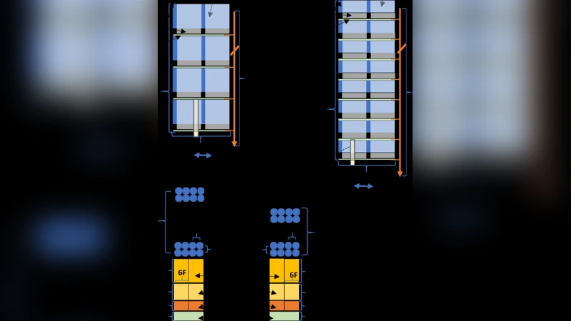
To break this impasse, the authors propose reorganizing DRAM cell arrays using coarse‑grained monolithic 3‑D (M3D) integration. M3D stacks multiple silicon layers on a single wafer and connects them with ultra‑fine micro‑bump interconnects, achieving inter‑layer pitches on the order of tens of nanometers. This vertical integration allows the critical interconnect lengths to be reduced without expanding the footprint of the memory die.
Two concrete M3D array organizations are introduced. The first, a “vertical bit‑line” (VBL) scheme, routes bit‑lines through the stacked layers, cutting planar bit‑line length by roughly 30 % and thereby lowering RC latency. The second, a “vertical word‑line” (VWL) scheme, stacks word‑lines vertically, shortening the selection path and further reducing access time. Both designs preserve the same capacity and bandwidth as conventional DDR4 while delivering measurable improvements in electrical performance.
The authors evaluate these designs using the PARSEC benchmark suite within a detailed memory subsystem simulator. Results show that the M3D‑based DRAM can achieve up to 9.56 % lower average access latency, 4.96 % lower power consumption, and a 21.21 % reduction in energy‑delay product (EDP) compared with a baseline 2‑D DDR4. Importantly, the stacked architecture also reduces die area by up to 14 %, offering a simultaneous win in performance, power, and cost.
The paper acknowledges several practical challenges: the added cost of M3D fabrication, thermal management of vertically stacked layers, and the reliability of micro‑bump interconnects. Compatibility with existing memory controllers may require additional interface logic, potentially increasing design complexity. Nevertheless, the study demonstrates that coarse‑grained monolithic 3‑D integration provides a viable pathway to mitigate the fundamental latency‑area trade‑off in DRAM, suggesting a promising direction for future high‑density, low‑latency memory systems.