A Unified Hardware Architecture for Convolutions and Deconvolutions in CNN
💡 Research Summary
This paper presents a scalable FPGA accelerator architecture that jointly handles convolution and deconvolution operations within a single, shared process‑element (PE) array, targeting semantic‑segmentation networks such as SegNet‑Basic. The authors first motivate the need for efficient deconvolution acceleration, noting that most existing FPGA designs focus on convolution while treating deconvolution as a secondary, often bottleneck‑inducing step.
Related work is surveyed, covering high‑performance convolution accelerators, memory‑bandwidth‑reduction techniques, and prior attempts at deconvolution acceleration that either duplicate hardware, introduce extra latency, or increase on‑chip memory traffic. The paper positions its contribution as a unified systolic‑like PE design that eliminates the need for separate deconvolution modules.
The core technical contributions are:
-
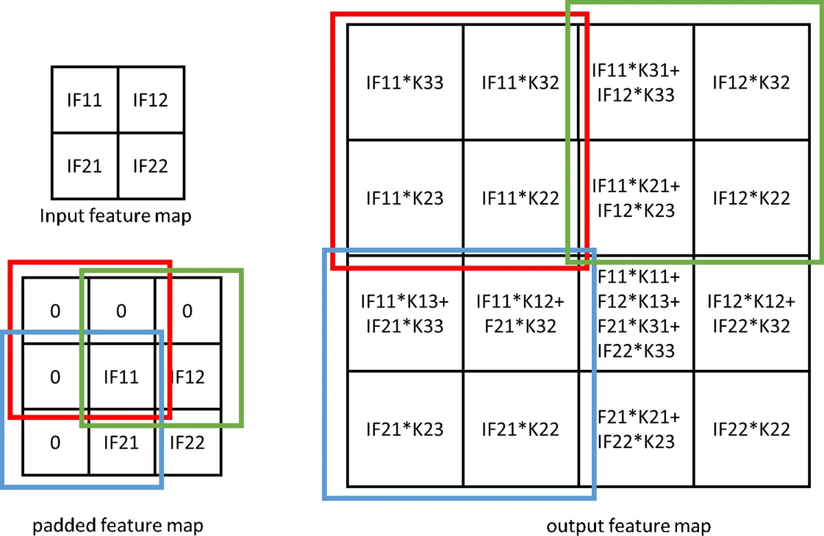
Unified PE Structure – Each PE contains nine multipliers and an adder tree, sufficient for a 3×3 convolution kernel. By re‑routing inputs, the same PE can compute a 2×2 deconvolution patch using the same nine multipliers, producing four output pixels in parallel. This eliminates redundant zero‑multiplications that arise when naïvely implementing deconvolution as padded convolution.
-
Loop Optimizations – The authors analyze the four nested loops typical of convolution (output channel, input channel, output spatial dimension, kernel spatial dimension). They fully unroll the outermost loop (output channels), partially unroll the input‑channel loop to balance DSP usage, and fully unroll the pixel‑reuse loop. Loop tiling is applied on the depth dimension to fit on‑chip BRAM, and loop interchange is used to maximize data locality. These choices reduce the number of partial sums that must be written to external DRAM, thereby lowering memory bandwidth requirements.
-
Line‑Buffer and Shift‑Register Design – A configurable line buffer sits between the AXI‑DMA interface and the input‑feature‑map (IF) buffer. It supports multiple padding modes and dynamically generates the required sliding windows for both 3×3 convolution and 2×2 deconvolution. The IF buffer stores data as 3×1 vectors, which are expanded into the appropriate window by a shift register before reaching the PE array.
-
Integrated Batch‑Normalization and Activation – During inference, batch‑normalization parameters are folded into a single multiplication‑addition pair and absorbed into the PE datapath. The accelerator supports ReLU and LeakyReLU without extra hardware stages.
-
Scalable Architecture – The number of PE arrays can be scaled according to the target FPGA’s DSP count and memory bandwidth. In the presented implementation, a single PE array (64‑bit data width) is used, but the design permits replication to achieve higher throughput.
The authors implement the architecture on a Xilinx ZC706 board (Zynq‑7000 series) targeting SegNet‑Basic, which consists of four encoder convolutions, three max‑poolings, two decoder convolutions, and three decoder deconvolutions. The network parameters occupy ~42 MB; 8‑bit fixed‑point quantization is applied to both weights and activations. Using Simulink and the HDL Coder toolbox, the design is synthesized at 220 MHz. Resource utilization is 16,579 LUTs (8 % of the device), 25,390 registers (6 %), 537 BRAM blocks (99 % of on‑chip memory), and 576 DSP slices (64 %).
Performance results show 151.5 GOPS for convolution and 94.3 GOPS for deconvolution, surpassing prior FPGA implementations that either lack deconvolution support or achieve lower throughput. The unified design incurs a modest penalty in pure convolution speed compared with highly specialized convolution accelerators, but the overall balance between convolution and deconvolution performance, together with the reduced hardware footprint, is highlighted as a key advantage.
Latency measurements on a 90 × 120 feature map indicate that convolution and deconvolution take comparable time; the additional padding overhead for deconvolution is only ~0.6 µs, and the combined pooling and ReLU adds ~1.2 µs. Double buffering eliminates data‑transfer differences, resulting in a net 3.2 % processing‑time saving when using deconvolution instead of a convolution‑plus‑pooling‑plus‑ReLU sequence.
The paper concludes that a unified PE‑based accelerator can efficiently support both operations without extra circuitry, simplifying design and improving resource efficiency for segmentation networks. Future work is suggested in scaling to larger networks, exploring power‑aware optimizations, and integrating the architecture into automated design toolchains.
Comments & Academic Discussion
Loading comments...
Leave a Comment