Unsupervised Competitive Hardware Learning Rule for Spintronic Clustering Architecture
We propose a hardware learning rule for unsupervised clustering within a novel spintronic computing architecture. The proposed approach leverages the three-terminal structure of domain-wall magnetic tunnel junction devices to establish a feedback loop that serves to train such devices when they are used as synapses in a neuromorphic computing architecture.
💡 Research Summary
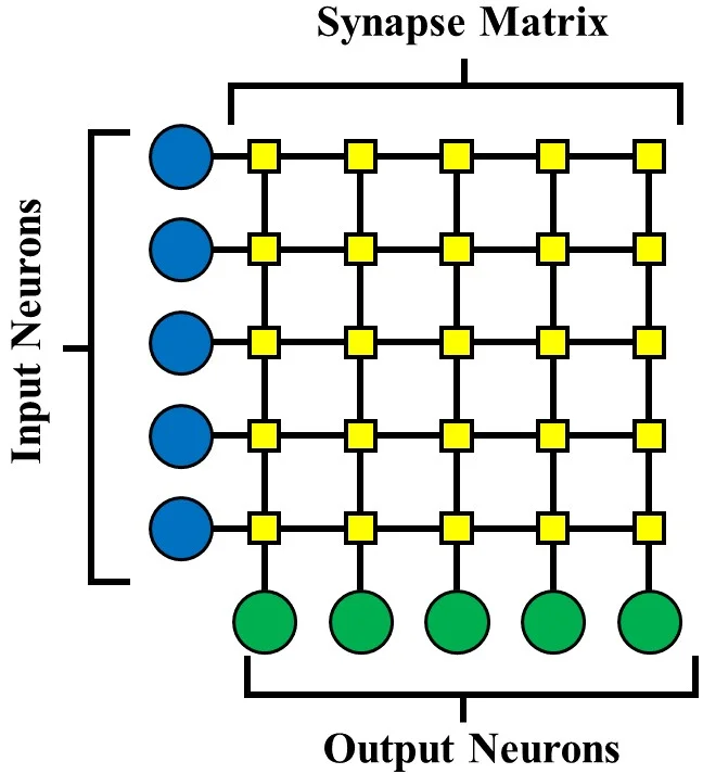
The paper presents a novel hardware learning rule for unsupervised clustering implemented within a spintronic neuromorphic architecture. The core of the proposal is the exploitation of three‑terminal domain‑wall magnetic tunnel junction (3T DW‑MTJ) devices as analog synapses and four‑terminal DW‑MTJ devices as leaky‑integrate‑and‑fire (LIF) neurons. By interconnecting these devices in a cross‑bar array, the authors create a feedback loop in which the output of a neuron directly drives a current back into the synapses that contributed to its firing. This feedback current, whose direction depends on the input pixel polarity, moves the domain wall in the synapse’s magnetic track, thereby increasing or decreasing the MTJ conductance (i.e., the synaptic weight). The mechanism implements a Hebbian‑type learning rule that is electrically equivalent to spike‑timing‑dependent plasticity (STDP) but without the need for peripheral digital control logic.
The paper first motivates neuromorphic computing as a path toward energy‑efficient AI, noting that conventional CMOS synapses lack non‑volatility and incur high static power. Spintronic domain‑wall devices, by contrast, offer non‑volatile analog storage, ultra‑low write energy, and fast switching. The three‑terminal synapse separates the write path (S2‑S1) that moves the domain wall from the read path (S1‑S3) that participates in the vector‑matrix multiplication. The four‑terminal neuron integrates input currents through its N1‑N2 write path, while the N3‑N4 read path provides a binary conductance that determines whether the neuron fires. Leakage is realized either by a magnetic coupling field, an anisotropy gradient, or shape‑induced drift, ensuring that the domain wall naturally relaxes unless reinforced by input.
A detailed circuit description follows. During inference, input pixels are encoded as either ground (0) or Vdd (1) voltages applied to the S1 terminals of the synapses. The feed‑forward current IFF travels through S1‑S3‑N1‑N2, is modulated by the analog synaptic conductance, and charges the neuron’s integration node. When the neuron’s internal domain wall crosses a threshold, the binary MTJ in the N3‑N4 path switches to a low‑resistance state, producing a spike that propagates to downstream layers. Simultaneously, a feedback path connects the neuron’s N4 terminal to the S2 terminal of each synapse that feeds that neuron. The feedback current IFB flows through N3‑N4‑S2‑S1; its polarity is set by the pixel voltage at the neuron’s input. Positive IFB (pixel = ground) moves the domain wall in a direction that reduces conductance, while negative IFB (pixel = Vdd) increases conductance. The binary MTJ between N3‑N4 controls the magnitude of IFB, thus modulating the learning rate: a firing neuron presents a high conductance, delivering a strong learning signal; a non‑firing neuron presents a low conductance, delivering a weak signal.
Mathematically, the synaptic conductance Gs(t) is expressed as a linear interpolation between the anti‑parallel (GAP) and parallel (GP) MTJ conductances based on the domain‑wall position xs(t) and tunnel‑barrier width ws. Normalizing Gs yields a weight ω(t) ∈
Comments & Academic Discussion
Loading comments...
Leave a Comment