Towards Substrate Engineering of Graphene-Silicon Schottky Diode Photodetectors
Graphene-Silicon Schottky diode photodetectors possess beneficial properties such as high responsivities and detectivities, broad spectral wavelength operation and high operating speeds. Various routes and architectures have been employed in the past to fabricate devices. Devices are commonly based on the removal of the silicon-oxide layer on the surface of silicon by wet-etching before deposition of graphene on top of silicon to form the graphene-silicon Schottky junction. In this work, we systematically investigate the influence of the interfacial oxide layer, the fabrication technique employed and the silicon substrate on the light detection capabilities of graphene-silicon Schottky diode photodetectors. The properties of devices are investigated over a broad wavelength range from near-UV to short-/mid-infrared radiation, radiation intensities covering over five orders of magnitude as well as the suitability of devices for high speed operation. Results show that the interfacial layer, depending on the required application, is in fact beneficial to enhance the photodetection properties of such devices. Further, we demonstrate the influence of the silicon substrate on the spectral response and operating speed. Fabricated devices operate over a broad spectral wavelength range from the near-UV to the short-/mid-infrared (thermal) wavelength regime, exhibit high photovoltage responses approaching 10$^6$ V/W and short rise- and fall-times of tens of nanoseconds.
💡 Research Summary
This paper investigates how the interfacial oxide layer and the silicon substrate affect the performance of graphene‑silicon (G‑Si) Schottky diode photodetectors. Two device architectures were fabricated on identical n‑type silicon wafers (ρ = 1–10 Ω·cm, N_d ≈ 3.5 × 10¹⁴ cm⁻³): (i) a graphene/insulator/silicon (GIS) structure that retains the native SiO₂ (~2 nm) and (ii) a graphene/silicon (GS) structure where the oxide is removed by a brief HF dip before graphene transfer. Both devices share a large lateral junction area (~60 mm²) and a 800 nm photoresist spacer that serves as an insulating support for the metal contacts (Au/Cr on graphene, Al on the silicon backside).
Electrical characterization shows that the GIS device exhibits a higher on/off current ratio (≈10⁵) than the GS device (≈10⁴). Temperature‑dependent I‑V measurements yield Schottky barrier heights (SBH) of 0.62 eV for GIS and 0.45 eV for GS, while built‑in potentials derived from C‑V are 0.58 V and 0.31 V, respectively. The presence of the thin oxide in GIS acts as a tunneling barrier, suppressing low‑bias current and thereby improving the signal‑to‑noise ratio. Over five weeks of ambient storage, the GS device’s SBH rises to 0.61 eV and its on/off ratio increases, indicating that oxygen and water diffuse through graphene defects and regrow a native oxide under the graphene. The GIS device shows only modest changes, consistent with its initially self‑limited oxide thickness.
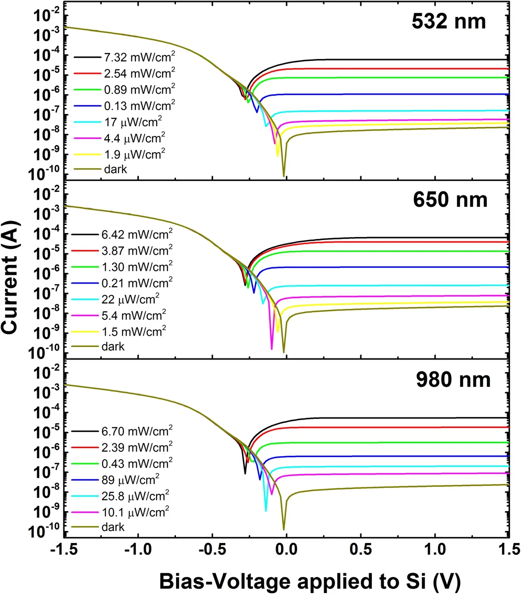
Optical testing was performed with continuous‑wave lasers at 532 nm, 650 nm, and 980 nm, as well as with broadband white light filtered by a monochromator. For wavelengths below the silicon bandgap (λ < 1.1 µm), silicon dominates absorption; a large SBH is beneficial because it reduces reverse dark current, leading to high photovoltage. For longer wavelengths (λ > 1.1 µm), graphene absorbs the photons, and a lower SBH (as in the GS device) facilitates carrier transmission over the barrier, improving photocurrent. Under illumination, the open‑circuit voltage (V_oc) shifts toward forward bias as light intensity increases, while the reverse‑bias current saturates sharply, independent of intensity.
A theoretical model separates drift (J_dr) and diffusion (J_diff) contributions to the total photocurrent (J_tot = J_dr + J_diff). The depletion width x_d is calculated from the built‑in potential, applied reverse bias, and doping concentration. Light absorption follows Beer‑Lambert law, yielding a depth‑dependent generation rate G_e,h. Drift current is proportional to the fraction of light absorbed within the depletion region, whereas diffusion current depends on the hole diffusion length L_p, recombination velocity S_p at the back surface, and substrate thickness H. Using a hole mobility μ_p = 400 cm² V⁻¹ s⁻¹ and a recombination time τ_p = 2 × 10⁻⁴ s, the diffusion length is on the order of hundreds of micrometers, comparable to the 500 µm silicon wafer thickness. Consequently, for long‑wavelength light (low absorption coefficient α) a substantial portion of carriers is generated deep in the substrate, and diffusion contributes significantly to the responsivity.
Calculated responsivity curves as a function of depletion length show that increasing x_d enhances drift‑dominated response (fast, high‑gain) for short wavelengths, while longer x_d boosts diffusion‑dominated response for mid‑ and long‑infrared wavelengths. This explains the experimental observation that GIS devices, with a higher SBH and thus larger built‑in field, deliver higher photovoltage in the visible/NIR, whereas GS devices excel in the infrared regime.
High‑speed measurements reveal rise and fall times on the order of tens of nanoseconds, far faster than the carrier recombination time, thanks to graphene’s high carrier mobility and the vertical electric field across the depletion region.
In summary, the study demonstrates that (1) a thin interfacial oxide can be advantageous for improving on/off ratios and photovoltage in the visible range, (2) the silicon substrate’s doping level and thickness critically shape the balance between drift and diffusion currents, thereby dictating spectral response and speed, and (3) careful engineering of both interface and substrate enables graphene‑silicon Schottky photodetectors that operate from near‑UV to mid‑infrared, achieve photovoltage responsivities approaching 10⁶ V/W, and maintain nanosecond‑scale response times, positioning them as promising candidates for broadband, high‑speed optoelectronic applications.
Comments & Academic Discussion
Loading comments...
Leave a Comment