Experimental Demonstration of Probabilistic Spin Logic by Magnetic Tunnel Junctions
The recently proposed probabilistic spin logic presents promising solutions to novel computing applications. Multiple cases of implementations, including invertible logic gate, have been studied numerically by simulations. Here we report an experimental demonstration of a magnetic tunnel junction-based hardware implementation of probabilistic spin logic.
💡 Research Summary
The paper presents an experimental demonstration of Probabilistic Spin Logic (PSL) using magnetic tunnel junctions (MTJs) as the fundamental stochastic units, termed “p‑bits.” Building on prior work that generated random signals from thermally stable MTJs, the authors introduce a new operation scheme that simultaneously applies a constant bias voltage and a static magnetic field to each MTJ. By adjusting the voltage and field independently, the average dwell times of the parallel (P) and anti‑parallel (AP) magnetic states can be tuned, allowing the stochastic output of each p‑bit to be biased by an external input while preserving its intrinsic randomness.
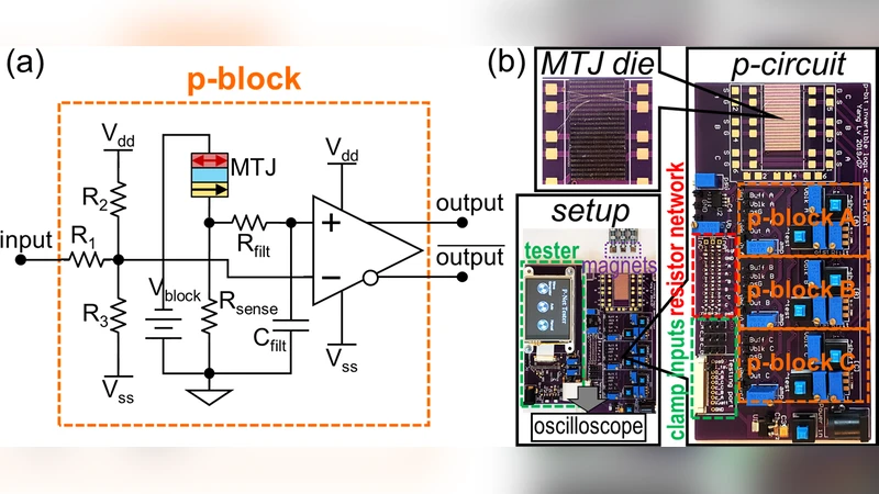
A basic building block, called the p‑block, is designed to convert the random switching of an MTJ into a usable digital signal. The input voltage is attenuated and shifted through a resistor network (R1‑R3) and fed to a comparator as a threshold. The MTJ is driven by a DC source through a small sense resistor (Rsense), which converts the MTJ’s resistance fluctuations into a voltage Vmtj. A low‑pass filter (Rfilt‑Cfilt) smooths Vmtj before it reaches the comparator, shaping the transfer characteristic of the p‑block. Experimental results show that without filtering the Vmtj waveform swings sharply between the supply rails, producing a step‑like transfer curve. Increasing the filter time constant progressively smooths the waveform, narrows the voltage distribution, and transforms the transfer curve from a binary step to a sigmoidal shape, which is desirable for probabilistic computing.
The response time of the p‑block is measured by applying a step input and overlaying 100 captured output waveforms. The earliest observable transition occurs in less than 1 µs, limited by the input driver’s slew rate rather than the MTJ itself. The intrinsic switching frequency of the MTJ is on the order of 1 MHz, suggesting that the p‑bit can operate at sub‑microsecond timescales.
Using three identical p‑blocks, the authors construct a probabilistic circuit (p‑circuit) that implements an invertible AND gate. Each p‑bit can be externally “clamped” to logic 0, logic 1, or left floating via dedicated clamp lines (RcA, RcB, RcC). The three p‑bits are interconnected through a resistor network that enforces the logical constraint C = A·B. When A and B are clamped, C fluctuates around the expected logical value; when C is clamped, the allowed combinations of A and B collapse to those satisfying the constraint. The authors demonstrate forward operation (input‑to‑output), backward operation (output‑to‑input), and free‑run operation (all bits floating). Histograms of the joint states
Comments & Academic Discussion
Loading comments...
Leave a Comment