A Single-MOSFET MAC for Confidence and Resolution (CORE) Driven Machine Learning Classification
Mixed-signal machine-learning classification has recently been demonstrated as an efficient alternative for classification with power expensive digital circuits. In this paper, a high-COnfidence high-REsolution (CORE) mixed-signal classifier is propo…
Authors: Farid Kenarangi, Inna Partin-Vaisb
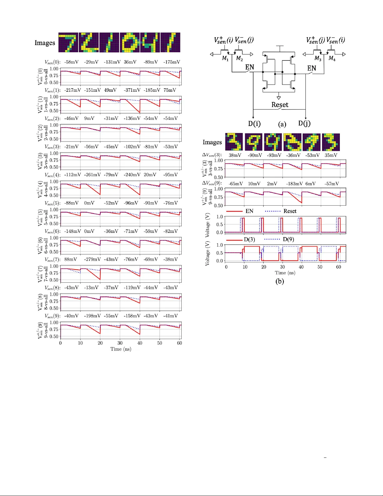
1 A Single-MOSFET MA C for Confidence and Resolution (CORE) Dri v en Machine Learning Classification Farid K enarangi, Student Member , IEEE and Inna Partin-V aisband, Member , IEEE Abstract —Mixed-signal machine-learning classification has r e- cently been demonstrated as an efficient alternativ e for classifica- tion with power expensiv e digital circuits. In this paper , a high- COnfidence high-REsolution (CORE) mixed-signal classifier is proposed for classifying high-dimensional input data into multi- class output space with less power and area than state-of-the-art classifiers. A high-r esolution multiplication is facilitated within a single-MOSFET by feeding the features and feature weights into, respecti vely , the body and gate inputs. High-resolution classifier that considers the confidence of the individual pr edictors is designed at 45 nm technology node and operates at 100 MHz in subthreshold r egion. T o ev aluate the performance of the classifier , a reduced MNIST dataset is generated by downsampling the MNIST digit images fr om 28 × 28 features to 9 × 9 features. The system is simulated across a wide range of PVT variations, exhibiting nominal accuracy of 90%, energy consumption of 6.2 pJ per classification (over 45 times lower than state-of-the-art classifiers), area of 2,179 µ m 2 (over 7.3 times lower than state-of- the-art classifiers), and a stable response under PVT variations. Index T erms —machine lear ning hard ware, mixed-signal clas- sifiers, confidence-level, high resolution, high-dimensional data, multi-class classification, linear classifiers, logistic regr ession, subthreshold. I . I N T R O D U C T I O N L OW power machine learning (ML) classifiers are playing an important role in enabling edge computation of ML algorithms. W ide variety of applications benefit from these compact classifiers, such as, Internet of Things (IoT) de vices, wireless sensor networks (WSNs), smart home technologies, autonomous transportation, and security systems. Existing on-chip classifiers can be categorized into two major domains: digital and mixed-signal [1]. A digital clas- sifier is typically fed with binary inputs ( i.e. , features) and uses binary feature weights, all obtained by sampling and quantizing corresponding analog signals. The classification accuracy with digital classifiers increases with the increasing number of bits assigned for features and weights. These highly accurate digital classifiers howe ver exhibit significant power consumption and physical size and are often not suitable for power limited applications, such as battery powered sensors and those other IoT devices that are wirelessly powered and powered from harv ested energy . Alternati vely , mixed signal classifiers aim to reduce the area and po wer consumption of the conv entional digital classifiers by directly using the analog input data for classification [2]. The inherent need for data con version with power hungry analog-to-digital con verters (ADCs) is therefore mitigated with mix ed-signal classifiers [2]. Another concern in modern classifiers is the high dimen- sionality of data. Classifying data in a high-dimensional space The authors are with the Department of Electrical and Computer Engi- neering, University of Illinois at Chicago, Chicago, IL 60607 USA (e-mail: fkenar2@uic.edu; vaisband@uic.edu). Fig. 1. Schematic of the proposed linear binary classifier . Features and feature weights are fed into, respecti vely , the body and gate input of the individual MOS transistors. Separate lines are used for positiv e and negativ e weights. often results in a prohibiti vely high data movement among memory and computing circuit components. This, in turn, significantly increases power consumption in both, mixed- signal and digital classifiers [3]–[15]. T o reduce the data mov ement, several approaches for in-memory ML computa- tion have recently been proposed. Recent state-of-the-art in- memory classifiers typically exhibit accuracy between 90% and 96% and energy dissipation in the range of 210 pJ/decision to 879 pJ/decision [16]–[19] for typical image recognition datasets. Emerging de vice technologies are also being con- sidered for providing power and area ef ficient alternatives for the con ventional CMOS based classifiers. Accuracy of 90% and energy of 25 pJ per decision has been recently reported in [20], [21]. T o enable high-resolution feature-weight multiplication, a theoretical framework that comprises circuits, models, and algorithms is proposed. T o the best of the authors knowledge, this paper is the first to report a mixed-signal high-resolution classifier , utilizing MOSFET body terminals. The schematic of the proposed configuration is shown in Fig. 1. W ith this approach, body bias of the MOSFETs is controlled by the individual ML features, the gate inputs are fed by the absolute value of a corresponding feature weight, and the sign of the weights is taken into account by considering separate lines for the positiv e and negati ve feature and feature weight product. A K -class classification with N features is therefore realized with N rows and K columns multiplication and accumulation (MA C) array , where each column serves as an independent 2 binary classifier . These individual binary classifiers are com- bined using one-versus-all technique [22], requiring 1 2 ( K − 1) times less binary classifiers than the state-of-the-art classifier in [16] and orders of magnitude less transistors, as compared with other existing mixed-signal classifiers [17], [19]. Another primary contribution is in decision making domain. W ith analog classifiers, binary predictions are typically made based on the relati ve magnitude of signals between the positi ve and negativ e sensing lines. W ith this traditional approach, the sensing line with the highest voltage drop is assumed to exhibit the correct classification and the confidence le vel of the decision is not considered. Alternati vely , a small dif ference in these voltage drop values indicates low confidence le vel of the individual binary predictions and thus, a higher probability of an erroneous final decision. T o address this ML integrity issue, a confidence driv en classification is proposed in this paper . W ith this approach, the difference among the magnitudes of the sensing line voltage drops is considered for capturing the confidence of the individual predictions. Finally , the proposed system is designed in subthreshold re- gion, e xhibiting a po wer efficient alternative for the traditional classifiers. The classifier is demonstrated on Modified National Institute of Standards and T echnology (MNIST) dataset [23] of 10-class digit images. Based on SPICE circuit le vel simulation results, MNIST data is classified with 90% accuracy using 81 × 10 transistors and exhibits power consumption of only 6.2 pJ per decision. The rest of the paper is organized as follo ws. In Section II, the proposed high-resolution binary classifier and linearization technique are described. Fabrication considerations are also discussed in this section. Based on the proposed binary clas- sifier , a multi-class high-resolution classifier is designed and demonstrated with MNIST dataset, as described in Section III. Confidence driven classification is also explained in Section III. Circuit design and simulation results of the multi-class high-COnfidence high-REsolution (CORE) classifier using one-versus-all technique are presented in Section IV. The paper is summarized in Section V. I I . T H E P RO P O S E D L I N E A R B I NA RY C L A S S I F I E R In this section, the proposed linear binary classifier is described. The software lev el design frame work is provided in Section II-A. The circuit, and fabrication lev el considerations are presented in, respectively , Sections II-B and II-C. A. Design F ramework Reliability , power consumption, and physical size of on- chip classifiers are all primary concerns in modern ML ICs. The proposed framework is designed to meet accuracy speci- fications of modern classification problems in a cost effecti ve manner . Linear algorithms are exploited in this paper for training a supervised binary classifier , optimizing the system for linearly separable input data. Fig. 2. Handwritten digits from MNIST dataset, (a) original image (default resolution with 28 × 28 features), (b) selected features shown with light squares, and (c) downsampled image with 9 × 9 features. W ith a multiv ariate linear classifier , the system response Z is a linear combination of N input features x = ( x 1 , x 2 , ..., x N ) and model weights w = ( w 1 , w 2 , ..., w N ) , Z = N X i =1 w i · x i , Z ∈ R . (1) The model weights are determined during supervised training by minimizing the prediction error between the system re- sponse, Z , and a corresponding true v alue in the labeled train- ing dataset. Logistic regression (LR) – a common supervised linear ML model – is used for training the proposed classifier based on gradient descent algorithm [24]. LR is preferred due to its simple implementation and superior performance on MNIST dataset as compared with other classifiers. In inference, a probability threshold of 0 . 5 is used for predicting system response to input data, exhibiting a simple on-chip implementation, ˆ y = sign ( Z ) = sign ( P N i =1 w i · x i ) = 1 , Z ≥ 0 − 1 , Z < 0 . (2) The described logistic regressor with the probability threshold of 0.5 is referred to as logistic classifier . The accuracy of the proposed logistic classifier is e valuated as a percentage of all the correct predictions out of the total number of test predictions. The proposed ML flow and the preprocessing steps are explained below . 1) Dataset: MNIST database is a large image dataset, com- monly used for ev aluating the effecti veness of ML hardware. MNIST contains images of 70,000 handwritten digits, ranging between 0 to 9. Each digit comprises 784 ( 28 × 28 ) image pixels. The training and test datasets comprise, respectiv ely , 60,000 and 10,000 digits. Out of the 60,000 training obser- vations, 45,000 and 15,000 digits are used for , respectively , training and v alidating the proposed system. 2) F eatur e selection and downsampling: Each image pixel of the individual digits in the training set is considered as an ML feature and used for training the classifier . T o reduce the power and area overheads, those redundant features that are not essential for digit classification are eliminated. T o deter- mine the preferred number of observed features, the dataset is downsampled to N ≤ 784 features ( N = 6 2 , 7 2 , . . . . 28 2 ) and classification accuracy is obtained for the downsampled data in Python. T o ef ficiently classify MNIST digits with the proposed classifier , N = 81 (9 × 9) is preferred, corresponding to 90% accuracy . The original and downsampled ( N = 81 ) digit images are shown in Fig. 2. 3 B. Cir cuit Level Considerations The primary goal in a linear binary classification is to accurately and efficiently perform the dot product operation of the features and feature weights, as described in (2). T o simplify the circuit lev el design, the result sho wn in (2) is formulated as the signed addition of positiv e, Z + , and negati ve, Z − , feature-weight products, ˆ y = sign ( Z + z }| { X w i > 0 x i · w i + Z − z }| { X w j < 0 x j · w j ) = 1 , Z + ≥ Z − − 1 , Z + < Z − . (3) The individual positiv e and negati ve feature-weight prod- ucts are accumulated within the positive, V + sen and negati ve V − sen sensing lines, yielding the basic ML multiplication and accumulation (MAC) operation, as sho wn in Fig. 1. For each feature-weight multiplication, a single-MOSFET is connected to either the positive or ne gative sensing line, as determined by the sign of the corresponding feature weight. For example, for w 1 < 0 , the corresponding multiplier MOSFET is connected to the negati ve sensing line. T o capture the v oltage drops across the sensing lines, sensing capacitors ( i.e. , C sen ) are connected to the indi vidual sensing lines. The size of a sensing capacitor is determined proportionally to sensing line current, increasing with the number of transistors ( i.e. , features) connected to the line. T o classify tasks with higher number of features, larger sensing capacitors are therefore required, limiting the scalability of the system. T o provide a power efficient and scalable solution, the transistors are biased in near/subthreshold operation region, significantly limiting the current through the sensing lines. In the case of MNIST classification with 9 × 9 features, capacitance of only 50 fF is utilized per sensing line. A primary concern with near/subthreshold operation is the exponential dependence of the drain current on the body and gate biases [25], I sub = W L I t exp ( V g s − V th nV T )[1 − exp ( − V DS V T )] , (4) where I t is the sub-threshold current at V g s = V th , n is the sub-threshold slope, and V T is the thermal v oltage. Note that body v oltage dependence is embedded in the threshold v oltage, V th ∝ √ V bs . Considering that V DS >> V T , the expression in (4) can be simplified as, I sub = W L I t exp ( V g s − V th nV T ) , V DS >> V T . (5) T o mitigate the non-linear dependence of the drain current on the weight-feature dot product (see (1)), a novel training flow is proposed (see Fig. 3). T o account for the non-linear dependence of the drain current on the bias voltage, the model is trained with square root values of the default features ( x i → √ x i ) ). Thus, the extracted feature weights, w , are optimized for classifying the MNIST dataset transformed into half-order polynomial space. Alternatively , to account for the non-linear dependence of the drain current on the gate voltage, the feature weights are logarithmically adjusted ( w i → ln( w i ) ), exhibiting V g s ∝ ln( w ) . Using the first-order approximation of exp( √ V bs ) ≈ 1 + √ V bs , the current in this Fig. 3. Linearization flow . T o account for the non-linear dependence of the drain current on the body bias, I sub ∝ √ V bs , the model is trained to make predictions based on the square root values of the original features. The optimized weights are logarithmically adjusted, mitigating the exponential dependence of the subthreshold current on the gate bias. case is expressed as, I sub ∝ exp(ln( V g s )) · exp( p V bs ) ∝ V g s · p V bs ∝ w · √ x. (6) In inference, the current model is exploited for making predic- tion based on the square root v alues of the original features, as trained offline, yielding 90% accuracy across the MNIST test set, as detailed in the follo wing sections. 4 C. F abrication Costs In the proposed linear binary classifier, the body and gate terminals are fed by , respectively , the input features and corresponding feature weights. Each multiplication is, there- fore, executed by a single-MOSFET , significantly reducing the power and area costs (despite the o verhead of the triple- well technology) and complexity (as determined by number of transistors) of the classifier in comparison to the existing state-of-the-art mixed-signal classifiers [2], [16]. Con ventional twin-well fabrication process is illustrated in Fig. 4(a). This process is designed to provide a single voltage connection to all the n-type and p-type body terminals. Alter- nativ ely , to connect body terminals of the indi vidual multiplier transistors to different voltage le vels, a specialized fabrication process is required. One way to indi vidually bias numerous body terminals, is by fabricating with triple-well process (see Fig. 4(b)), which is commonly used in high-performance, low-po wer ICs [26], [27] and for reducing substrate noise in mixed-signal circuits [28]. In a p-substrate triple-well process, an additional deep n-well is used to isolate the p-well of each MOSFET from the p-substrate, allo wing an independent body terminal connection for each MOSFET . The triple-well structure has been demonstrated to provide better noise char- acteristics as compared with the traditional twin-well structure, without increasing the gate leakage [29]. Alternativ ely , the triple-well structure, exhibits additional fabrication costs and area ov erheads that needs to be considered. Layout of a four- transistor block in twin-well and triple-well process is shown in, respectiv ely , Fig. 4(c) and Fig. 4(d). W ith the triple-well configuration, the area is increased 3 times as compared with the twin-well process in 45 nm CMOS technology . I I I . C O R E BA S E D M U L T I - C L A S S C L A S S I F I E R A multi-class classifier is designed based on multiple lin- ear binary classifiers, as presented in Section II. Confidence driv en approach that addresses the integrity of multi-class classification is described in Section III.A. The transistor lev el implementation of the proposed CORE classifier is presented in Section III.B. A. Confidence Driven Classification: O VO versus O V A T wo typical approaches for designing a multi-class classifier based on multiple binary classifiers are one-versus-one (O VO) and one-versus-all (O V A) [30]. With O VO approach, all pair- wise combinations of the output classes are e valuated with the individual binary classifiers. Thus, a K -class classification with O V O approach requires 1 2 K ( K − 1) binary classifiers, increasing the system complexity and power and area costs quadratically with the number of classes. For example, for classifying 10 digits with O V O approach, 45 i -verus- j , ( i, j ∈ { 0 , 1 , 2 , .., 9 } ) binary classifiers are required. Alternatively , in case of a 1,000 class classification, about half a million of binary classifiers are required. The final decision with O V O technique is extracted using majority voting approach [31]: each binary classifier v otes independently for a certain class and the final decision is made based on the class with highest number of votes. Fig. 4. T wo commonly used fabrication processes, (a) twin-well process, and (b) triple-well process with p-substrate. Layout of four transistors with W = 200 nm and L = 50 nm in the (c) twin-well, and (d) triple-well configurations. Alternativ ely , with O V A approach, each binary classifier discriminates between a single class and the rest of the classes. The required number of binary classifiers with O V A increases linearly with the number of classes, facilitating a more power and area efficient classification of high-dimensional data. In addition, a probability score of correct discrimination is in- herently provided with O V A and can be extracted for the individual binary classifiers. Thus, a K -class O V A classifier can be designed with as few as K binary classifiers, seam- lessly accounting for the confidence lev el of the individual predictions. The confidence driv en decision, d , with the O V A classifier is determined as, d = i | p i = max ( p i ) , i = 0 , 1 , ..., K − 1 , (7) where p i is the confidence level of the i th binary classifier . From circuit level perspecti ve, the confidence lev el with O V A approach can be determined as the difference of the voltage drops across the positiv e and negati ve sensing lines, e.g . , p i ∝ ∆ V + sen ( i ) − ∆ V − sen ( i ) , ∆ V sen ( i ) . d = i | (∆ V sen ( i )) = K − 1 max j =0 { (∆ V sen ( j ) } . (8) T o extract the class with highest confidence lev el, a light- weight comparator is designed, as described in the next subsection, yielding a po wer and area efficient alternativ e for the traditional voter circuits. B. Cir cuit Level Design and Simulation Results The proposed multi-class classifier is designed in SPICE and demonstrated based on the reduced MNIST dataset. The O V A 5 Fig. 5. V oltage wav eforms of the sensing lines during the precharge ( i.e. , ( 0 − 2 . 5 ns ), ( 10 − 12 . 5 ns ), ( 20 − 22 . 5 ns ), ( 30 − 32 . 5 ns ), ( 40 − 42 . 5 ns ), and ( 50 − 52 . 5 ns ) ) and classification stages ( i.e. , ( 2 . 5 ns − 10 ns ), ( 12 . 5 ns − 20 ns ), ( 22 . 5 ns − 30 ns ), ( 32 . 5 ns − 40 ns ), ( 42 . 5 ns − 50 ns ), and ( 52 . 5 ns − 60 ns ) for six consecutive input features ( i.e. , 7, 2, 1, 0, 4, and 1). circuits and architecture of the MOSFET array are described in this section. 1) MA C Array: T o classify the do wnsampled 9 × 9 MNIST digits, ten binary classifiers (see Section II) are co-designed in SPICE, yielding a 81 × 10 MOSFET array . Each of the transistors within the MA C array is exploited for generating a single feature-weight product. During inference, the V + sen and V − sen lines are precharged to V DD prior to each prediction. Fig. 6. Schematic of the proposed confidence level extractor . The confidence le vel of the i th and j th binary classifiers is extracted and the prediction of the most confident classifier is used as the final decision. All the input features and feature weights are connected simultaneously to, respectiv ely , the body and gate terminals of the indi vidual multiplier transistors, facilitating a parallel classification process within all the ten binary classifiers. As a result, 20 different voltage drop v alues ( i.e . , V + sen ( i ) , V − sen ( i ) , i = 0 , 1 , . . . , 9 ) are generated on the individual sensing lines, as sho wn in Fig. 5. The voltage waveforms of the positi ve and negati ve sensing lines are illustrated by , respectiv ely , the blue dotted and solid red lines. These voltage drops are exploited by the confidence level extractor , generating the final classifier decision. The confidence le vel of each binary classifier (as determined based on (8)) is sho wn in Fig. 5, as noted on top of each plot. For e xample, for digit 7, the 7 th (7-vs-all) binary classifier has as expected the highest confidence lev el. The final decision is generated by the confidence level extractor . 2) Confidence Level Extractor: The schematic of a single confidence driven selector for a multi-class classification is presented in Fig. 6(a). For a K -class classification, 1 2 K ( K − 1) confidence driv en selectors are required, yielding a total of 6 Fig. 7. Schematic of the resistive voltage divider . No sensitivity to process variations is observed with 1K-run Monte-Carlo simulation. Fig. 8. Schematic of the proposed classifier, comprising voltage divider , MOSFET array , and confidence lev el extractors. 45 selectors for the MNIST dataset ( K = 10 ). The circuit is designed to compare the confidence le vels of the binary classifiers ( i th and j th classifier) and determine the classifier with higher confidence level, ∆ V + sen ( i ) − ∆ V − sen ( i ) <> ∆ V + sen ( j ) − ∆ V − sen ( j ) . (9) T o simplify the circuit le vel implementation the subtraction in (9) is replaced with summation, ∆ V + sen ( i ) + ∆ V − sen ( j ) <> ∆ V + sen ( j ) + ∆ V − sen ( i ) . (10) Each summation in (10) is captured with two parallel NMOS transistors, as sho wn in Fig. 6(a). T o capture the result of ∆ V + sen ( i ) + ∆ V − sen ( j ) , the gate terminals of the transistors M 1 and M 2 are connected to, respectiv ely , the positive sensing line of the i th classifier , V + sen ( i ) , and negati ve sensing line of the j th classifier , V − sen ( j ) . As a result, the drain current at M 1 and M 2 is proportional to ∆ V + sen ( i ) + ∆ V − sen ( j ) . Similarly , the gate terminals of the transistors M 3 and M 4 are connected to, respectiv ely , V + sen ( j ) and V − sen ( i ) , generating a drain current proportional to ∆ V + sen ( j ) + ∆ V − sen ( i ) . T o determine which side exhibits higher confidence lev el ( i.e. , sinks lower current), two back to back in verters are utilized. V oltage wav eforms of the sensing lines, EN signal which enables the back-to-back in verters, Reset signal which resets the voltages stored on both sides of the back-to-back in verters and output signals are illustrated in Fig. 6(b) for six consecutiv e classification periods. During the second, third, and fifth classifications, the left side of the in verters sink higher current than the right side. The left and right sides of the confidence selector, are, therefore, forced to, respectively , the low ( i.e. , D ( i ) = 0) and high ( i.e. , D ( j ) = 1) output voltage. Alternativ ely , during the first, fourth, and sixth classifications, the right side sinks higher current than the left side. Thus, left and right sides are forced to, respecti vely , the high ( i.e. , D ( i ) = 1) and low ( D ( j ) = 0) output v oltage. The correct functionality of the confidence lev el extractor depends on its symmetric structure and is highly sensitiv e to process v ariations. T o mitigate process variations, larger pull-down ( W = 5 W min ), pull-up ( W = 15 W min ), and confidence e xtractor ( W = 5 W min ) transistors are utilized for the confidence le vel extractor . W ith upsized transistors, the av erage accuracy degradation of the classifier is limited to 2% under process variations, as described in the next section. Note that con ventional methods such as extracting final classification results with K analog-to-digital (ADCs) can also be lev eraged, trading-off po wer efficiency for scalability ( i.e. , 1 2 ( K − 1) times less confidence extractors). 3) Resistive V oltage Divider: The trained, quantized feature weights are generated using a resistive voltage divider (see Fig. 7). In this configuration, the preferred voltage range ( V low , V hig h ) is divided into 2 n equal steps, where n is the preferred quantization resolution. The gate bias range ( i.e. , ( 300 mV , 610 mV ) is quantized with 5-bit resolution into 31 equal steps of 10 mV , as illustrated in Fig. 7. Poly resistors with sheet resistance of 7.8 Ω / are utilized. The resilience of the voltage divider to process variations is ev aluated with 1K- run Monte-Carlo simulation. Based on the simulation results, the circuit is highly resilient to process v ariations, exhibiting the average deviation of 0.2 mV from the nominal wight values. The results of the 1K-run Monte-Carlo simulation are also shown in Fig. 7. W ith this topology , no memory and data con version units are required for storing and quantizing the weights. Alternati vely , the weights provided with the voltage divider are not reconfig- urable. Using a 32-to-1 multiplex er and a memory unit ( e.g. , SRAM), the circuit can be updated to provide reconfigurable feature weights [32]. The overall area of the classifier with reconfigurable weights is expected to increase by a factor of 4.2. I V . R E S U LT S A. System Characteristics A schematic of the integrated system is illustrated in Fig. 8, comprising v oltage divider , MOSFET array , and confidence 7 (a) (b) Fig. 9. Confusion matrix of the MNIST classification obtained in (a) Python (90% accuracy), and (b) SPICE (90% accuracy), exhibiting no accuracy degradation in SPICE as compared with Python results. lev el extractors. The proposed CORE classifier is designed at 45 nm technology node with the nominal power supply voltage of 0.9 V and threshold voltage of 0.61 V. The body terminals of the MA C array are biased at voltage lev els between 0.2 V and 0.8 V. The area occupied by the classifier is 2,179 µ m 2 , as estimated based on transistor count in SPICE. The MAC array comprises a total of 81 × 10 = 810 MOSFETs. The reduced, 81-feature MNIST dataset is classified with accuracy of 90% within a single 10 ns clock cycle of the system operation, exhibiting no accuracy degradation as compared with the v alidation accuracy in Python. The confusion matrices obtain based on Python and SPICE simulations are shown in, respectiv ely , Fig. 9(a) and Fig. 9(b), exhibiting equal accuracy of 90%. The ML classifier generates predictions at 100 MHz frequency , exhibiting an average energy consumption of 6.2 pJ per classification of a single digit. T o maintain high prediction accuracy , 5 bits and 6 bits are assigned for quantizing, respec- tiv ely , the feature weights and input features. By increasing the dimensionality of the proposed classifier, lower power and area ov erheads can be traded off for higher prediction accuracy , approaching the theoretical limit of 92% for MNIST classification with linear ML algorithms and O V A decisioning scheme. The existing tradeoffs between dimensionality of the data and the accuracy , po wer, and area overheads are sho wn in Fig. 10. The knee point of N = 81 is selected in this paper to provide satisfactory accuracy results in an power and area efficient manner . B. Simulation Results Performance characteristics are listed in T able I for the proposed system along with the existing state-of-the-art mix ed- signal classifiers [2], [16], [17]. Note the different dataset, MIT -CBCL, used in [17]. Classification accuracy is a strong function of data. The accuracy comparison among [17] and other classifiers in T able I is therefore less valuable, albeit the excellent accuracy demonstrated in [17]. Alternatively , benefiting from the high-resolution multiplications and con- fidence driven predictions, CORE classifier exhibits signifi- cantly less transistor count, and thus lower power consumption and smaller IC area, as compared with the other state-of-the- art classifiers. For fair comparison, current time per decision Fig. 10. Existing tradeoffs between the selected number of features, accuracy and (a) area, and (b) power overheads. T ABLE I: System characteristics of the proposed and other existing mixed-signal ML classifiers. [2] [16] [17] Current work Dataset MNIST MNIST MIT -CBCL MNIST T echnology 130 nm 130 nm 65 nm 45 nm Algorithm Ada-boost Ada-boost SVM LR Accuracy 90% 90% 96% 90% Feature weight resolution 4b 1b 8b 5b Feature resolution 5b 5b 8b 6b Number of features 48 81 256 81 Supply voltage (V) 1.2 1.2 0.675 0.9 Speed (MHz) 1.3 50 32 100 Costs Energy (pJ) 543 633.4 210 6.2 Current time per decision (pA · sec) 452.5 527.8 311.1 6.9 Area ( µ m 2 ) 246,792 133,736 401,300 2,179 Normalized area ( µ m 2 /nm 2 ) 14.6 7.91 94.9 1.07 and the system area normalized by squared form factor are also shown in T able I. The current time per decision with the proposed classifier is approximately 45 times lower as com- pared with other approaches. Similarly , area savings (albeit the triple-well technology) range between × 7.3 and × 89 as compared to other classifiers, as shown in T able I. Note that the operational frequency is scalable and can be adjusted based on the application needs and constrains. T o ev aluate the effect of v oltage and temperature variations on the CORE classifier, the supply v oltage is varied between 0.6 volts and 1.2 volt and the temperature is varied between −30 ◦ C and 125 ◦ C. The effect of process variations on the classifier performance is ev aluated based on a 1K-run Monte- Carlo simulation on a randomly selected 100-observ ation (10 images per digit) balanced test set with nominal accuracy of 90%. Note that a 1K-run Monte-Carlo simulation on the whole test set takes 1 , 000 × 2 . 5 hours on Intel Core i7-7700 CPU. The results of the simulations are sho wn in Fig. 11. The 8 Fig. 11. Classifier performance under PVT variations, (a) under temperature variations at typical process corner, TT , and V DD = 0.9 V, (b) under v oltage v ariations at room temperature, T = 27 ◦ C, and at TT , and (c) process and mismatch variations with T = 27 ◦ C and V DD = 0.9 V . classifier exhibits no sensitivity within wide range of voltage variations from 0.8 V to 1.2 V. Less than 2% accuracy degrada- tion is observed at lo w temperatures − 30 ◦ C ≤ T ≤ 0 ◦ C . No sensitivity to temperature v ariations for 0 ◦ C ≤ T ≤ 125 ◦ C is observed. An av erage of 2% accuracy degradation is exhibited due to process variations, as extracted from the 1K-run Monte- Carlo simulation. Confidence histograms of the correct and incorrect clas- sifications are shown in, respectiv ely , Fig. 12(a) and Fig. 12(b). W ith the proposed confidence dri ven approach, incorrect classifications often exhibit lower confidence as compared with typically confident, correct predictions. The odds of an incorrect classification to be corrected under process variations are therefore high, fav orably affecting the resilience of the system to variations. Based on the simulation results, the accuracy is improved for nearly one-third of the Monte-Carlo runs. V . C O N C L U S I O N Sev eral state-of-the-art mixed-signal classifiers ha ve re- cently been demonstrated for po wer efficient classification. Accurate classification of multi-dimensional data under the tight power and area constraints is the primary objective in Fig. 12. Confidence lev el distribution for (a) correct, and (b) incorrect classifications. modern on-chip classifiers. A novel circuit topology is pro- posed in this paper for high-COnfidence and high-REsolution (CORE) classification. W ith this topology , body terminals of the MOSFETs are exploited to encode input features, enabling the high-resolution classification. T o enhance the ML integrity in multi-class classifiers, O V A technique is exploited for ef ficiently extracting a final decision based on the confidence le vel of the individual predictors. For a K -class classification, ( K − 1) / 2 times fewer binary classifiers are required with the O V A approach as compared with the traditional O VO method [16]. T o further reduce area and power consumption of the O V A-based CORE classifier , a light- weight confidence extractor is designed, generating the final decision based on the confidence level of the individual binary classifiers. T o the best of the authors knowledge, the proposed CORE classifier is the first integrated system to successfully classify MNIST dataset in subthreshold region using a single- MOSFET MA C. Biasing transistors in subthreshold region significantly decreases the leakage and dynamic currents as well as ov erall load on the sensing lines. The proposed CORE classifier is designed in SPICE and simulated in 45 nm standard CMOS process. The performance and functionality of the proposed approach is validated with simulation results, exhibiting 90% classification accuracy with 6.2 pJ energy consumption per prediction across the MNIST dataset. Each prediction is finalized within a single clock cycle of 10 ns. The unique topology of CORE classifier supports the ML integrity under a wide range of PVT v ariations, as well as system scalability across technology nodes. R E F E R E N C E S [1] V . Sze, “Designing hardware for machine learning: The important role played by circuit designers, ” IEEE Solid State Cir cuits Mag. , vol. 9, no. 4, pp. 46–54, Nov 2017. [2] Z. W ang and N. V erma, “A low-energy machine-learning classifier based on clocked comparators for direct inference on analog sensors, ” IEEE T rans. Circuits Syst. I, Re g. P apers , v ol. 64, no. 11, pp. 2954–2965, Jun 2017. 9 [3] Y .-H. Chen et al ., “Eyeriss: An energy-ef ficient reconfigurable accelera- tor for deep con volutional neural networks, ” IEEE J . Solid-State Cir cuits , vol. 52, no. 1, pp. 127–138, Jan 2017. [4] R. Hameed et al ., “Understanding sources of inefficiency in general- purpose chips, ” in Pr oc. Int. Symp. Comput. Ar chit. , vol. 38, no. 3, Jun 2010, pp. 37–47. [5] M. Horowitz, “1.1 computing’ s energy problem (and what we can do about it), ” in IEEE Int. Solid-State Circuits Conf. (ISSCC) Dig. T ech. P apers , Feb 2014, pp. 10–14. [6] P . Whatmough et al ., “A 28nm SoC with a 1.2 GHz 568nJ/prediction sparse deep-neural-network engine with > 0.1 timing error rate tolerance for IoT applications, ” in IEEE Int. Solid-State Cir cuits Conf. (ISSCC) Dig. T ech. P apers , Feb 2017. [7] D. Bankman et al ., “An always-on 3.8 µ J/86% CIF AR-10 mixed-signal binary CNN processor with all memory on chip in 28nm CMOS, ” in IEEE Int. Solid-State Cir cuits Conf. (ISSCC) Dig. T ech. P apers , Feb 2018, pp. 222–224. [8] D. Jeon et al ., “A 23-mW face recognition processor with mostly-read 5T memory in 40-nm CMOS, ” IEEE J. Solid-State Circuits , vol. 52, no. 6, pp. 1628–1642, Feb 2017. [9] S. Bang et al ., “14.7 a 288 µ W programmable deep-learning processor with 270KB on-chip weight storage using non-uniform memory hier- archy for mobile intelligence, ” in IEEE Int. Solid-State Cir cuits Conf. (ISSCC) Dig. T ech. P apers , Feb 2017, pp. 250–251. [10] G. Desoli et al ., “14.1 a 2.9 TOPS/W deep conv olutional neural network SOC in FD-SOI 28nm for intelligent embedded systems, ” in IEEE Int. Solid-State Circuits Conf. (ISSCC) Dig. T ech. P apers , Feb 2017, pp. 238–239. [11] K. Bong et al ., “14.6 A 0.62 mW ultra-low-power conv olutional-neural- network face-recognition processor and a CIS integrated with always-on haar-like face detector, ” in IEEE Int. Solid-State Cir cuits Conf. (ISSCC) Dig. T ech. P apers , Feb 2017, pp. 248–249. [12] D. Shin et al ., “14.2 DNPU: An 8.1 TOPS/W reconfigurable CNN-RNN processor for general-purpose deep neural networks, ” in IEEE Int. Solid- State Circuits Conf. (ISSCC) Dig. T ech. P apers , Feb 2017, pp. 240–241. [13] B. Moons et al ., “14.5 envision: A 0.26-to-10TOPS/W subword-parallel dynamic-voltage-accurac y-frequency-scalable conv olutional neural net- work processor in 28nm FD-SOI, ” in IEEE Int. Solid-State Circuits Conf . (ISSCC) Dig. T ech. P apers , Feb 2017, pp. 246–247. [14] S. Park et al ., “4.6 A1. 93TOPS/W scalable deep learning/inference pro- cessor with tetra-parallel MIMD architecture for big-data applications, ” in IEEE Int. Solid-State Circuits Conf. (ISSCC) Dig. T ech. P apers , Feb 2015, pp. 1–3. [15] F . Kenarangi and I. P .-V aisband, “Exploiting machine learning against on-chip power analysis attacks: tradeof fs and design considerations, ” IEEE T rans. Circuits Syst. I, Reg. P apers , vol. 66, no. 2, pp. 1396–1402, Oct 2018. [16] J. Zhang, Z. W ang, and N. V erma, “In-memory computation of a machine-learning classifier in a standard 6T SRAM array , ” IEEE J. Solid-State Circuits , vol. 52, no. 4, pp. 915–924, Apr 2017. [17] S. K. Gonugondla, M. Kang, and N. Shanbhag, “A 42pJ/decision 3.12 TOPS/W rob ust in-memory machine learning classifier with on-chip training, ” in IEEE Int. Solid-State Cir cuits Conf. (ISSCC) Dig. T ech. P apers , Feb 2018, pp. 490–492. [18] M. Kang et al., “An in-memory VLSI architecture for con volutional neural networks, ” IEEE J . T rans. Emer g. Sel. T opics Cir cuits Syst. , vol. 8, no. 3, pp. 494–505, Apr 2018. [19] Y . T ang, J. Zhang, and N. V erma, “Scaling up in-memory-computing classifiers via boosted feature subsets in banked architectures, ” IEEE T rans. Circuits Syst. II, Exp. Briefs , July 2018. [20] D. Querlioz, O. Bichler, and C. Gamrat, “Simulation of a memristor- based spiking neural network immune to device variations, ” in Neural Networks (IJCNN), The 2011 International Joint Conference on . IEEE, 2011, pp. 1775–1781. [21] F . Kenarangi and I. Partin-V aisband, “Leveraging independent double- gate FinFET devices for machine learning classification, ” IEEE T rans. Cir cuits Syst. I, Reg . P apers , v ol. PP , no. 99, pp. 1–12, Jul 2019. [22] R. Rifkin and A. Klautau, “In defense of one-vs-all classification, ” J. of machine learning r esearc h (JMLR) , v ol. 5, pp. 101–141, Jan 2004. [23] Y . LeCun. (1998) The MNIST database of handwritten digits. [Online]. A vailable: http://yann.lecun.com/exdb/mnist/ [24] J. A. Nelder and R. J. Baker, “Generalized linear models, ” Encyclopedia of statistical sciences , v ol. 4, Jul 2004. [25] P . R. Gray , P . Hurst, R. G. Meyer , and S. Le wis, Analysis and design of analog integr ated cir cuits , 4th ed. W iley , Ne w Y ork, USA, 2001. [26] J. W . Tschanz et al., “ Adaptiv e body bias for reducing impacts of die- to-die and within-die parameter variations on microprocessor frequency and leakage, ” IEEE J. Solid-State Cir cuits , vol. 37, no. 11, pp. 1396– 1402, Dec 2002. [27] R. T aco et al., “Low voltage logic circuits exploiting gate level dynamic body biasing in 28 nm UTBB FD-SOI, ” Solid-State Electr onics , vol. 117, pp. 185–192, march 2016. [28] K. T o et al., “Comprehensive study of substrate noise isolation for mixed-signal circuits, ” in Int. Electr on Dev . Meeting. T ech. Digest , Dec 2001, pp. 22–7. [29] Y . Ogasahara et al., “Supply noise suppression by triple-well structure, ” EEE T rans. V ery Lar ge Scale Inte gr . (VLSI) Syst. , vol. 21, no. 4, pp. 781–785, Apr 2013. [30] M. Aly , “Survey on multiclass classification methods, ” Neur al Netw , vol. 19, pp. 1–9, 2005. [31] J. Levin and B. Nalebuff, “ An introduction to vote-counting schemes, ” J. of Economic P erspectives , vol. 9, no. 1, pp. 3–26, Mar 1995. [32] C.-W . Lu et al., “A 10-bit resistor-floating-resistor-string D AC (RFR- D AC) for high color-depth LCD driver ICs, ” IEEE J. Solid-State Cir cuits , vol. 47, no. 10, pp. 2454–2466, Sep 2012. Farid Kenarangi (S’18) received the B.Sc. de- gree in electrical engineering from the University of T abriz, T abriz, Iran, in 2015. He is currently pursuing the Ph.D. degree in electrical engineer- ing with The University of Illinois at Chicago, Chicago, IL, USA, under the supervision of Prof. I. Partin-V aisband. His current research interests include hardware security , machine learning inte- grated circuits, analog design, and on-chip power deliv ery and management. He was a recipient of the 2017 Univ ersity of Illinois at Chicago Chancellor’ s Graduate Research A ward. Inna Partin-V aisband (S’12–M’15) recei ved the Bachelor of Science degree in computer engineer- ing and the Master of Science degree in electrical engineering from the T echnion-Israel Institute of T echnology , Haifa, Israel, in, respectively , 2006 and 2009, and the Ph.D. degree in electrical engineering from the Univ ersity of Rochester, Rochester , NY in 2015. She is currently an Assistant Professor with the Department of Electrical and Computer Engineering at the Uni versity of Illinois at Chicago. Between 2003 and 2009, she held a variety of software and hardware R&D positions at T ower Semiconductor Ltd., G- Connect Ltd., and IBM Ltd., all in Israel. Her primary interests lay in the area of high performance integrated circuit design. Her research is currently focused on innov ation in the areas of AI hardware and hardware security . Y et another primary focus is on distributed power delivery and locally intelligent power management that facilitates performance scalability in heterogeneous ultra-large scale integrated systems. Special emphasis is placed on developing robust frameworks across levels of design abstraction for complex heterogeneous integrated systems. Dr . P .-V aisband is an Associate Editor of the Micr oelectronics Journal and has served on the T echnical Program and Organization Committees of various conferences.
Original Paper
Loading high-quality paper...
Comments & Academic Discussion
Loading comments...
Leave a Comment