Design of Voltage Pulse Control Module for Free Space Measurement-Device-Independent Quantum Key Distribution
Measurement-Device-Independent Quantum Key Distribution (MDIQKD) protocol has been proved that it is unaffected by all hacking attacks, and ensures the security of information theory even when the performance of single-photon detectors is not ideal. …
Authors: Sijie Zhang, Nan Zhou, Fanshui Deng
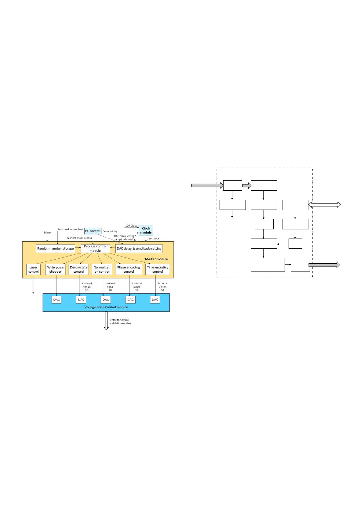
Design of V oltage Pulse Control Module for Free Space Measurement-Device-Independent Quantum Key Distribution Sijie Zhang, Nan Z hou, Fanshui Deng and Hao Liang Abstract —Measurement-Device-Independent Quantum Key Distribution (MDIQKD) protocol has been proved that it is unaffected by all hacking attac ks, and ensures the security of information theory even when the performance of single-photon detectors is not ideal. Fiber channel has been used by the previous MDIQKD experimental device. How ever, the signal attenuation increases exponentially as the transmission distance increases. In order to overcome t his, w e regar d free s pace as the channel of signal trans m i ssion, a nd the sig nal attenuation in c reases square as the trans mission d istance increases (regardless of the atmospheric scattering), w hich can effectively reduc e the signal attenuation trend. In order to implement the free space MDIQK D experiments, a modulation module is needed to modulate the wide pul se chopping, decoy-state, normalization, phase encoding a nd time encoding. In this p aper, we pre s ent the design of the Vo ltage Pulse Control Module for the free space MDIQKD. Index Ter m s —Voltage pulse control, ele ctronics d esign, free spac e MDIQKD. I. I NTRODU CTION OMP ARED with classical communication, the greatest advantage of q uantum co mmunication is sec urity. In the information society w h ere technology is in t he same intere st and pro sperity, peo ple are increasingl y de manding securit y, especially i n ar eas a nd sectors that require high security, such as military and financial services and so on. Quantum communication is alm o st the only choice for future secure communications. There are many research directions for Manuscript received June 1 , 2018. This work was supported in part b y the National Fundamental Research Prog ram und er Grants 2011CB921300, 2013CB336800, and 2011CBA00300, the National Natural Science Foundation of China, the Chinese Academy of Science, the Quantum Communication Technology Co., Ltd., A n hui, and the Shandong I nstitute of Quantum Science and Technol ogy Co., Ltd. S. J. Zhang, F. S. Deng, and H. Liang are with the State Key Laboratory of Particle Detection and Ele ct ronics, University of Science and Te ch nology of quantum communicatio n, and quantum cr yptography is the most important of which is the first pr actical field. Measurement-de vice-independent quant um key distrib ution (MDIQKD) p rotocol [1], [2], which is i mmune to all hacking attacks o n detectio n, guara ntees the securit y of information theoretically even with single-p hoton detectors, whose performance is not p erfect. Fiber channel is used b y the previous MDI QKD experimental d evice. Ho wever, the signal attenuation i ncreases e xponentiall y along with the tra nsmission distance increases. But using free space as the channel for signal transmission, with the signal attenuation increas es squarely (without consid ering the scatteri ng of the at mosphere), the signal attenuatio n trend can be effectively reduced. In order to implement free space MDIQKD experiments, a modulation module is needed to modulate the wide pulse chopping, decoy-state, normalization, phase e ncoding and time encoding. In this paper, we report our work on the design of voltage pulse contro l m od ule, focusi ng on the realization of pulse control using a wideband amplifier offering high d ynamic range, on the p revention o f waveform d istortion, a nd insufficient d rive capacity. The voltage pulse control module designed for the m od ulation of the optical module o f the free space MDIQKD has fulfilled the requirements o f the laborator y environment a nd is able to no w b e applied in an act ual experiments. And we did conduct jo int debugging of the enti re physical experi ment platform. China, Hefei, Anhui, 230026, China (e-mail: zsj2015@mail.ustc.e du.cn; dfsh@mail.ustc.e d u.cn; simonl h @ustc.edu.cn). N. Zhou, was with the State Key Laboratory of Particle De tection and Electronics, U niversity of Science and Technology of China, Hefe i 230026, China. He is now with Meiya Optoele ct ronics Technology Co., Ltd, He fei, Anhui, 230088, Chi n a (e-mail: zhoun@mail.ustc.edu.cn;). C II. D ESIGN A. System Structure The voltage pulse co ntrol module is used in the quantum cryptography s ystem, w i th t he m icro controller and DAC chip as the core. The modulation signal is generated under t he control o f the upper computer f o r m odu lating the light pulse that reaches the mod ulator. The main function of the voltage pulse control module [3] is as a modulation circuit, with a total of 5 Digital to Analog Converter (DAC) outputs. Respectively, t he wide p ulse chopper DAC has t wo adj ustable a mplitudes outpu ts(AC1, AC2), the deco y-state contr ol DAC has four adjustab le amplitudes outputs ( AD1, AD2, AD3, AD4) and the normalized co ntrol D AC has two adjustable amplit udes ( AU1, AU2). There are t wo adjustabl e a mplitudes o utputs ( AP1, AP 2) for the phase encoding co ntrol DAC a nd two adj ustable amplitudes outp uts (AT 1, AT2) for the t ime encod ing contr ol DAC. Figure. 1 illustrate the structure of the electronics system briefly. Specifications re quire that the output voltage o f all 5 DACs can be adjustable from 0V to 6V in 0.05V steps. And all 5 DACs have adjustable dela y times o f ± 15ns in 1 00ps ste ps. The rising edge o f the DAC output is about 1 ns, and the maximum output a mplitude can reach 7 V with a 50Ω impedance. Therefore, the power require ments of voltage pulse control module are re latively high. However, with the i ncrease of po wer, we can get a flatter p ulse, which can better serve t he subsequent optical modulation module. L ater , we w ill be going to im p lement the s ystem with a clock frequency of GHz. We expect the security key rate can b e further increa sed by increasing the clock frequency. B. Hardware In the volta ge pulse co ntrol module desig n, t he outpu t module of previous design f or the fiber channel MDI QKD uses THS3201 [4], which is a w i de gain band width, high spe ed current feedback amplifier of Texas Instrumen t s (TI), after tw o stages of amplificatio n, then o utputs t he voltage. B ut, there is still a need for a RF power a mplifier m od ule indep endent of the voltage pulse co ntrol module before it can be applied to the MDIQKD system. Ho wever, i n the new desi gn, we put the RF power a mplifier d irectly on the circuit boar d, so t hat w e can get enough p ower and stable voltage output only b y using the one stage operational ampli fier and the RF po wer amplifier. T his eliminates the need for an i ndependent RF po wer module and at the sa me time we get the o utput voltage what we need. The block d iagram o f the new d esign voltage p ulse contro l module is shown in the Figure 2. The signal flow of the entire m od ule is described as follows. As is seen in the Fig ure 2, the Low Voltage D ifferential Si gnal (LVDS) e nters the volta ge p ulse co ntrol module t hrough the connector and then is tra nsmitted to the LVDS transcei ver after signal selectio n. After level shifting, the signal level is converted to E mitter Coupled Logic (ECL), and then the signal flows into the s haping circuit and Voltage-controlled Gain Amplifier (VG A) amplificati on circuit. T he control s ystem sends a command to the voltage pulse co ntrol m o dule via the serial po rt to modulate the DA C outpu ts, which in t urn co ntrol the VGA outputs, th er eby modulating the output voltage pulse. III. T EST R ESULT S A. Laboratory en vironment test The tests ar e in pro gress an d we are also starti ng the p art work on the desi gn o f voltage pulse co ntrol module for th e GHz clock frequency. The test met hod we used currentl y is that t he input s ignal enters the voltage pulse control module from the master module of fiber channel system via t he connector. Then Fig. 1. The simplified structure of the e lectronic s system Micro controlle r Conn ector LV D S Transcei v er Sign al S w itchi ng Shapin g Circu i t VG A Amplifier DAC Operat ional Ampl i fier & RF Am plifier IMD C LV D S to EC L Mas te r mo dule signal Serial Tra ns ceiv e r Volta ge Pulse Co nt r ol Modul e Enter the optical modul ati on module Com mu nicate with PC Out put Fig. 2. Block diagr am of the voltage pulse control module the control system sends a co mmand to the voltage pulse control module throu gh the serial port, and the output s ignal is connected to the oscillos cope, which is the LeCro y WaveRunner 6 40Zi oscillosc ope [5] with a 4GHz bandwidth and a sampling ra te o f 40GS/ s, f o r o bserving th e out put voltage wavefor m. With a 50Ω loa d, the output wavefor m amplitude is up to 10Vpp. The output freque ncy meet s the e xperimenta l requirements, and the exper imental results show that the design index is satisfied. B. Physics experiment p latform test The results o f the current pr eliminar y tests are sho wn in Figure 3. Mo re detailed r esults of the j oint adjustment with the physics experi ment platform will be p rovided r ecently. The overall design a nd p roduction of the pro totype have been completed in April 2018 and are currently undergoing joint deployment w ith the ph ysical platfor m. T he entire electr onics system will be completed in J uly 2018 . After that, we will devote all our energy to the design of the voltage pulse contr ol module with a clock frequency of GHz based on this. By increasing the clock frequency, we b elieve that we can further increase the sec urity key rate. IV. C ONCLUSION This paper d escribes the design o f one electronic p art for quantum cryptograp hic system - volta ge pulse contro l module. For the voltage pulse generator, although it has i nitiall y reached the working re quireme nts and has been applied to the actual experiment t hrough the syste m jo int debugging, there ar e still so me areas for i mprovement. The increase in volta ge configuration spee d and elimination of signal edge j itter is the requirement for the next step. REFERENCES [1] H.-K. L o, M. Curty, and B. Qi, “Measure ment-Device-Independe n t Quantum Key Distribution,” Phys. Rev. L ett. , Vol. 108, Iss. 13 — 30 March 2012. [2] Y. L . Tang, H. L. Yin, S. J. Che n, Y. Liu, W. J. Zhang, X. Jiang, L. Zhang, J. Wang, L. X. Yo u, J. Y. Guan, D. X. Yang, Z. Wang, H. Liang, Z. Zhang, N. Zhou, X. F. Ma, T. Y. C h en, Q. Zhang , and J. W. Pan, “Meas urement-Device- Independent Quantum Key Distribution ove r 200 km,” Phys. Rev. Lett., Vol. 113, Iss. 19 — 7 Nov ember 2014. [3] Q. L iu, “De sign of voltage pulse generator and voice data transmission module for quantum sec u rity communication sy stem” M.S. thesis, Dept. Modern. Phys., UST C., Hefei, A n hui, Chi n a, 2008. [4] THS3201: 1.8-GHz, Low Distortion, Current Feedback Amplifiers Data Manual, Texas I nstru ments, Dall as, Texas, USA, 2009. [5] WaveRunner 6 Zi Oscilloscopes (400 MHz - 4 GHz) Data Manual, LeCroy , Ch estnut Ridge, New York, USA, 2017. Fig. 3. Preliminary test results 0 1 2 3 4 5 6 7 0 2 4 6 8 10 OUTPUT/V Control System /V Preliminary Test Results Phase Decoy Time I Time II Normal ization
Original Paper
Loading high-quality paper...
Comments & Academic Discussion
Loading comments...
Leave a Comment