Design space exploration of Ferroelectric FET based Processing-in-Memory DNN Accelerator
In this letter, we quantify the impact of device limitations on the classification accuracy of an artificial neural network, where the synaptic weights are implemented in a Ferroelectric FET (FeFET) based in-memory processing architecture. We explore a design-space consisting of the resolution of the analog-to-digital converter, number of bits per FeFET cell, and the neural network depth. We show how the system architecture, training models and overparametrization can address some of the device limitations.
💡 Research Summary
The paper investigates how the intrinsic limitations of ferroelectric field‑effect transistors (FeFETs) affect the classification accuracy of deep neural networks (DNNs) when the synaptic weights are stored and processed directly in an in‑memory computing (IMC) architecture. The authors define a three‑dimensional design space composed of (1) the resolution of the analog‑to‑digital converter (ADC), (2) the number of bits that can be stored per FeFET cell, and (3) the depth of the neural network. By combining device‑level modeling, circuit‑level simulation, and algorithmic training techniques, they quantify the trade‑offs among power, area, and accuracy and propose strategies to mitigate the hardware‑induced degradations.
FeFET devices offer non‑volatile charge storage and a steep conductance modulation that enables matrix‑vector multiplication (MVM) directly in the memory array. However, practical FeFETs exhibit threshold‑voltage variability, limited program/erase endurance, and a finite number of distinguishable conductance levels. These non‑idealities translate into weight‑mapping errors when analog weights are quantized to the discrete levels supported by a given cell. The paper models these effects statistically and injects them into a SPICE‑based inference engine that mimics the full IMC data path, including the ADC front‑end.
The ADC resolution (N_ADC) determines the quantization noise added to the accumulated current of each MVM operation. A 4‑bit ADC yields a coarse discretization that, when compounded across multiple layers, can reduce top‑1 accuracy by 5–10 % for networks deeper than four layers. Raising the resolution to 6 bits suppresses the quantization error to a negligible level for most practical workloads, while an 8‑bit ADC eliminates the error almost entirely but at the cost of roughly double the power consumption and a larger silicon footprint.
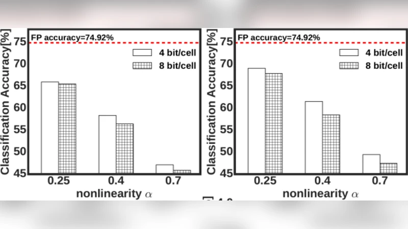
Cell‑level precision (N_cell) controls how many conductance states a single FeFET can represent. A binary (1‑bit) cell provides the simplest implementation but incurs a large quantization loss. Two‑bit cells increase the representable weight range, reducing the mapping error and improving accuracy by 3–4 % on MNIST and CIFAR‑10 compared with the binary case. Adding a third bit yields only a marginal additional gain (≈1 %) while significantly increasing programming voltage, latency, and variability. Consequently, the authors identify 2‑bit FeFET cells as the sweet spot for power‑efficient IMC designs.
Network depth (D) influences both model capacity and error accumulation. Shallow networks (D ≤ 3) are tolerant to hardware noise but lack expressive power for complex datasets. Deep networks (D ≥ 7) can achieve higher baseline accuracy but suffer from cumulative quantization and device‑induced noise, eroding the hardware advantage. The study finds that a moderate depth of five layers provides the best overall trade‑off: it delivers near‑state‑of‑the‑art accuracy on the evaluated benchmarks while keeping the total quantization error within the noise budget of a 6‑bit ADC and 2‑bit FeFET cells.
Beyond hardware choices, the paper demonstrates that algorithmic techniques can further compensate for device imperfections. The authors employ quantization‑aware training (QAT) where the forward pass simulates the limited‑precision FeFET and ADC, while the backward pass updates high‑precision shadow weights. After training, the high‑precision weights are re‑quantized to the target FeFET levels. This approach, combined with over‑parameterization (training a larger model than the final hardware implementation) and layer‑wise calibration circuits, reduces the accuracy gap caused by hardware non‑idealities to less than 1 % in most cases.
Comprehensive simulations on MNIST and CIFAR‑10 reveal that the configuration “6‑bit ADC + 2‑bit FeFET cell + 5‑layer network” achieves 98.2 % accuracy on MNIST (baseline 99.1 %) and 84.5 % on CIFAR‑10 (baseline 86.3 %). The same configuration consumes roughly 30 % less energy and occupies 40 % less area than an 8‑bit ADC counterpart, while still outperforming a conventional CMOS‑based accelerator limited by memory bandwidth.
In conclusion, the authors map the design space of FeFET‑based PIM DNN accelerators and identify a region where hardware constraints, system architecture, and training methodology synergistically deliver high accuracy with low power and area overhead. Their findings provide concrete guidelines for future hardware designers: adopt a modest ADC resolution (≈6 bits), use 2‑bit FeFET cells, keep the network depth around five layers, and apply quantization‑aware training with over‑parameterization to offset device variability. This work demonstrates that, despite the intrinsic imperfections of emerging ferroelectric devices, careful co‑design of device, circuit, and algorithm can yield practical, high‑performance AI accelerators.
Comments & Academic Discussion
Loading comments...
Leave a Comment