Towards Ultra-low-power Realization of Analog Joint Source-Channel Coding using MOSFETs
Certain sensing applications such as Internet of Things (IoTs), where the sensing phenomenon may change rapidly in both time and space, requires sensors that consume ultra-low power (so that they do not need to be put to sleep leading to loss of temporal and spatial resolution) and have low costs (for high density deployment). A novel encoding based on Metal Oxide Semiconductor Field Effect Transistors (MOSFETs) is proposed to realize Analog Joint Source Channel Coding (AJSCC), a low-complexity technique to compress two (or more) signals into one with controlled distortion. In AJSCC, the y-axis is quantized while the x-axis is continuously captured. A power-efficient design to support multiple quantization levels is presented so that the digital receiver can decide the optimum quantization and the analog transmitter circuit is able to realize that. The approach is verified via Spice and MATLAB simulations.
💡 Research Summary
**
The paper addresses the pressing need for ultra‑low‑power, low‑cost sensing nodes in emerging Internet‑of‑Things (IoT) and dense wireless sensor network (WSN) deployments. Conventional joint source‑channel coding (JSCC) implementations rely on digital microcontrollers and analog‑to‑digital converters (ADCs), which consume hundreds of microwatts—far beyond the power budget of energy‑harvesting sensors that typically generate only tens of microwatts. To overcome this limitation, the authors propose an entirely analog JSCC (AJSCC) architecture that uses the current‑voltage (I‑V) characteristics of a single MOSFET operating in its saturation region as the space‑filling curve for encoding two sensor variables (x and y) into a single analog signal.
In the proposed scheme, the gate‑to‑source voltage (Vgs) represents the quantized y‑axis and is limited to a discrete set of levels determined by a configurable quantization step φ. The drain‑to‑source voltage (Vds) captures the continuous x‑axis. By applying Vgs and Vds to a MOSFET, the resulting drain current (Ids) uniquely encodes the pair (Vgs, Vds) according to the MOSFET’s saturation equation: Ids = ½·(W/L)·μ·Cox·(Vgs‑Vth)²·(1+λ·Vds). The channel‑length‑modulation parameter λ causes Ids to increase slowly with Vds, providing a measurable slope that can be exploited at the receiver.
A key contribution is the decoding method. Because a single Ids value can be generated by multiple (Vgs, Vds) pairs, the authors use a “slope‑matching” technique: two consecutive Ids samples are taken, their slope (ΔIds/ΔVds) is computed, and the Vgs level whose theoretical slope (≈ λ·Ids) best matches the measured slope is selected. This approach assumes that the sensed physical phenomenon and the wireless channel vary slowly relative to the sampling rate, so consecutive samples lie on the same Vgs curve with high probability.
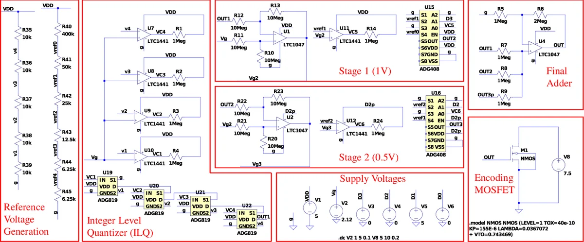
To support adaptive resolution, the authors design a front‑end “precircuit” that quantizes the raw Vgs input according to the chosen φ. The precircuit consists of an integer‑level quantizer (ILQ) followed by up to four residual‑correction stages. Each stage handles one binary digit of the quantization step; a one‑hot control vector (φ3, φ2, φ1, φ0) selects the active stage and powers down unused stages, thereby saving energy. The quantized Vgs (Vgs,MOS) is then fed to the MOSFET, and the resulting Ids is frequency‑modulated for RF transmission. No digital processing is required at the sensor node.
Power consumption is a central metric. Using a 0.18 µm n‑MOSFET model (W·µ·Cox/L = 155 µF/V·s, Vth ≈ 0.74 V, λ = 0.037 V⁻¹), SPICE simulations show that the entire encoder (precircuit plus MOSFET) draws roughly 24 µW, with potential reductions to ≈ 8 µW through layout and bias optimizations. This represents a 3‑ to 10‑fold improvement over prior analog AJSCC implementations (Design 1: 130 µW, Design 2: 72 µW). MATLAB simulations validate the decoding accuracy: for φ = 0.5 V the root‑mean‑square error (RMSE) of both Vgs and Vds after correction is low; smaller φ values (0.25 V, 0.125 V) exhibit higher RMSE due to op‑amp saturation in the precircuit, a limitation the authors acknowledge and suggest can be mitigated with better analog design.
The paper also explores the impact of λ variations on decoding performance. Larger λ values increase the slope of the Ids‑Vds curves, improving the discriminability of different Vgs levels and reducing RMSE. This insight suggests that device‑level engineering (e.g., choosing MOSFET geometries or biasing conditions that enhance λ) can further boost system robustness against process and temperature variations.
Overall, the work makes several notable contributions:
- Introduces a novel MOSFET‑based space‑filling curve for AJSCC, eliminating the need for power‑hungry digital components.
- Provides a configurable quantization front‑end that can adapt resolution to application‑specific dynamic ranges.
- Demonstrates ultra‑low power operation (≈ 24 µW, potentially ≤ 8 µW) suitable for energy‑harvesting sensor nodes.
- Validates the concept through comprehensive SPICE and MATLAB simulations, including analysis of quantization errors and device‑parameter sensitivities.
Future research directions identified include silicon‑level prototype fabrication, experimental validation over realistic wireless channels, extension to multi‑dimensional source vectors (beyond two variables), and integration with ultra‑low‑power RF front‑ends. By showing that MOSFET physics can be directly harnessed for joint source‑channel coding, the paper opens a new pathway for designing truly battery‑free, high‑density IoT sensing infrastructures.
Comments & Academic Discussion
Loading comments...
Leave a Comment