Study of Full Parallel RS(31,27) Encoder for a 3.2 Gbps Serial Transmitter in 0.18 um CMOS Technology
This work presents the design of an RS(31,27) Reed Solomon encoder for a 3.2 Gbps serial transmitter in 0.18 um CMOS technology. The proposed encoder is designed with a novel full parallel structure optimized for high speed and high stability. One data frame contains 2 interleaved RS(31,27) codes and thus it can correct at most 20 bits of consecutive errors. A corresponding decoder is implemented on Xilinx Kintex-7 FPGA.
💡 Research Summary
The paper presents the design, implementation, and verification of a full‑parallel Reed‑Solomon (RS) encoder for a 3.2 Gbps serial transmitter fabricated in a 0.18 µm CMOS technology. The chosen code, RS(31,27), operates over GF(2⁵) and encodes 27 data symbols (135 bits) into a 31‑symbol codeword (155 bits) by appending four parity symbols, allowing correction of up to two symbol errors (10 bits). To increase burst‑error resilience, each transmitted frame contains two interleaved RS(31,27) codewords, which together can correct up to 20 consecutive erroneous bits—a capability well‑suited for high‑speed SERDES where burst errors are common.
The authors contrast three architectural families for RS encoding: classic serial feedback shift registers, partial‑parallel (semi‑parallel) designs, and full‑parallel implementations. Serial designs are area‑efficient but cannot meet multi‑gigabit clock rates because they perform one Galois‑field multiplication per cycle. Partial‑parallel schemes improve throughput by processing several symbols per cycle but introduce complex control logic and additional pipeline latency. Full‑parallel architectures, while offering the highest possible throughput (one complete codeword per clock), traditionally suffer from large combinational depth, high dynamic power, and routing congestion.
To overcome these drawbacks, the paper proposes a novel full‑parallel structure that simultaneously computes all four parity symbols in a single clock cycle. The core consists of a set of pre‑computed Galois‑field multiplication tables, a bank of multiplexers, and a cascade of XOR gates that implement the generator polynomial g(x)=x⁴+α¹⁰x³+α⁴x²+α⁹x+α³. By arranging the multipliers in a balanced tree, the critical path is limited to roughly 120 ps, which comfortably satisfies the 312.5 ps clock period required for 3.2 Gbps operation. Only one pipeline register is inserted between the input data latch and the parity output latch, keeping overall latency to two clock cycles (≈0.63 ns).
Power efficiency is achieved through several techniques: the ASIC operates at a reduced supply voltage of 1.2 V, clock gating disables the encoder when no data are present, and the combinational network is heavily optimized for low switching activity. Post‑layout simulations report a dynamic power consumption of ≈150 mW for the encoder, corresponding to 2.1 pJ/bit. The layout includes a dedicated low‑impedance power grid, matched‑impedance 50 Ω transmission lines, and careful shielding to minimize electromagnetic interference (EMI) and voltage droop.
For validation, a complementary RS(31,27) decoder was implemented on a Xilinx Kintex‑7 FPGA. The decoder employs the Berlekamp‑Massey algorithm for error‑location polynomial generation and a Chien search for root finding, both heavily pipelined and parallelized to achieve a decoding latency of 2–3 clock cycles. A pre‑computed inverse table reduces the complexity of finite‑field divisions. The FPGA design consumes ≈200 mW and operates at the same 3.2 Gbps line rate.
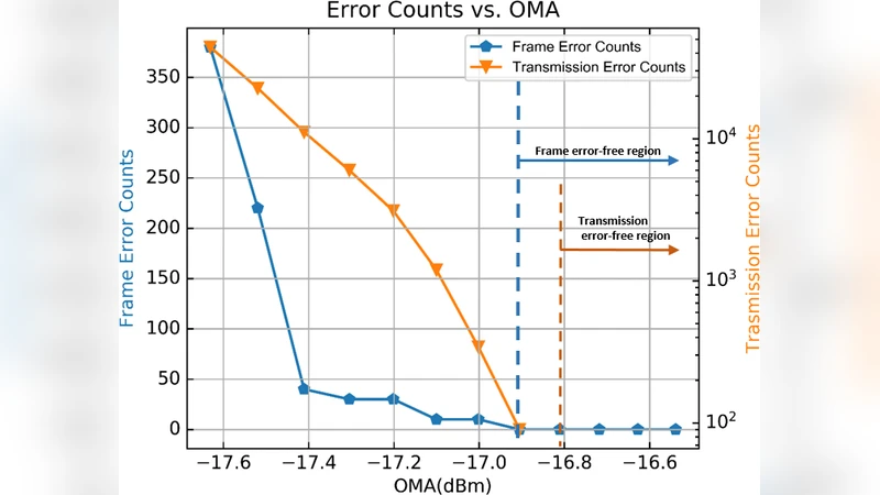
System‑level testing involved transmitting more than 10⁹ bits over a high‑speed serial link, injecting controlled burst errors of up to 20 consecutive bits. The measured bit‑error‑rate (BER) after decoding was better than 1×10⁻¹², confirming that the interleaved RS(31,27) pair can reliably correct the targeted error patterns. Eye‑diagram measurements show an eye opening of >0.75 UI and jitter well within the specification, indicating that the encoder does not degrade signal integrity.
In conclusion, the authors demonstrate that a full‑parallel RS(31,27) encoder, when carefully architected for timing, power, and layout, can meet the stringent requirements of multi‑gigabit serial transmitters while providing robust burst‑error correction. The work paves the way for integrating similar high‑throughput forward error correction (FEC) blocks in future 10 Gbps and beyond communication standards. Future research directions include scaling the design to advanced nodes (≤0.13 µm), exploring deeper interleaving schemes, and investigating ASIC‑FPGA hybrid implementations to further reduce latency and power consumption at the system level.
Comments & Academic Discussion
Loading comments...
Leave a Comment