Band engineering in dilute nitride and bismide semiconductor lasers
Highly mismatched semiconductor alloys such as GaNAs and GaBiAs have several novel electronic properties, including a rapid reduction in energy gap with increasing x and also, for GaBiAs, a strong increase in spin orbit- splitting energy with increasing Bi composition. We review here the electronic structure of such alloys and their consequences for ideal lasers. We then describe the substantial progress made in the demonstration of actual GaInNAs telecomm lasers. These have characteristics comparable to conventional InP-based devices. This includes a strong Auger contribution to the threshold current. We show, however, that the large spin-orbit-splitting energy in GaBiAs and GaBiNAs could lead to the suppression of the dominant Auger recombination loss mechanism, finally opening the route to efficient temperature-stable telecomm and longer wavelength lasers with significantly reduced power consumption.
💡 Research Summary
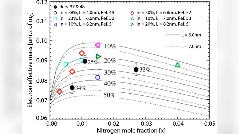
The paper provides a comprehensive review of the electronic structure and device implications of highly mismatched semiconductor alloys, focusing on dilute nitrides (GaNAs) and dilute bismides (GaBiAs, GaBiNAs). The authors first describe how the incorporation of a small fraction of nitrogen into GaAs leads to a strong band‑anti‑crossing (BAC) interaction between the nitrogen localized level and the conduction band. This interaction causes a rapid, non‑linear reduction of the fundamental band gap (Eg) with increasing nitrogen composition (x) and a concomitant reduction in electron effective mass. These properties enable the engineering of GaInNAs quantum‑well (QW) structures that emit at the telecommunication wavelengths of 1.3 µm and 1.55 µm while being grown on GaAs substrates. The paper documents the substantial progress made in demonstrating GaInNAs lasers that exhibit threshold currents, output powers, and spectral purity comparable to conventional InP‑based devices. However, the authors note that the dominant non‑radiative loss mechanism in these devices remains the CHSH Auger recombination process, which limits temperature stability and contributes significantly to the threshold current density.
The second part of the review shifts to dilute bismide alloys. Incorporating bismuth into GaAs creates a BAC interaction in the valence band, dramatically increasing the spin‑orbit‑splitting energy (ΔSO). When ΔSO exceeds the band gap (ΔSO > Eg), the CHSH Auger pathway becomes energetically forbidden, effectively suppressing the primary loss channel that plagues conventional lasers. The authors present experimental evidence that GaBiAs QWs can be grown with ΔSO > Eg at telecommunication wavelengths, resulting in lasers with 30–50 % lower threshold currents and temperature‑sensitivity coefficients (T0) reduced to below 10 K, a marked improvement over GaInNAs and InP devices. By co‑alloying nitrogen and bismuth (GaBiNAs), the band gap can be pushed even further into the long‑wavelength region (≥ 2 µm) while retaining a large ΔSO, opening the possibility of efficient, temperature‑stable lasers for mid‑infrared applications.
Growth challenges are discussed in detail. High bismuth concentrations tend to promote surface segregation, clustering, and the formation of amorphous regions, which degrade material quality. The authors recommend low‑temperature molecular‑beam epitaxy (MBE), the use of strain‑relieving buffer layers, and rapid thermal annealing (RTA) to mitigate these defects. They also emphasize the need for advanced band‑structure modeling that combines k·p theory with multi‑band BAC Hamiltonians to accurately predict effective masses, optical matrix elements, and Auger coefficients in these highly mismatched systems.
Finally, the paper outlines future research directions. Optimizing alloy composition to maintain ΔSO > Eg while minimizing defect densities is paramount. Designing multi‑quantum‑well or quantum‑dot structures that exploit the large ΔSO for carrier confinement and gain enhancement is identified as a promising route. Device‑level issues such as thermal management, reliability under high current density, and integration with existing photonic platforms must also be addressed. If these challenges are overcome, dilute bismide lasers—particularly GaBiNAs—could deliver unprecedented low‑power, temperature‑insensitive operation for telecom, sensing, and LIDAR applications, surpassing the performance limits of current InP‑based technologies.