Integrated Conductivity-Modulation-Based RF Magnetic-Free Non-Reciprocal Components: Recent Results and Benchmarking
Achieving non-reciprocity and building nonreciprocal components through spatio-temporal modulation of material properties has attracted a lot of attention in the recent past as an alternative to the more traditional approach of exploiting Faraday rot…
Authors: Negar Reiskarimian, Aravind Nagulu, Tolga Dinc
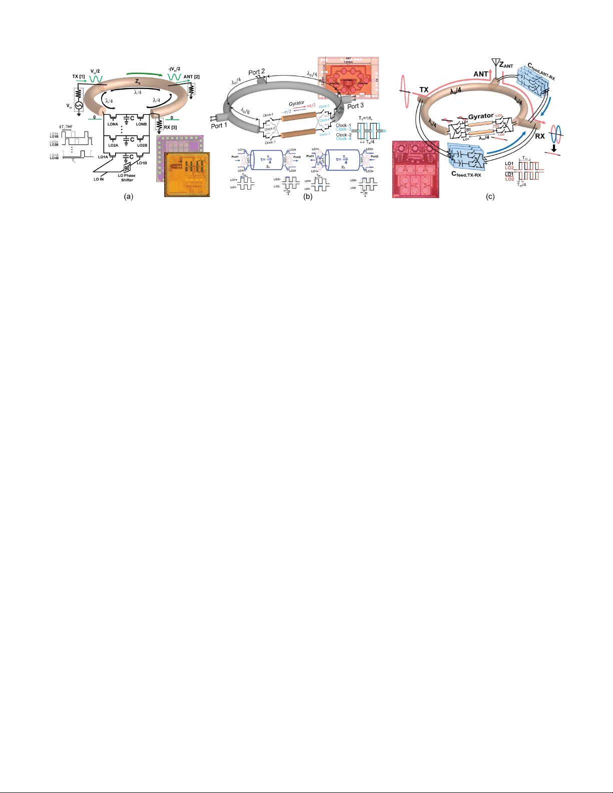
SUBMITTED TO IEEE ANTENN AS AND WIRELESS PR OP A GA TION LETTERS 1 Inte grated Conducti vity-Modulation-Based RF Magnetic-Free Non-Reciprocal Components: Recent Results and Benchmarking Negar Reiskarimian, Student Member , IEEE, Aravind Nagulu, Student Member , IEEE, T olga Dinc, Member , IEEE, and Harish Krishnaswamy , Member , IEEE, Abstract —Achieving non-recipr ocity and building non- recipr ocal components through spatio-temporal modulation of material pr operties has attracted a lot of attention in the r ecent past as an alternative to the more traditional approach of exploit- ing Faraday r otation in magnetic materials. In this letter , we re- view recent resear ch on spatio-temporal conducti vity-modulation, which enables low-loss, small-f ootprint, wide-bandwidth and high-power -handling non-r eciprocal components operating from radio frequencies (RF) to millimeter-wa ves (mm-waves) and inte- grated in a CMOS platf orm. Four generations of non-r eciprocal circulators and circulator -based systems will be reviewed. W e will also discuss metrics of perf ormance that are important for wireless applications and standards, and intr oduce a new antenna (ANT) interface efficiency figure of merit ( η AN T ) to enable a fair comparison between v arious types of antenna interfaces. I . I N T R O D U C T I O N R ECIPR OCITY mandates the same signal transmission profile for wa ves propagating in opposite directions between two points in space. V arious theorems of reciprocity has been formulated over the years, including the work of Green (electrostatics), Rayleigh (dynamic systems), Helmholtz (optics, acoustics) and Lorentz (electromagnetics) [1]. Lorentz reciprocity is a fundamental physical precept that characterizes the vast majority of electronic and photonic materials, circuits and components. Non-reciprocal components, such as circulators, isolators, gyrators and non-reciprocal phase-shifters, are critical for vari- ous RF and mm-w ave applications, including communications, radar , imaging and sensing. Specifically , high-performance circulators can find application as the shared-antenna inter- face of transceivers for emerging wireless communication paradigms such as full-duplex (FD) [2]–[4] and FD multiple- input multiple-output (MIMO) systems [5], and in frequency- modulated continuous-wa ve (FMCW) radar . FD aims to in- stantly double the link capacity in the physical layer by simul- taneously transmitting and receiving at the same frequency , as well as providing other benefits in the higher layers [3], [4]. Reciprocity can be violated by breaking one of three neces- sary conditions - time-inv ariance, linearity or by exploiting materials with an asymmetric permitti vity or permeability tensor . T raditionally , non-reciprocity has been achie ved by using magnetic materials such as ferrites, which lose their reci- procity under the application of an external biasing magnetic field. Such magnetic non-reciprocal components are limited in their applicability , since ferrites are incompatible with IC fabrication processes and a permanent magnet is required to induce the magneto-optic Faraday ef fect [6]. This causes the resulting non-reciprocal element to be b ulky , expensi ve and incompatible with CMOS integration. The oldest alternativ e to using magnets is to exploit the inherent non-reciprocity of activ e current/voltage-biased transistors [7]–[9]. Such an approach is compatible with IC fabrication, b ut is limited by the noise and nonlinearity introduced by the active devices [10]. Breaking reciprocity through nonlinearity has also been explored at RF [11] as well as in the optical domain [12]. Howe v er , the signal-po wer-dependent performance limits the applicability of this approach. In recent years, there has been progress on breaking reciprocity through time-variance, specifically spatio-temporal modulation of material parameters. Such approaches are the- oretically linear to the desired signal and noise free. Early approaches hav e focused on permittivity as the modulated parameter [13]–[21]. In the optical domain, permitti vity is modulated through electro-optic or acousto-optic interactions, but the modulation inde x is typically extremely weak. In the RF domain, permittivity modulation is achiev ed using v arac- tors which too e xhibit limited modulation index ( C max /C min is usually around 2 − 4 ). A weak modulation index directly translates to a lar ge de vice size ov er which modulation must be performed. V aractors, and permittivity modulation in general, also exhibit a trade-of f between modulation index and loss, particularly as the operating frequency is increased. Conse- quently , these efforts hav e resulted in designs that exhibit a trade-off between loss, size, bandwidth and linearity . In the circuits community , time-modulated systems are com- monly called linear periodically-time-varying (LPTV) circuits. Early reports on LPTV circuits date back to the 1940s [22]. In the following two decades, a class of LPTV circuits and systems also referred to as commutated networks attracted a lot of attention, and theoretical [23], [24] and practical aspects [25] of their implementation were explored. More recently , commutated networks have emerged once again as a hot topic of research, primarily due to the ability to realize tunable RF high-quality-factor filters (the so-called N-path filters) in CMOS for the first time [26]–[28]. Recently , we found that commutated networks have a rich set of unique properties that go beyond high-Q filtering, including the ability to realize non- reciprocity [29]–[34]. In this letter, we will cov er our recent research on using commutated circuits to break reciprocity and build high- SUBMITTED TO IEEE ANTENNAS AND WIRELESS PROP AGA TION LETTERS 2 Fig. 1: Conceptual diagrams of our conductivity-modulation-based circulators: (a) RF N-path-filter -based circulator and circulator-recei ver architecture employing a linearity-enhancement technique for transmitter side excitations [30], [31]. (b) Millimeter-w av e switched-transmission-line circulator [32], [33]. (c) RF switched-transmission-line circulator with > 1W power - handling capability and inductor-free antenna balancing [34]. performance passiv e circulators operating from RF to mm- wa ve frequencies in CMOS. Our switch-based commutated cir cuits may be fundamentally understood as performing spatio-temporal conductance modulation, and lever age the fact that conductivity is a variable material pr operty that is unique to semiconductors. Conductivity in semiconductors can be modulated o ver a wide r ange (CMOS switch ON/OFF conductance ratios can be as high as 10 3 − 10 5 ) r elative to permittivity . In Section II, we will describe the fundamental physical principles, as well as four generations of CMOS cir- culators and circulator-based wireless communication systems [30]–[34] targeting emerging full-duplex and 5G mm-wa ve applications. W e will also cover architectural concepts that improv e the linearity and isolation. In Section III, we discuss various metrics of performance that are critical for wireless applications, and introduce a ne w antenna interface ef ficiency figure of merit ( η AN T ) that enables a fair comparison be- tween v arious reciprocal and non-reciprocal shared-antenna interfaces. Finally , Section IV concludes the paper . I I . C O N D U C T I V I T Y - M O D U L A T I O N - B A S E D N O N - R E C I P R O C I T Y A. N-P ath-Filter -Based Circulator and Cir culator-Receiver Ar chitectur e N-path filters enable the implementation of reconfigurable, high- Q filters at RF in nanoscale CMOS IC technology [26], and are a class of LPTV networks where the signal is periodically commutated through a bank of capacitors. W e hav e found that applying a relativ e phase shift to the non- ov erlapping clocks dri ving the input and output switch sets of a two-port N-path filter imparts a non-reciprocal phase-shift to the signals trav eling in the forward and re verse directions since they see a dif ferent ordering of the phase-shifted switches [35]. Essentially , the two-port N-path filter with a clock phase shift of 90 ◦ r ealizes an electrically-infinitesimal gyrator . T o con v ert phase non-reciprocity to non-reciprocal wa ve propagation, an N-path-filter with ± 90 ◦ phase-shift is placed inside a transmission line loop with a length of 3 λ /4 (Fig. 1(a)). The combination of the non-reciprocal phase shift of the N-path filter with the reciprocal phase shift of the transmission line results in unidirectional wave propagation ( − 270 ◦ − 90 ◦ = − 360 ◦ ), because the boundary condition for wa ve propagation in the rev erse direction can not be satisfied ( − 270 ◦ +90 ◦ = − 180 ◦ ). Additionally , a three-port circulator can be realized by placing ports an ywhere along the loop as long as they maintain a λ /4 circumferential distance between them. Inter estingly , maximum linearity with r espect to the transmitter (TX) port is achie ved if the r eceiver (RX) port is placed adjacent to the N-path filter , since the inher ent TX-RX isolation suppr esses the voltage swing on either side of the N-path filter , enhancing its linearity . T able I lists the performance metrics of a 750MHz 65nm CMOS N-path-filter-based circulator , whic h is the first CMOS passive cir culator to be implemented [29], [30]. Furthermore, the N-path filter in the circulator can be repurposed as a down-con v erting mixer , directly providing the baseband recei ved signals on the N-path filter capacitors. More details about this work can be find in [31]. B. W ideband Millimeter-W ave Swithced-T ransmission-Line- Based Non-Recipr ocal Cir culator Inspired by the N-path-filter -based RF circulator discussed in the previous subsection, we proposed a generalized conduc- tivity modulation concept using switched transmission lines [32], [33]. The concept, shown in Fig. 1(b), consists of two sets of differential mixer -quad switches on either end of a differential transmission-line delay (replacing the commutated capacitors). The switches are clocked at a modulation fre- quency ω m , and the delay of the line is equal to one quarter of the modulation period ( T m / 4 ). The switches are clocked with 50% duty-cycle square-wa ve clocks with a relativ e phase shift of T m / 4 . As a result of this, wav es traveling from left to right experience the transmission-line delay with no sign flips in both halves of the clock period. On the other hand, wav es trav eling from right to left experience the transmission-line delay along with one sign flip. In other words, transmission in both directions is perfectly lossless, but there is an infinitely broadband 180 ◦ non-reciprocal phase dif ference. In other wor ds, the structur e r ealizes an infinitely broadband gyrator . SUBMITTED TO IEEE ANTENNAS AND WIRELESS PROP AGA TION LETTERS 3 Fig. 2: FD wireless communication link using shared-antenna interface. Similar ideas related to switched transmission lines to realize broadband non-reciprocity hav e been explored in [36], [37]. The ke y aspect of this architecture is that the infinite bandwidth of the gyrator implies that the signal frequency and the modulation frequency are completely decoupled. An arbitrarily low modulation frequency can be used, with the only restriction being an associated increase in the transmis- sion line length, and hence, loss. This benefit was exploited to realize a mm-wave (25GHz) fully-integrated passiv e circulator in 45nm SOI CMOS, shown in Fig. 1(b) [32], [33], by once again placing a 3 λ/ 4 transmission line around the gyrator . Modulation was performed at 1/3rd of the operating frequency (8.33GHz). The lowering of the modulation frequenc y , as well as the need for 50% duty-cycle clocks, as opposed to numerous low-duty-cycle clocks as in N-path filters, is critical as clocking switches at mm-wav e frequencies is impractical in current CMOS IC technology . The infinitely-broadband phase non-reciprocity also implies broader bandwidth of operation for the resultant circulator . A summary of the performance of the 25GHz prototype can be found in T able I. C. Highly Linear RF Non-Recipr ocal Cir culator with Loss- F r ee , Inductor-F ree Antenna Balancing Fig. 1(c) sho ws the architecture of a highly-linear RF circulator , which uses the feature of lowering the modulation frequency to enhance the po wer handling and linearity of the circulator at 1GHz operating frequency . The switches were modulated at 333MHz for 1GHz operation, and such a lo w modulation frequency enables the usage of the thick-oxide devices in 180nm SOI CMOS technology to boost power handling. The measured in-band TX-ANT/ANT -RX input third-order intercept points (IIP3) are +50dBm and +36.9dBm respectiv ely . TX-ANT input 1dB compression point (P1dB) is > +30.7dBm (limited by the measurement setup), at which point the compression is only 0.66dB, while the ANT -RX input P1dB is +21dBm. This implementation notably improv es linearity and po wer handling by 10-100 × when compared with our prior CMOS non-reciprocal circulators [34]. The TX-RX isolation of all shared-antenna interfaces is limited by the matching of the antenna port, which necessitates an antenna tuning mechanism. T raditionally , magnetic circu- lators are followed by antenna tuners. In this work, antenna balancing is achie ved by implementing digitally pr ogrammable feed capacitor banks between TX-RX and ANT -RX ports. Due to the − 90 ◦ phase dif ference between the TX and ANT ports and the programmable nature of the feed capacitors, this produces tunable orthogonal currents which can cancel the leakage at the RX port produced by an antenna mismatch (Fig. 1(c)). The fully-dif ferential architecture enables a free sign flip in the feed capacitor banks, and therefore allows complete VSWR cov erage without using any inductiv e or resistiv e elements in the feed circuitry . Aggressi ve de vice stacking is employed in the static switches used in these feed capacitor banks so that they do not limit linearity and po wer handling. The ability to compensate a VSWR of up to 1.85 (and beyond) was demonstrated in this work. A summary of the performance of the prototype can be found in T able I. I I I . A N T E N NA I N T E R FA C E E FFI C I E N C Y F O M An ideal antenna interface should hav e no loss, extremely high po wer handling and no additional po wer consumption. Con ventional three-port reciprocal antenna interfaces, such as hybrids or electrical-balance duple xers (EBDs) [38]–[41], hav e high power handling but exhibit a fundamental 3dB loss, with an additional ≈ 1dB loss due to implementation issues such as finite metal resisti vity and substrate loss. LPTV circulators hav e lower loss than reciprocal interfaces, but only recently hav e been achie ving comparable po wer handling and require additional po wer consumption. Hence, to enable a fair compar - ison between various shared-antenna interfaces, an FoM called antenna interface efficiency ( η AN T ) is introduced. It calculates the degradation imparted to the transmitter efficienc y by the antenna interface by assuming a certain baseline efficienc y . 1) Metrics for P ower Handling: Before introducing the new FoM, it is important to discuss the different metrics that deter- mine the TX-port power handling of an ANT interface. The most common metrics are TX-port input P1dB and IIP3. T ypi- cally , communication systems operate with P1dB as the upper limit of the transmitted signal power . IIP3 captures the in-band intermodulation distortion produced on the input signal by the nonlinearity of the interface. This distortion is mainly relev ant as it leaks into adjacent channels (a phenomenon commonly called spectral re gr owth ), potentially desensitizing other users. T ypical wireless standards mandate a certain adjacent-channel leakage ratio (A CLR). Loosely , operating 20dB below the IIP3 lev el keeps the leakage into adjacent channels 40dB below the main signal power . SUBMITTED TO IEEE ANTENNAS AND WIRELESS PROP AGA TION LETTERS 4 T ABLE I: Comparison T able [30] [32] [38] [34] Architecture N-path-filter circulator Switched-t-line mm-wave circulator Electrical-balance duplexer Highly-linear RF circulator T echnology 65nm CMOS 45nm SOI CMOS 180nm SOI CMOS 180nm SOI CMOS Frequency 0.61 - 0.975GHz 25GHz 1.9 - 2.2GHz 0.86 - 1.08GHz TX-ANT/ANT -RX Trans. -1.7/-1.7dB -3.3/-3.2dB -3.7/-3.9dB -2.1/-2.9dB Isolation BW 1.9 % ( > 25dB), 0.33 % ( > 40dB) 18 % ( > 18.5dB) 2 15 % ( > 40dB) 17 % ( > 25dB), 3.1 % ( > 40dB) Z AN T impedance 50 Ω 50 Ω 1.5:1 VSWR 1.85:1 VSWR ANT -RX NF 4.3dB 3 3.3 - 4.4dB 3.9dB 3.1dB TX-ANT IIP3/P1dB +27.5dBm/ N/R +20.1dBm/ > +21.5dBm +70dBm/ > +27dBm +50.025dBm/ > +30.66dBm ANT -RX IIP3/P1dB +8.7dBm/ N/R +19.9dBm/ > +21dBm +72dBm/ > +27dBm +36.9dBm/+21.01dBm TX-induced RX P1dB N/R N/R N/R +21.3dBm Power Consumption 59 mW 78.4mW 0mW 170mW Chip Area λ 2 / 6400 or 25mm 2 4 λ 2 / 66 or 2.16mm 2 λ 2 / 13000 or 1.74mm 2 λ 2 / 5500 or 16.5mm 2 η AN T 5 7.2 % > 14.9 % 13.8 % > 23.1 % 1 w/o LN A - Results from post layout simulation and w/ LN A - Results from measurements , 2 Limited by mmW a ve setup, 3 Includes 2.3dB degradation due to LO phase noise, 4 Includes SMD inductors on PCB, 5 η P A = 30% is used and P1dB is assumed to limit TX power handling. Since non-reciprocal circulators are intended to be used in full-duplex applications, ne w metrics of po wer handling arise from the need to recei ve a desired signal while transmitting a substantial amount of power . TX-induced RX 1dB compression is defined as the TX po wer at which a weak desired signal trav eling from the ANT port to the RX port is compressed by 1dB. Based on the results shown in T able I, this metric is more stringent than P1dB or IIP3. TX-induced RX NF refers to the noise figure measured for ANT -to-RX transmission while a powerful transmit signal is fed to the TX port. This metric would include noise generated by reciprocal mixing effects between the TX signal and the modulation signal phase noise. This is a challenging metric to measure, and requires further in vestig ation. Finally , frequency-division duplex (FDD) standards today require as high as +70dBm TX-ANT IIP3 from duplexer filters and EBDs due to a standard-specific test related to the cross-modulation between the TX signal and a so-called full-duplex-spaced (FDS) jammer that would produce spur signals in the RX band. 2) Antenna Interface Ef ficiency: Consider a half duple x link with no shared-antenna interface, where the power amplifier is directly connected to the antenna. For this scenario, the transmitter ef ficiency will be equal to the efficienc y of the power amplifier ( η P A ). A full-duplex link is sho wn in Fig. 2. In the transmitter of FD node 1, the P A ’ s DC po wer can be calculated as P DC ,P A = P out,P A /η P A , where η P A is the drain efficiency of the P A and P out,P A is the P A output po wer limited by whichev er po wer handling mechanism discussed earlier dominates. Due to TX-ANT loss of the antenna interface, the output power transmitted would be P out,P A / ( S T X − AN T ) . This signal reaches the recei ver in FD node 2, where the signal-to-noise ratio is degraded by the ANT -RX noise figure ( N F ) of the antenna interface. Hence, the effecti ve transmitted power of this FD link can be written as P out,P A / ( S T X − AN T × N F ) . On the other hand, the DC power consumption of the transmitter is increased to ( P DC ,P A + P DC ,interf ace ). The efficienc y of the shared- antenna interf ace, η AN T , can be expressed as the de gradation in transmitter efficienc y of this FD link compared to transmit- ter efficienc y in the half-duplex case: η AN T = P out,P A / ( S T X − AN T × N F ) P DC ,P A + P DC ,interf ace × 1 η P A × 100% . (1) In scenarios wher e power handling is limited by P1dB , P out,P A = P 1 dB and at this po wer lev el, the TX-ANT loss compresses by 1dB so that S T X − AN T = S 21 × 1 . 26 , where S 21 is the small-signal TX-ANT loss. Hence (1) can be modified as η AN T = P 1 dB / ( S 21 × 1 . 26 × N F ) ( P DC ,interf ace + P 1 dB /η P A ) × 1 η P A × 100% . (2) For an ideal antenna interface, S 21 =0dB, N F =0dB, P DC ,interf ace = 0mW , and P 1 dB → ∞ . Hence, η AN T = 100% . For an ideal reciprocal interface, such as an ideal EBD, S 21 = N F = 3dB, P DC ,interf ace = 0mW , and P 1 dB → ∞ . From eq. 1, the efficiency of an ideal reciprocal interface is 25% . In practice, due to the implementation losses, the efficienc y of reciprocal interfaces is < 25% . For instance, the state-of-the-art EBD in [38] achieves 13.8%. For the first time, our work in [34], achiev es a superior η AN T when compared with electrical balance duplexers due to the low-loss and high power handling. I V . C O N C L U S I O N In this letter, we cov ered recent advances in conductivity- modulation-based integrated CMOS non-reciprocal compo- nents. W e also discussed metrics of performance and a new figure of merit that enables a fair comparison across a variety of antenna interfaces. T opics for future research include un- derstanding and mitigating the impact of modulation signal phase noise on the performance of LPTV non-reciprocal components, and exploring ho w synergies with the acoustic and optic domains can be exploited. R E F E R E N C E S [1] J. D. Achenbach, Reciprocity in elastodynamics . Cambridge University Press, 2003. [2] J. Zhou et al. , “Integrated full duplex radios, ” IEEE Commun. Mag. , vol. 55, no. 4, pp. 142–151, Apr 2017. SUBMITTED TO IEEE ANTENNAS AND WIRELESS PROP AGA TION LETTERS 5 [3] D. Bharadia et al. , “Full duplex radios, ” in ACM SIGCOMM Computer Commun. Rev . , vol. 43, no. 4, 2013, pp. 375–386. [4] A. Sabharwal et al. , “In-band full-duplex wireless: Challenges and opportunities, ” IEEE J. Sel. Areas Commun. , vol. 32, no. 9, pp. 1637– 1652, Sept 2014. [5] A. Shojaeifard et al. , “Massive MIMO-enabled full-duplex cellular networks, ” IEEE T rans. Commun. , vol. 65, no. 11, pp. 4734–4750, 2017. [6] B. E. Saleh et al. , Fundamentals of photonics . Wile y New Y ork, 1991. [7] S. T anaka et al. , “ Acti ve circulators–the realization of circulators using transistors, ” Proc. IEEE , vol. 53, no. 3, pp. 260–267, Mar 1965. [8] T . K odera et al. , “Switchable magnetless nonreciprocal metamaterial (MNM) and its application to a switchable Faraday rotation metasur- face, ” IEEE Antennas W ireless Pr opag. Lett. , vol. 11, pp. 1454–1457, 2012. [9] T . Kodera et al. , “Magnetless nonreciprocal metamaterial (MNM) tech- nology: application to microwa ve components, ” IEEE Tr ans. Microw . Theory T echn. , vol. 61, no. 3, pp. 1030–1042, 2013. [10] G. Carchon and B. Nanwelaers, “Power and noise limitations of active circulators, ” IEEE T rans. Micr ow . Theory T echn. , vol. 48, pp. 316–319, Feb 2000. [11] D. L. Sounas et al. , “Broadband passive isolators based on coupled nonlinear resonances, ” Nature Electr onics , vol. 1, no. 2, p. 113, 2018. [12] L. F an et al. , “ An all-silicon passi ve optical diode, ” Science , v ol. 335, no. 6067, pp. 447–450, 2012. [13] D. L. Sounas and A. Al ` u, “Non-reciprocal photonics based on time modulation, ” Nature Photonics , vol. 11, no. 12, pp. 774–783, 2017. [14] H. Lira et al. , “Electrically driv en nonreciprocity induced by interband photonic transition on a silicon chip, ” Phys. Rev . Lett. , vol. 109, no. 3, p. 033901, 2012. [15] L. D. Tzuang et al. , “Non-reciprocal phase shift induced by an effecti ve magnetic flux for light, ” Nature photonics , v ol. 8, no. 9, pp. 701–705, 2014. [16] N. Estep et al. , “Magnetic-free non-reciprocity based on parametrically modulated coupled-resonator loops, ” Nature Physics , vol. 10, no. 12, pp. 923–927, 2014. [17] N. A. Estep et al. , “Magnetless microwa ve circulators based on spa- tiotemporally modulated rings of coupled resonators, ” IEEE T rans. Micr ow . Theory T ec hn. , vol. 64, no. 2, pp. 502–518, Feb 2016. [18] A. Kord et al. , “Magnet-less circulators based on spatiotemporal mod- ulation of bandstop filters in a delta topology , ” IEEE T rans. Micr ow . Theory T echn. , vol. 66, no. 2, pp. 911–926, Feb 2018. [19] S. Qin et al. , “Nonreciprocal components with distributedly modulated capacitors, ” IEEE T rans. Micr ow . Theory T echn. , vol. 62, no. 10, pp. 2260–2272, Oct 2014. [20] N. Chamanara et al. , “Optical isolation based on space-time engineered asymmetric photonic band gaps, ” Phys. Rev . B , vol. 96, no. 15, p. 155409, 2017. [21] S. T aravati et al. , “Nonreciprocal electromagnetic scattering from a periodically space-time modulated slab and application to a quasisonic isolator , ” Phys. Rev . B , vol. 96, no. 16, 2017. [22] H. Busignies and M. Dishal, “Some relations between speed of indi- cation, bandwidth, and signal-to-random-noise ratio in radio navigation and direction finding, ” Pr oc. IRE , vol. 37, no. 5, pp. 478–488, May 1949. [23] W . R. Lepage et al. , “ Analysis of a comb filter using synchronously commutated capacitors, ” T r ans. of the AIEE, P art I: Communication and Electr onics , vol. 72, no. 1, pp. 63–68, Mar 1953. [24] Y . Sun and I. Frisch, “ A general theory of commutated networks, ” IEEE T rans. on Circuit Theory , vol. 16, no. 4, pp. 502–508, Nov 1969. [25] L. Franks and F . W itt, “Solid-state sampled-data bandpass filters, ” in IEEE ISSCC , Feb 1960, pp. 70–71. [26] A. Ghaffari et al. , “Tunable high-Q N-path band-pass filters: Modeling and v erification, ” IEEE J. of Solid-State Cir cuits , vol. 46, no. 5, pp. 998–1010, May 2011. [27] C. Andrews and A. Molnar, “ A passive mixer -first receiver with digitally controlled and widely tunable RF interface, ” IEEE J. of Solid-State Cir cuits , vol. 45, no. 12, pp. 2696–2708, Dec 2010. [28] N. Reiskarimian and H. Krishnaswamy , “Design of all-passi ve higher- order CMOS N-path filters, ” in 2015 IEEE RFIC , May 2015, pp. 83–86. [29] N. Reiskarimian and H. Krishnaswamy , “Magnetic-free non-reciprocity based on staggered commutation, ” in Nature Commun. , v ol. 7, no. 4, Apr 2016. [30] N. Reiskarimian et al. , “ A CMOS passive LPTV nonmagnetic circulator and its application in a full-duplex receiv er, ” IEEE J. of Solid-State Cir cuits , vol. 52, no. 5, pp. 1358–1372, May 2017. [31] N. Reiskarimian et al. , “Highly-linear integrated magnetic-free circulator-recei ver for full-duplex wireless, ” in IEEE ISSCC , Feb 2017, pp. 316–317. [32] T . Dinc et al. , “Synchronized conductivity modulation to realize broad- band lossless magnetic-free non-reciprocity , ” in Natur e Commun. , vol. 8, no. 10, Oct 2017. [33] T . Dinc et al. , “ A millimeter-wav e non-magnetic passive SOI CMOS circulator based on spatio-temporal conductivity modulation, ” IEEE J . Solid-State Circuits , vol. 52, no. 4, pp. 3276 – 3292, Dec 2017. [34] A. Nagulu et al. , “Fully-integrated non-magnetic 180nm SOI circulator with > 1W P1dB, > +50dBm IIP3 and high isolation across 1.85 VSWR, ” in 2018 IEEE RFIC , Jun 2018. [35] N. Reiskarimian et al. , “ Analysis and design of two-port N-path band- pass filters with embedded phase shifting, ” IEEE T rans. Circuits Syst. II, Exp. Briefs , vol. 63, no. 8, pp. 728–732, Aug 2016. [36] M. M. Biedka et al. , “Ultra-wide band non-reciprocity through sequentially-switched delay lines, ” Scientific reports , vol. 7, 2017. [37] J. Krol and S. Gong, “ A non-magnetic gyrator utilizing switched delay lines, ” in IEEE Eur opean Microwave Conference , 2017, pp. 452–455. [38] B. van Liempd et al. , “ A +70dBm IIP3 single-ended electrical-balance duplexer in 0.18um SOI CMOS, ” in IEEE ISSCC , Feb 2015, pp. 1–3. [39] M. Mikhemar et al. , “ A multiband RF antenna duplexer on CMOS: Design and performance, ” IEEE J. of Solid-State Circuits , vol. 48, no. 9, pp. 2067–2077, Sept 2013. [40] M. Elkholy et al. , “Low-loss integrated passiv e CMOS electrical balance duplexers with single-ended LN A, ” IEEE T rans. Microw . Theory T ec hn. , vol. 64, no. 5, pp. 1544–1559, May 2016. [41] S. H. Abdelhalem et al. , “Tunable CMOS integrated duplexer with antenna impedance tracking and high isolation in the transmit and receiv e bands, ” IEEE Tr ans. Micr ow . Theory T echn. , vol. 62, no. 9, pp. 2092–2104, Sept 2014.
Original Paper
Loading high-quality paper...
Comments & Academic Discussion
Loading comments...
Leave a Comment