In this article, we report the process induced variation in the characteristics of PECVD deposited and thermally grown silicon dioxide (SiO2) thin film. We find key differences in the porosity, arrangement of the nano-pores, surface roughness, refractive index and electrical resistivity of the SiO2 thin films obtained by the two methods. While the occurrence of the nanoporous structure is an inherent property of the material and independent of the process of film growth or deposition, the arrangements of these nano-pores in the oxide film is process dependent. The distinct arrangements of the nano-pores are signatures of the deposition/growth processes. Morphological analysis has been carried out to demonstrate the difference between oxides either grown by thermal oxidation or through PECVD deposition. The tunable conductive behavior of the metal filled nano-porous oxides is also demonstrated, which has potential to be used as conductive oxides in various applications.
Deep Dive into Signature of growth-deposition technique on the properties of PECVD and thermal SiO2.
In this article, we report the process induced variation in the characteristics of PECVD deposited and thermally grown silicon dioxide (SiO2) thin film. We find key differences in the porosity, arrangement of the nano-pores, surface roughness, refractive index and electrical resistivity of the SiO2 thin films obtained by the two methods. While the occurrence of the nanoporous structure is an inherent property of the material and independent of the process of film growth or deposition, the arrangements of these nano-pores in the oxide film is process dependent. The distinct arrangements of the nano-pores are signatures of the deposition/growth processes. Morphological analysis has been carried out to demonstrate the difference between oxides either grown by thermal oxidation or through PECVD deposition. The tunable conductive behavior of the metal filled nano-porous oxides is also demonstrated, which has potential to be used as conductive oxides in various applications.
1
Signature of growth-deposition technique on the
properties of PECVD and thermal SiO2
Subimal Majee1*, Devesh Barshilia1, Sanjeev Kumar1, Prabhash Mishra2 and
Jamil Akhtar1
1CSIR-Central Electronics Engineering Research Institute (CEERI), Pilani 333031,
Rajasthan, India
2Nano-Science Center, Jamia Millia Islamia, New Delhi, 110025, India
*E-mail: subimal.majee@polytechnique.edu
Abstract. In this article, we report the process induced variation in the characteristics of
PECVD deposited and thermally grown silicon dioxide (SiO2) thin film. We find key
differences in the porosity, arrangement of the nano-pores, surface roughness, refractive index
and electrical resistivity of the SiO2 thin films obtained by the two methods. While the
occurrence of the nanoporous structure is an inherent property of the material and independent
of the process of film growth or deposition, the arrangements of these nano-pores in the oxide
film is process dependent. The distinct arrangements of the nano-pores are signatures of the
deposition/growth processes. Morphological analysis has been carried out to demonstrate the
difference between oxides either grown by thermal oxidation or through PECVD deposition.
The tunable conductive behavior of the metal filled nano-porous oxides is also demonstrated,
which has potential to be used as conductive oxides in various applications.
Keywords: Silicon dioxide; PECVD; Thermal oxidation; Porosity
- Introduction
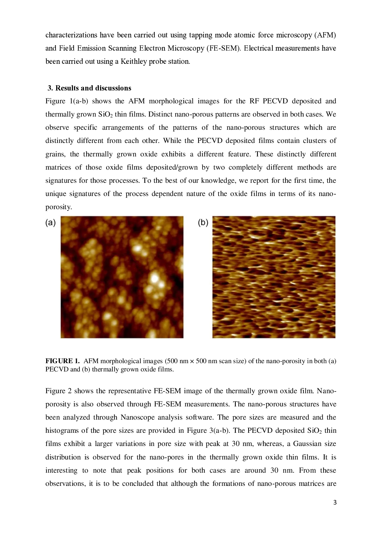
Nanoporosity in thin membranes and thin films is either an inherent property of the materials
or sometimes process dependent. Although, porosity is mostly undesirable in active devices,
there are several areas where nano-porous membranes or thin films are absolutely necessary.
As a matter of fact, each of the nano-pores inside a porous material has the potential to be an
active device if properly tuned by some means. It is still an open field of research the
communications between each of the nano-pores in nano-scale dimensions and their effect as
a whole in the bulk material. In recent times, nano-porous thin films have attracted much
research interests owing to their potential applications in fuel cells [1-6]; pressure and gas
sensors [7-8]. The utilization of nanoporous membranes in such devices require geometrically
controllable nanopores with controlled pore size and pore-density arrangements [6].
In the flexible electronics research, the most commonly used insulators are low temperature
plasma enhanced chemical vapor deposited (PECVD) silicon dioxide (SiO2) and silicon
nitrides (SiNx) [9]. There is a huge ongoing research on fabrication of low cost transparent
conductive oxide (TCO) films [10], which has applications in flexible displays, organic solar
cells, and organic light emitting diodes and so on [10-13]. Indium tin oxide (ITO) being one of
the major TCOs has drawback, like, high processing cost. Therefore, alternative solutions are
2
being researched to find out novel conductive oxide films. Silicon dioxide (SiO2) thin film is
one of the widely researched materials for several decades which have applications as the
dielectric interlayer in the microelectronic industries [14]; moisture permeation barriers [15];
optical coatings [16] and so on. Although this material has a huge prospect in the above
mentioned areas, the insulating nature of the oxide films does not allow their applications as
TCOs. Expensive chemical doping is required to obtain electrical conductivity in the SiO2 thin
films.
The aim of this present study is to characterize the nano-porosity of thermally grown and
PECVD deposited SiO2 thin films. The distinct arrangements of the nano-porous matrices in
those two processes show the signatures of growth/deposition methods. We also demonstrate a
simple low cost method to fabricate conductive nano-porous SiO2 thin films without any
intentional chemical doping. The conductive nanoporous oxide films have electrical resistivity
6 orders of magnitude lower compared to the insulating SiO2 films.
- Experimental details
2.1. Oxide growth in oxidation furnace and RF PECVD deposition
Thermally grown SiO2 thin films with thickness around 1 µm have been grown in oxidation
furnace at CEERI-Pilani with temperature ~1100 C. Dry-wet-dry oxidation cycles have been
used for total duration of ~3 hr on cleaned Si wafer substrates. For the RF PECVD deposition
of SiO2 thin films (thickness ~1µm) on cleaned Si wafer substrates, the working pressure and
substrate temperature have been fixed at 0.3 Torr and 300 C. We used an optimized recipe
for oxide deposition where the flow rates for the source gases were: 5 sccm (SiH4); 350 sccm
(N2O); 300 sccm (N2) and 170 sccm (Ar). The RF (13.56 MHz) power density has been fixed
at 155 mW/cm2. The optimized deposition rate (rd) was 50 nm/min.
2.2. Filling of nano-pores with metal
In order to obtain conducting oxide films, the
…(Full text truncated)…
This content is AI-processed based on ArXiv data.