On-Chip Implementation of Pipeline Digit-Slicing Multiplier-Less Butterfly for Fast Fourier Transform Architecture
The need for wireless communication has driven the communication systems to high performance. However, the main bottleneck that affects the communication capability is the Fast Fourier Transform (FFT), which is the core of most modulators. This study presents an on-chip implementation of pipeline digit-slicing multiplier-less butterfly for FFT structure. The approach is taken, in order to reduce computation complexity in the butterfly, digit-slicing multiplier-less single constant technique was utilized in the critical path of Radix-2 Decimation In Time (DIT) FFT structure. The proposed design focused on the trade-off between the speed and active silicon area for the chip implementation. The new architecture was investigated and simulated with MATLAB software. The Verilog HDL code in Xilinx ISE environment was derived to describe the FFT Butterfly functionality and was downloaded to Virtex II FPGA board. Consequently, the Virtex-II FG456 Proto board was used to implement and test the design on the real hardware. As a result, from the findings, the synthesis report indicates the maximum clock frequency of 549.75 MHz with the total equivalent gate count of 31,159 is a marked and significant improvement over Radix 2 FFT butterfly. In comparison with the conventional butterfly architecture, the design that can only run at a maximum clock frequency of 198.987 MHz and the conventional multiplier can only run at a maximum clock frequency of 220.160 MHz, the proposed system exhibits better results. The resulting maximum clock frequency increases by about 276.28% for the FFT butterfly and about 277.06% for the multiplier. It can be concluded that on-chip implementation of pipeline digit-slicing multiplier-less butterfly for FFT structure is an enabler in solving problems that affect communications capability in FFT and possesses huge potentials for future related works and research areas.
💡 Research Summary
The paper addresses the performance bottleneck posed by the Fast Fourier Transform (FFT) in modern wireless communication systems, focusing on the computationally intensive complex multiplication within the Radix‑2 Decimation‑In‑Time (DIT) butterfly. Traditional butterfly implementations rely on four real multipliers and two adders, which consume significant FPGA resources and limit the maximum operating frequency. To overcome this, the authors propose a multiplier‑less butterfly architecture that combines digit‑slicing with a single‑constant multiplier‑less (SCML) design and a pipelined data path.
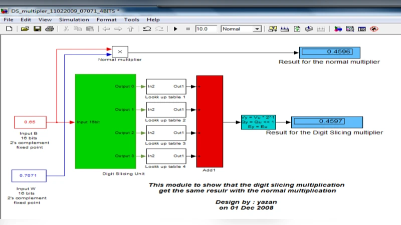
Digit‑slicing partitions each fixed‑point input word (e.g., 8‑bit two’s‑complement) into two 4‑bit blocks. For each block, the product with a known twiddle factor (the constant) is pre‑computed for all 16 possible values and stored in four small ROMs. During operation, the appropriate ROM entry is fetched and summed using simple adders, eliminating the need for any real multiplier. The SCML thus consists of four lookup tables and a lightweight adder network.
The butterfly is built by feeding the sliced inputs through the SCML, then combining the results with the other complex input using high‑speed parallel prefix adders (Kogge‑Stone and Stone‑Ling). Pipeline registers are inserted between stages, allowing each slice‑multiply and addition to complete within a single clock cycle, dramatically reducing critical‑path delay.
The design is described in Verilog HDL, synthesized with Xilinx ISE for a Virtex‑II XC2V500‑6FG456 FPGA. Synthesis reports show a total equivalent gate count of 31,159 and a maximum clock frequency of 549.75 MHz for the pipelined digit‑slicing multiplier‑less butterfly, and 609.98 MHz for the standalone SCML module. In contrast, a conventional butterfly using the FPGA’s built‑in multiplier reaches only 198.987 MHz, and a generic multiplier‑based design peaks at 220.160 MHz. Thus, the proposed architecture achieves roughly a 276 % increase in speed for the butterfly and a 277 % increase for the multiplier‑less unit, while also reducing silicon area.
Simulation results from MATLAB and ModelSim confirm functional correctness, and RTL schematics illustrate the pipeline stages and ROM‑based multiplier. Although power consumption is not quantified, the reduction in active multiplier circuitry suggests lower dynamic power.
The authors conclude that, when twiddle factors are known a priori (as in FFT), replacing multipliers with digit‑sliced ROM look‑ups yields substantial improvements in speed and area, making the approach attractive for high‑performance, low‑power DSP implementations on FPGAs. Future work is suggested in extending the method to variable‑precision or multi‑constant scenarios, performing detailed power analysis, and exploring ASIC realizations to further validate the architecture’s benefits.
Comments & Academic Discussion
Loading comments...
Leave a Comment