I2C Management Based on IPbus
CBM (Compressed Baryonic Matter) is mainly used to study QCD phase diagram of strong interactions in high and moderate temperature region. Before the next generation GBTx based CBM DAQ system is built up, the DPB (Data Processing Board) layer is used in data readout and data pre-processing, where a general FPGA FMC carrier board named AFCK is used. This paper mainly describes the management of the Inter-integrated Circuit (I2C) devices on AFCK and the FMCs it carries via IPBus, an FPGA-based slow control bus used in CBM DAQ system. On AFCK, the connection of IPBus depends on the correct initialization of a set of I2C devices, including the I2C-bus multiplexer (choosing correct I2C bus), the clock crosspoint switch (providing the 125MHz needed by 1000BASE-X/SGMII), the serial EEPROM with a EUI-48 address (providing the AFCK MAC address). An independent initial module can execute an I2C command sequence stored in a ROM, through which the FPGA can write to/read from the I2C devices without IPBus, so that the related I2C devices are correctly initialized and the necessary preparation for the IPBus start-up is fulfilled. After the initialization, a Wishbone I2C master core is used as an IPbus slave and all other I2C devices can be configured directly via IPBus. All the design has been fully tested in the CBM DPB design.
💡 Research Summary
The paper presents a complete solution for managing the I²C devices on the AFCK (AMC FMC Carrier Kintex) board and its attached FMC modules within the CBM (Compressed Baryonic Matter) data‑processing‑board (DPB) layer, using the IPBus slow‑control protocol. CBM’s DAQ architecture currently relies on a DPB layer that aggregates data from various detectors (MVD, STS, MUCH, RICH, TRD, TOF, PSD) before the next‑generation GBTx‑based system is deployed. The AFCK carrier hosts a set of essential I²C peripherals: a bus multiplexer, a clock cross‑point switch, a programmable crystal, an EEPROM containing a unique EUI‑48 MAC address, and system‑monitoring ICs. While IPBus can ultimately control all these devices, it itself depends on a few pre‑conditions: the correct I²C bus must be selected, a 125 MHz reference clock must be routed to the 1000BASE‑X/SGMII transceivers, and the MAC address must be read from EEPROM. Without these, the IPBus Ethernet link cannot be established.
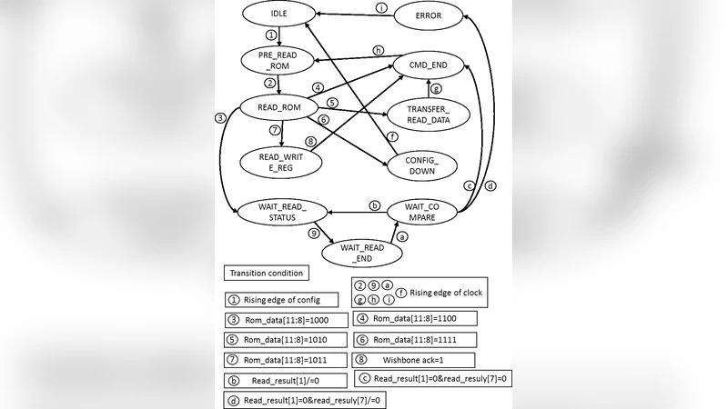
To meet this chicken‑and‑egg problem, the authors designed a two‑stage I²C management module. The first stage is an autonomous initialization block that activates on power‑up via an automatic reset. It contains a small ROM that stores a sequence of 16‑bit commands. Each command encodes (i) the I²C bus number (bits 15‑13), (ii) a read/write flag (bit 12), (iii) a register‑port identifier (bits 11‑8), and (iv) an 8‑bit data payload. A finite‑state‑machine (FSM) reads the ROM word by word, drives the I²C master core, and performs the required register accesses. The command set configures the bus multiplexer, programs the clock cross‑point switch to deliver the 125 MHz clock, and reads the EEPROM to obtain the board’s MAC address. After the ROM sequence finishes, the block automatically hands over control to the second stage.
The second stage is a Wishbone‑compatible I²C master core that is exposed as an IPBus slave. It provides four 8‑bit registers: a prescale register (sets SCL frequency), a control register (enables the core), a transmit/receive register (holds address, data, and command bytes), and a command/status register (issues I²C start/stop, read/write operations and reports completion). The IPBus software stack (available in C++ or Python) communicates over Ethernet, translates IPBus packets into Wishbone cycles, and reads/writes these registers, thereby allowing any I²C device on the board or on attached FMCs to be configured at run‑time.
The authors also discuss clock handling in detail. Before initialization, a separate crystal oscillator drives the I²C master’s SCL line. Once the cross‑point switch is programmed, the 125 MHz clock is routed to the FPGA’s system‑clock input and to the four high‑speed serial transceiver lanes, enabling 1 GbE/SGMII communication. The programmable crystal on the AFCK can be set to 156.25 MHz via I²C, and the same mechanism can configure crystals on FMC cards.
Experimental verification on the CBM DPB prototype showed that the autonomous initializer correctly set all required peripherals, after which the IPBus link came up without manual intervention. Subsequent IPBus commands were able to read and write arbitrary I²C registers, demonstrating real‑time configurability and monitoring. The dual‑module approach eliminates the need for manual pre‑configuration, improves system uptime, and provides a scalable framework that can be reused in the upcoming GBTx‑based DAQ system.
In conclusion, the paper delivers a robust hardware‑software co‑design that combines ROM‑based boot‑time I²C configuration with a Wishbone‑IPBus‑exposed I²C master, achieving reliable, online control of all I²C devices on the AFCK platform. This architecture satisfies the stringent requirements of high‑energy‑physics data acquisition while maintaining flexibility for future upgrades.
Comments & Academic Discussion
Loading comments...
Leave a Comment