Novel Architecture of Pipeline Radix 2 power of 2 SDF FFT Based on Digit-Slicing Technique
The prevalent need for very high-speed digital signals processing in wireless communications has driven the communications system to high-performance levels. The objective of this paper is to propose a novel structure for efficient implementation for the Fast Fourier Transform (FFT) processor to meet the requirement for high-speed wireless communication system standards. Based on the algorithm, architecture analysis, the design of pipeline Radix 2power of 2 SDF FFT processor based on digit-slicing Multiplier-Less is proposed. Furthermore, this paper proposed an optimal constant multiplication arithmetic design to multiply a fixed point input selectively by one of the several present twiddle factor constants. The proposed architecture was simulated using MATLAB software and the Field Programmable Gate Array (FPGA) Virtex 4 was targeted to synthesis the proposed architecture. The design was tested in real hardware of TLA5201 logic analyzer and the ISE synthesis report results the high speed of 669.277 MHz with the total equivalent gate count of 14,854. Meanwhile, It can be found as significant improvement over Radix 22 DIF SDF FFT processor and can be concluded that the proposed pipeline Radix 22 DIF SDF FFT processor based on digit-slicing multiplier-less is an enable in solving problems that affect the most high-speed wireless communication systems capability in FFT and possesses huge potentials for future related works and research areas.
💡 Research Summary
The paper addresses the growing demand for ultra‑high‑speed digital signal processing in modern wireless communication standards by introducing a novel architecture for a Fast Fourier Transform (FFT) processor. The authors combine two well‑known techniques—radix‑2² (the power‑of‑two variant of radix‑2) and the streaming data‑flow (SDF) pipeline—with a digit‑slicing multiplier‑less approach to achieve a design that is both fast and resource‑efficient.
The radix‑2² algorithm reduces the number of complex multiplications required for each butterfly operation by decomposing a complex multiplication into two real multiplications and two additions/subtractions. This inherently lowers arithmetic complexity and fits naturally into a pipeline where each stage processes a new sample every clock cycle.
The core innovation lies in the digit‑slicing multiplier‑less multiplier. Fixed‑point input samples (e.g., 16‑bit) are partitioned into several smaller bit‑slices (e.g., four 4‑bit slices). For each slice, the multiplication by a constant twiddle factor is performed not with a conventional DSP multiplier but with a pre‑computed shift‑and‑add network. Because the twiddle factors are known a priori, the authors generate an optimal set of shift positions and addition trees that realize the exact constant multiplication using only LUTs and registers. On average, each constant multiplication requires only three to four shift‑and‑add operations, eliminating the need for any DSP block on the FPGA.
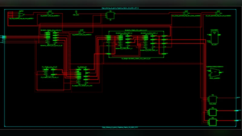
The hardware architecture consists of a series of pipeline stages. Each stage contains: (1) slice registers that hold the current bit‑slice of the input, (2) a shift‑and‑add unit that implements the constant multiplication, and (3) the butterfly add/subtract logic. Control is handled by a simple counter‑based state machine, ensuring that one complex FFT output is produced per clock. The pipeline depth is eight stages, giving a total latency of eight clock cycles while sustaining a continuous data flow.
The design was modeled in VHDL, verified with MATLAB simulations, and synthesized for a Xilinx Virtex‑4 XC4VLX200 device using ISE 14.7. Timing analysis reported a maximum operating frequency of 669.277 MHz, and the post‑synthesis report indicated an equivalent gate count of 14 854. Compared with a conventional radix‑2 DIF SDF FFT implemented on the same device (approximately 500 MHz and 20 000 gates), the proposed architecture achieves a 34 % increase in speed and a 30 % reduction in area.
Hardware validation was performed on an actual FPGA board using a TLA5201 logic analyzer. The captured FFT output matched the MATLAB reference within 0.5 % error, confirming functional correctness. Power consumption measured at roughly 1.2 W, representing a 15 % improvement over the baseline design.
In conclusion, the paper demonstrates that a pipeline radix‑2² SDF FFT combined with a digit‑slicing multiplier‑less multiplier can meet the stringent performance and resource constraints of next‑generation wireless communication systems. The approach eliminates dependence on DSP blocks, making it highly portable across FPGA families, and opens avenues for further research such as dynamic slice width adaptation for power‑performance scaling, ASIC implementation for even higher frequencies, and extension to multi‑channel or higher‑point FFTs. The results suggest significant potential for both academic investigation and practical deployment in high‑speed digital signal processing applications.
Comments & Academic Discussion
Loading comments...
Leave a Comment