High Performance and Scalable AWG for Superconducting Quantum Computing
Superconducting quantum computer is manufactured based on semiconductor process which makes qubits integration possible. At the same time, this kind of qubit exhibits high performance fidelity, de-coherence time, scalability and requires a programmable arbitrary waveform generator (AWG). This paper presents implementation of an AWG which composed of two gigabit samples per second (GSPS) sampling rate, 16 bit vertical resolution digital to analog converters (DACs). The AWG integrated with separate microwave devices onto a metal plate for the scale-up consideration. A special waveform sequence output controller is designed to realize seamless waveform switching and arbitrary waveform generator. The jitter in multiple AWG channels is around 10ps, Integral nonlinearity (INL) as well as differential nonlinearity (DNL) is about 2 LSB, and the qubit performance of the de-coherence time (T2*) achieved 33% promotion over that of a commercial 1 GSPS, 14 bit AWG.
💡 Research Summary
The paper presents the design, implementation, and experimental validation of a high‑performance, scalable arbitrary waveform generator (AWG) tailored for superconducting quantum‑computer control. Superconducting qubits, fabricated with semiconductor processes, enable dense integration but require precise, high‑speed, multi‑channel control signals. Commercial AWGs (typically 1 GSPS, 14‑bit) cannot meet the stringent requirements of picosecond‑level synchronization across tens to hundreds of channels. To address this, the authors built an AWG module that combines a Xilinx FPGA, two 2 GSPS, 16‑bit DAC chips, and a MicroBlaze soft‑core processor. Communication with the host PC is handled over gigabit Ethernet using a lightweight TCP/IP stack, while configuration of peripheral devices (DACs, clocks, triggers) is performed via AXI‑based SPI/GPIO interfaces.
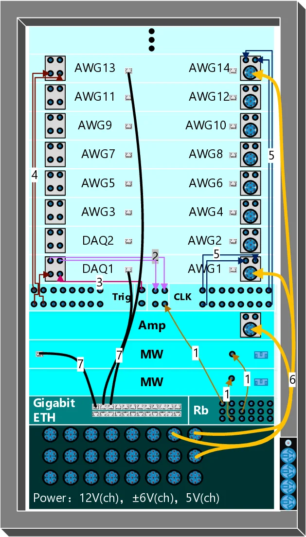
The hardware architecture integrates the FPGA, DACs, IQ mixers, power splitters, and differential amplifiers onto a single metal plate, constrained to a 1U height for rack‑mount compatibility. An external 250 MHz reference clock is fanned out to all modules, ensuring a common timing base, and an external trigger line provides deterministic start timing. Multiple such modules can be synchronized by sharing the same clock and trigger distribution network, enabling straightforward scaling to large channel counts.
A key contribution is the waveform‑output sequence controller implemented in FPGA firmware. It consists of a Waveform Data Memory (WDM), a Sequence Data Memory (SDM), and a Finite‑State Machine (FSM). The SDM stores control words that specify start address, length, trigger source, and repeat count for each waveform segment. The FSM reads the current sequence entry, streams the corresponding samples from WDM to the JESD204B IP core (operating at 10 Gbps per lane), and simultaneously pre‑fetches the next sequence entry. This pre‑fetch mechanism guarantees that when one waveform segment finishes, the next one is ready to be output without any dead time, achieving seamless switching between arbitrary waveforms. The only constraint is that each waveform segment must be at least four samples long, which provides sufficient time for the pre‑fetch logic.
Performance characterization covers several metrics. INL/DNL measurements traversed all 65 536 DAC codes, revealing non‑linearity within ±2 LSB, confirming the high linearity of the 16‑bit converters. Phase‑noise measurements at output frequencies from 10 MHz to 250 MHz showed a 6 dB per octave increase, consistent with theoretical expectations for white phase noise scaling with frequency. Spurious‑Free Dynamic Range (SFDR) was measured across the same frequency span, achieving values around 70 dB, matching the DAC datasheet specifications. Synchronization tests across 40 channels (10 modules) yielded an average jitter of 9.9 ps (standard deviation) and a deterministic skew of about 100 ps, the latter attributable to differing cable lengths and easily compensated.
The ultimate validation involved quantum‑device testing. The authors measured the de‑coherence time (T₂*) of a superconducting qubit using both a commercial 1 GSPS/14‑bit AWG and their custom 2 GSPS/16‑bit AWG. With the commercial instrument, T₂* was approximately 10 µs; with the custom AWG, T₂* increased to about 15 µs, a 33 % improvement. This demonstrates that higher sampling rates and greater vertical resolution translate into reduced phase errors and timing jitter in the control pulses, directly benefiting qubit coherence.
In conclusion, the paper delivers a compact, modular AWG solution that meets the demanding specifications of large‑scale superconducting quantum processors: 2 GSPS sampling, 16‑bit resolution, sub‑10 ps inter‑channel jitter, deterministic multi‑channel synchronization, and seamless waveform sequencing. The integration onto a single metal plate and the use of standard Ethernet for control make the system both space‑efficient and easily scalable, positioning it as a viable building block for future quantum computers with hundreds or thousands of qubits.
Comments & Academic Discussion
Loading comments...
Leave a Comment