Spectrally and Power Efficient Optical Communication Systems
Increased traffic demands globally and in particular in short-reach links in data centers will require optical communication systems to continue scaling at an accelerated pace. Nevertheless, energy constraints start to limit the bit rate that can be …
Authors: Jose Krause Perin
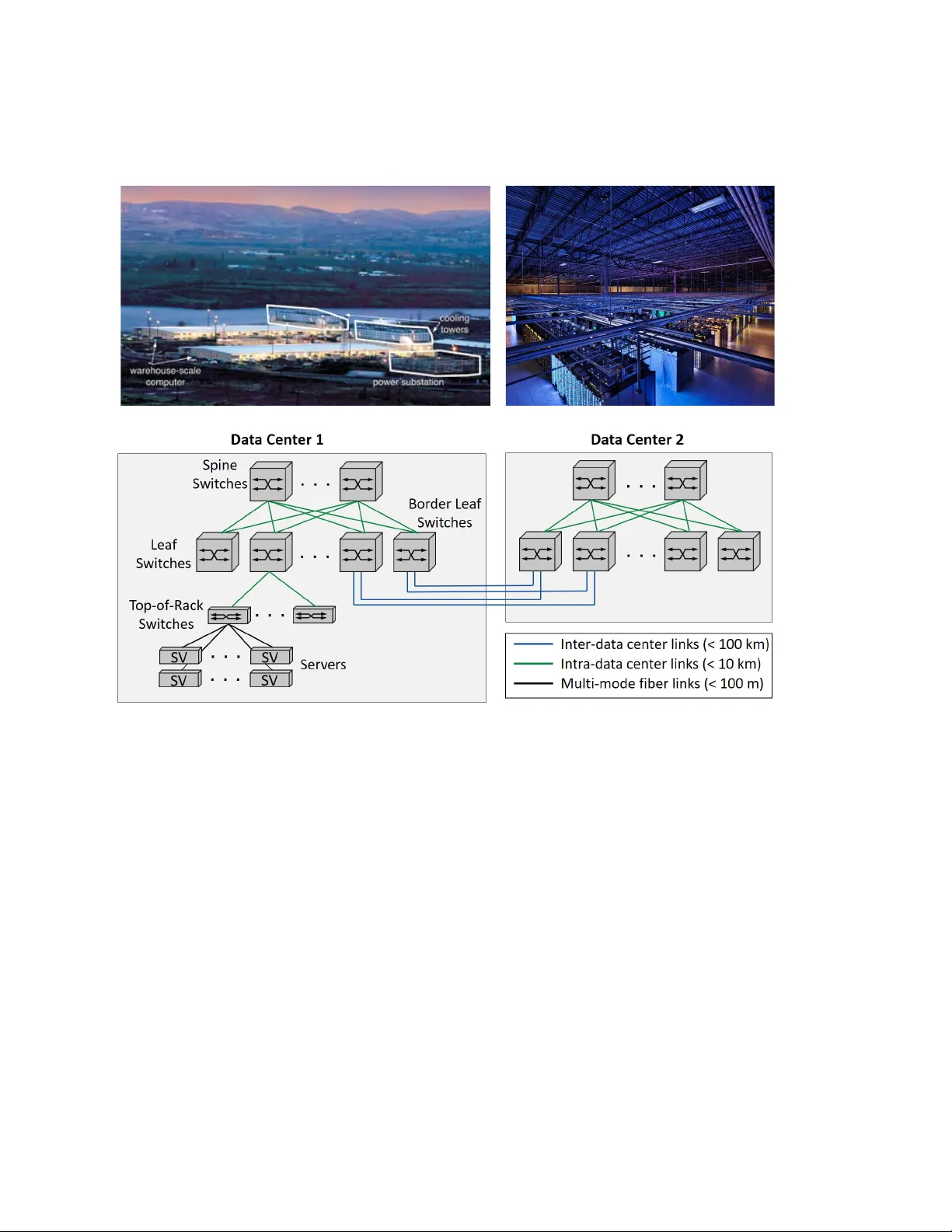
SPECTRALL Y AND PO WER EFFICIENT OPTICAL COMMUNICA TION SYSTEMS A DISSER T A TION SUBMITTED TO THE DEP AR TMENT OF ELECTRICAL ENGINEERING AND THE COMMITTEE ON GRADUA TE STUDIES OF ST ANF ORD UNIVERSITY IN P AR TIAL FULFILLMENT OF THE REQUIREMENTS F OR THE DEGREE OF DOCTOR OF PHILOSOPHY Jose Krause P erin June 2018 c Cop yrigh t b y Jose Krause P erin 2018 All Righ ts Reserv ed ii I certify that I ha ve read this dissertation and that, in m y opinion, it is fully adequate in scop e and qualit y as a dissertation for the degree of Do ctor of Philosophy . (Joseph M. Kahn) Principal Adviser I certify that I ha ve read this dissertation and that, in m y opinion, it is fully adequate in scop e and qualit y as a dissertation for the degree of Do ctor of Philosophy . (Ola v Solgaard) I certify that I ha ve read this dissertation and that, in m y opinion, it is fully adequate in scop e and qualit y as a dissertation for the degree of Do ctor of Philosophy . (Boris Murmann) Appro ved for the Stanford Univ ersit y Committee on Graduate Studies iii iv Abstract Increased traffic demands globally and in particular in short-reach links in data centers will require optical comm unication systems to contin ue scaling at an accelerated pace. Nev ertheless, energy constrain ts start to limit the bit rate that can b e practically transmitted ov er optical systems b oth at the shortest distances in data centers and at the longest distances in ultra-long submarine links. Short-reac h links in data cen ters face strict constrain ts on p o wer consumption, size, and cost, which will demand low-pow er solutions that scale to bit rates b eyond 100 Gbit/s p er wa v elength, while accommo dating increased losses due to longer fib er plant, m ultiplexing of more w av elengths, and p ossibly optical switching. A t the longest distances, submarine optical cables longer than ab out 5,000 km face energy constraints due to pow er feed limits at the shores, whic h restricts the electrical p ow er a v ailable to the undersea optical amplifiers, ultimately limiting the optical p ow er and throughput p er fib er. This dissertation addresses fundamental c hallenges tow ards designing sp ectrally and p ow er effi- cien t optical communication systems. The first part of this dissertation fo cuses on short-reach optical systems for intra- and in ter-data cen ter applications. Chapter 2 ev aluates higher-order mo dulation formats compatible with direct detection (DD) that are b est suited to replaced on/off keying (OOK) in next-generation data center links that supp ort 100 Gbit/s p er w av elength. W e show that four-level pulse-amplitude mo dulation (4-P AM) outp erforms orthogonal frequency-division m ultiplexing (OFDM) due to its relatively low complexity and higher tolerance to noise and distortion. And in fact, 4-P AM was later adopted by the IEEE 802.3bs task force to enable 400 Gbit/s using 8 × 50 Gbit/s and 4 × 100 Gbit/s transceivers. The w ork in Chapter 2 w as done in collab oration with Dr. Milad Sharif, who has conducted the research and analyses for single-carrier mo dulation formats. Chapter 3 fo cuses on how to impro ve the limited receiver sensitivit y of 4-P AM systems prop osed in Chapter 2 b y using av alanche photo dio des (APDs) or semiconductor optical amplifiers (SOAs). W e show ed that APDs and SOAs improv e the receiver sensitivity by 4 to 6 dB, which will extend the lifetime of 4-P AM and other DD-compatible mo dulation formats. The work in Chapter 3 was also done in collab oration with Dr. Milad Sharif, who studied the b enefits and drawbac ks of using v SO As. Chapter 4 fo cuses on the design of DSP-free coherent receiv er architectures for low-pow er short- reac h systems. As demonstrated in Chapters 2 and 3, DD-compatible formats face significant chal- lenges to scale b eyond 100 Gbit/s p er w a velength. Moreo ver, these systems already face tigh t practical constraints even when counting on amplification, either by using APDs or SO As. The underlying reason b ehind these challenges is that DD-compatible systems only leverage one degree of freedom of the optical channel, namely its intensit y . Coherent receivers allow four degrees of free- dom, tw o quadratures in tw o p olarizations. But coherent receiv ers hav e b een traditionally realized using high-sp eed analog-to-digital conv erters (ADCs) and digital signal pro cessing (DSP), which are prohibitiv ely p ow er hungry for data center applications. W e prop osed low-pow er coherent receivers arc hitectures that completely preclude the need of high-sp eed DSP and ADCs, while achieving simi- lar p erformance to their DSP-based counterparts. The work in Chapter 4 was done in collab oration with Dr. An ujit Shastri, who designed and simulated the p olarization recov ery system based on cascaded phase shifters and mak er tone detection. The second part of this dissertation fo cuses on ultra-long submarine optical links, where en- ergy constraints due to limited p o wer feed voltage at the shores ultimately limits the amount of information that can b e practically transmitted p er fib er. Chapter 5 fo cuses on the channel p ow er optimization of long-haul submarine systems limited b y energy constrain ts. The throughput of submarine transport cables is approac hing fundamental limits imp osed by amplifier noise and Kerr nonlinearity . Energy constraints in ultra-long submarine links exacerbate this problem, as the throughput p er fib er is further limited by the electrical p ow er a v ailable to the undersea optical amplifiers. Recen t w orks ha ve studied ho w emplo ying more spa- tial dimensions can mitigate these limitations. This chapter addresses the fundamen tal question of ho w to optimally use eac h spatial dimension. Sp ecifically , we discuss ho w to optimize the channel p o wer allo cation in order to maximize the information-theoretic capacity under an electrical p ow er constrain t. Our form ulation accoun ts for amplifier physics, Kerr nonlinearity , and p ow er feed con- strain ts. W e sho w that the optimized channel p ow er allo cation increases the capacity of submarine links b y ab out 70% compared to the theoretical capacity of a recently prop osed high-capacity sys- tem. Our solutions also provide new insights on the optimal num ber of spatial dimensions, amplifier op eration, and nonlinear regime op eration. Chapter 6 presen ts the concluding remarks of this dissertation and recommendations for future w ork. vi Ac kno wledgmen ts I am very grateful for the opp ortunit y of pursing my PhD at Stanford. I hav e learned a lot, gro wn a lot, and had the pleasure of w orking with man y truly brilliant p eople. Although a great part of the work as a graduate student is done alone, many p eople ha ve contributed along the wa y , and I w ould like to express my sincere gratitude to them. I w ould lik e to first thank m y principal adviser Prof. Joseph M. Kahn for his con tin uous supp ort, guidance, and encouragement o v er the past fiv e years. I hav e learned a lot from Prof. Kahn’s approac h to scientific research, from his commitment to teaching, and from his unw av ering pursuit of excellence. I could hav e not asked for a more insightful, generous, and caring research adviser. I w ould also lik e to thank members of my oral defense committee: Prof. Ola v Solgaard, Prof. Boris Murmann, Prof. Sanja y Lall, and Prof. Bernard Widro w, who generously agreed to be part of m y committee. I greatly appreciate their time and I am honored to hav e them in my oral defense committee. I wan t to thank Prof. Solgaard and Prof. Murmann for also serving as members of my dissertation reading committee and taking time out of their busy schedules to read this dissertation. I w ould also like to thank the Co ordena¸ c˜ ao de Ap erfei¸ coamento de Pessoal de N ´ ıv el Sup erior (CAPES) – a Brazilian federal gov ernmen t agency – for aw arding me a fellowship for three years of m y graduate studies. I would also lik e to thank the collab oration and funding from our industry partners: Maxim In tegrated, Go ogle, and Corning Inc. I am also very grateful for the con tinuous supp ort and guidance that I received from m y former professors at Univ ersidade F ederal do Esp ´ ırito Santo (UFES), in Brazil. In particular, Prof. Mois´ e s Rib eiro, who ov er the years has alwa ys demonstrated great in terest in m y p ersonal and academic success. I am also thankful for of all past and current mem b ers of Prof. Kahn’s Optical Communica- tions Group: Milad Sharif, Anujit Shastri, Sercan Arik, Daulet Ask arov, Ian Rob erts, Ruo Y u Gu, Karthik Choutagunta, Michael T aylor, Brandon Buscaino, Elaine Chou, and Hrishikesh Sriniv as. In particular, I would like to thank Milad Sharif and Anujit Shastri, who were my collab orators and greatly con tributed to part of the work in this dissertation. I am also v ery grateful for the man y friends I hav e made during my time at Stanford. Their vii friendship and supp ort made m y life at Stanford muc h more enjoy able. Last but certainly not least, I am also very grateful for my paren ts, Luiz F ernando and Elzina, and m y brother Luiz Carlos. Their man y selfless sacrifices allow ed me to b e where I am to day . And despite the distance, they never stopped supp orting and encouraging me. There are no words to describ e m y lov e and gratitude for them. viii Con ten ts Abstract v Ac kno wledgmen ts vii 1 In tro duction 1 1.1 Data center links . . . . . . . . . . . . . . . . . . . . . . . . . . . . . . . . . . . . . . 3 1.2 Long-haul submarine links . . . . . . . . . . . . . . . . . . . . . . . . . . . . . . . . . 5 I Data Cen ter Optical Systems 8 2 Data Center Links Beyond On/Off Keying 9 2.1 Optical fib er impairments . . . . . . . . . . . . . . . . . . . . . . . . . . . . . . . . . 10 2.2 Mo deling intra- and inter-data center links . . . . . . . . . . . . . . . . . . . . . . . . 14 2.3 Mo dulation formats compatible with direct detection . . . . . . . . . . . . . . . . . . 15 2.3.1 Pulse-amplitude mo dulation . . . . . . . . . . . . . . . . . . . . . . . . . . . . 15 2.3.2 Orthogonal frequency-division m ultiplexing or discrete multitone . . . . . . . 18 2.3.3 Single-sideband orthogonal frequency-division m ultiplexing . . . . . . . . . . 28 2.4 Performance comparison . . . . . . . . . . . . . . . . . . . . . . . . . . . . . . . . . . 31 2.5 Complexity comparison . . . . . . . . . . . . . . . . . . . . . . . . . . . . . . . . . . 33 2.6 Summary . . . . . . . . . . . . . . . . . . . . . . . . . . . . . . . . . . . . . . . . . . 35 3 Impro ving the Receiver Sensitivity of Data Center Links 37 3.1 Av alanc he photo dio des . . . . . . . . . . . . . . . . . . . . . . . . . . . . . . . . . . . 38 3.1.1 Shot noise . . . . . . . . . . . . . . . . . . . . . . . . . . . . . . . . . . . . . . 39 3.1.2 APD bandwidth and the gain-bandwidth pro duct . . . . . . . . . . . . . . . 41 3.2 System mo del for APD-based intra-data center links . . . . . . . . . . . . . . . . . . 43 3.2.1 P erformance ev aluation . . . . . . . . . . . . . . . . . . . . . . . . . . . . . . 44 3.3 WDM system p erformance . . . . . . . . . . . . . . . . . . . . . . . . . . . . . . . . . 46 ix 3.4 Practical considerations . . . . . . . . . . . . . . . . . . . . . . . . . . . . . . . . . . 48 3.5 Summary . . . . . . . . . . . . . . . . . . . . . . . . . . . . . . . . . . . . . . . . . . 48 4 Lo w-P o w er DSP-F ree Coherent Receivers 50 4.1 DSP-based coherent receiver (DP- M -QAM) . . . . . . . . . . . . . . . . . . . . . . . 52 4.2 DSP-free coherent receiver (DP-QPSK) . . . . . . . . . . . . . . . . . . . . . . . . . 55 4.2.1 P olarization demultiplexing . . . . . . . . . . . . . . . . . . . . . . . . . . . . 57 4.2.2 Carrier reco very . . . . . . . . . . . . . . . . . . . . . . . . . . . . . . . . . . 58 4.2.3 Prop osed startup proto col . . . . . . . . . . . . . . . . . . . . . . . . . . . . . 62 4.3 DSP-free differentially coherent (DP-DQPSK) . . . . . . . . . . . . . . . . . . . . . . 63 4.4 Performance comparison . . . . . . . . . . . . . . . . . . . . . . . . . . . . . . . . . . 65 4.5 Complexity comparison . . . . . . . . . . . . . . . . . . . . . . . . . . . . . . . . . . 66 4.6 Summary . . . . . . . . . . . . . . . . . . . . . . . . . . . . . . . . . . . . . . . . . . 69 I I Submarine Optical Systems 71 5 Maximizing the Capacity of Submarine Links 72 5.1 Problem formulation . . . . . . . . . . . . . . . . . . . . . . . . . . . . . . . . . . . . 73 5.1.1 Amplifier ph ysics . . . . . . . . . . . . . . . . . . . . . . . . . . . . . . . . . . 75 5.1.2 Kerr nonlinearit y . . . . . . . . . . . . . . . . . . . . . . . . . . . . . . . . . . 78 5.1.3 Optimization problem . . . . . . . . . . . . . . . . . . . . . . . . . . . . . . . 80 5.2 Results and discussion . . . . . . . . . . . . . . . . . . . . . . . . . . . . . . . . . . . 82 5.2.1 Channel p o wer optimization . . . . . . . . . . . . . . . . . . . . . . . . . . . . 82 5.2.2 Optimal n umber of spatial dimensions . . . . . . . . . . . . . . . . . . . . . . 87 5.2.3 Reco very from pump failure . . . . . . . . . . . . . . . . . . . . . . . . . . . . 88 5.3 Summary . . . . . . . . . . . . . . . . . . . . . . . . . . . . . . . . . . . . . . . . . . 89 6 Conclusions 90 A Deriv ation of the Gradient of the Channel Capacity 95 A.1 Gain Gradient . . . . . . . . . . . . . . . . . . . . . . . . . . . . . . . . . . . . . . . 96 A.1.1 Gain deriv ative with resp ect to EDF length . . . . . . . . . . . . . . . . . . . 97 A.2 SNR gradient . . . . . . . . . . . . . . . . . . . . . . . . . . . . . . . . . . . . . . . . 98 A.3 Spectral efficiency gradien t . . . . . . . . . . . . . . . . . . . . . . . . . . . . . . . . 99 A.3.1 Sp ectral efficiency gradient deriv ative with resp ect to EDF length . . . . . . 99 Bibliograph y 101 x List of T ables 2.1 Parameters used in Monte Carlo simulations for determining receiver sensitivity and OSNR required of DD-compatible mo dulation sc hemes. . . . . . . . . . . . . . . . . 33 2.2 Complexity comparison of DD-compatible mo dulation formats. . . . . . . . . . . . . 34 3.1 Characteristics of published APDs. . . . . . . . . . . . . . . . . . . . . . . . . . . . . 39 3.2 Simulation parameters for Monte Carlo simulation of APD-based system. . . . . . . 48 4.1 Impairments and constraints for intra- and inter-data center links. . . . . . . . . . . 51 4.2 Up date equations using CMA or LMS algorithm for the simplified p olarization de- m ultiplexer. . . . . . . . . . . . . . . . . . . . . . . . . . . . . . . . . . . . . . . . . . 53 4.3 Coherent and differentially coheren t systems simulation parameters. Monte Carlo sim ulations used 2 17 sym b ols. . . . . . . . . . . . . . . . . . . . . . . . . . . . . . . . 67 4.4 Complexity comparison of mo dulation schemes allowing more than one degree of freedom of the optical c hannel. . . . . . . . . . . . . . . . . . . . . . . . . . . . . . . 68 5.1 Parameters of submarine system considered in the optimization. . . . . . . . . . . . 82 xi List of Figures 1.1 Global IP traffic forecast. A zettabyte equals 10 21 b ytes. Source: Cisco Global IP T raffic Growth, 2016–2021. . . . . . . . . . . . . . . . . . . . . . . . . . . . . . . . . 2 1.2 (a) Global IP traffic growth in data centers. (b) Pro jected traffic by destination in 2021. Ab out 71% of all traffic is exp ected to reside within data cen ters. Source: Cisco Global Cloud Index, 2016–2021. . . . . . . . . . . . . . . . . . . . . . . . . . . . . . . 2 1.3 (a) hyperscale data center, (b) server racks inside a data center, and (c) typical tw o- tier top ology allo wing connectivity b etw een neighboring data centers. . . . . . . . . . 4 1.4 Map of deploy ed submarine cables. White no des represent landing p oints, and cable color is to ease visualization. Source: www.submarinecablemap.com/. . . . . . . . . 5 1.5 (a) Cross-section of a mo dern submarine cable, as describ ed in US P atent No. 4,278,835 (Source: Wikimedia), and (b) TE SubCom submarine repeater, i.e., an EDF A for sub- marine optical links. . . . . . . . . . . . . . . . . . . . . . . . . . . . . . . . . . . . . 6 2.1 Example of 100 Gbit/s transceiver based on 4 × 25 Gbit/s for intra-data cen ter links up to 2 km of SMF. The mo dule size is 18.4 mm × 50 mm × 8.5 mm with p ow er consumption of roughly 4 W. Images courtesy of Junip er Netw orks and Oclaro. . . . 10 2.2 Atten uation (top) and disp ersion (b ottom) co efficien ts of standard SMF (SMF28). . 11 2.3 Small-signal fib er frequency resp onse for (a) α = 0 and (b) α = 1. . . . . . . . . . . . 12 2.4 F requency of first notch of IM-DD channel frequency resp onse for several v alues of c hirp parameter. . . . . . . . . . . . . . . . . . . . . . . . . . . . . . . . . . . . . . . 13 2.5 System-level diagrams of (a) intra-data center links and (b) inter-data center links. . 14 2.6 Example of optimized levels and their corresp onding noise conditional probability densit y functions. . . . . . . . . . . . . . . . . . . . . . . . . . . . . . . . . . . . . . . 17 2.7 Blo ck diagram of the OFDM transmitter for DC- and ACO-OFDM. Example time- domain w av eforms are shown on the right. . . . . . . . . . . . . . . . . . . . . . . . . 19 2.8 Comparison b et ween bit loading (left) and pow er allo cation (righ t) done b y the Levin- Camp ello and conv entional water filling algorithms. B n refers to the num b er of bits in eac h sub carrier. Hence, the constellation size is 2 B n . . . . . . . . . . . . . . . . . . 22 xii 2.9 Comparison b etw een (a) preempahsis and (b) Levin-Camp ello algorithm for p ow er allo cation and bit loading. Figures show pow er sp ectrum (left) and bit loading (righ t) at the transmitter (top) and receiver (b ottom). The acronym CS stands for the QAM constellation size. . . . . . . . . . . . . . . . . . . . . . . . . . . . . . . . . . . . . . . 23 2.10 Clipping and quantization noise v ariance normalized b y the signal p ow er σ 2 as a function of clipping ratio for DC-OFDM. . . . . . . . . . . . . . . . . . . . . . . . . . 25 2.11 SNR as a function of the receiv ed p o wer including and disregarding quantization noise. These curves were obtained for ENOB = 6, and other parameters as given in T able 2.1. 27 2.12 Required ENOB to achiev e target BER of 1 . 8 × 10 − 4 for DC-OFDM (dashed lines) and A CO-OFDM (solid lines) with 16- and 64-QAM nominal constellation sizes. . . 28 2.13 Blo ck diagram of SSB-OFDM transmitter. Output electric field consists of a SSB- OFDM signal plus a strong unmo dulated carrier. . . . . . . . . . . . . . . . . . . . . 29 2.14 Performance comparison of DD-compatible m odulation sc hemes vs chromatic disp er- sion at 112 Gbit/s. . . . . . . . . . . . . . . . . . . . . . . . . . . . . . . . . . . . . . 32 2.15 Coarse estimate of p ow er consumption of high-sp eed DA Cs, ADCs, and DSP for v arious DD-compatible mo dulation schemes at 100 Gbit/s. . . . . . . . . . . . . . . . 35 3.1 Photo detection in a con ven tional PIN photo detector and in an APD. Source: Bahaa Saleh et al. “F undamentals of Photonics,” 1991. . . . . . . . . . . . . . . . . . . . . 38 3.2 Examples of APD structures. . . . . . . . . . . . . . . . . . . . . . . . . . . . . . . . 40 3.3 Bandwidth-vs-gain curv e for differen t APDs illustrating the tw o regimes of op erations: lo w-gain op eration where bandwidth is limited by transit-time and R C time constan ts, and high-gain op eration where gain is limited b y av alanche buildup time given rise to a fixed gain-bandwidth pro duct. . . . . . . . . . . . . . . . . . . . . . . . . . . . . . 42 3.4 Blo ck diagram for APD-based system. . . . . . . . . . . . . . . . . . . . . . . . . . . 43 3.5 Equiv alen t baseband blo ck diagram for APD-based receiver. . . . . . . . . . . . . . . 44 3.6 Receiver sensitivity improv ement versus APD gain for 4-P AM and k A = 0 . 1 (Si) and k A = 0 . 2 (InAlAs) and t w o v alues of GBP: 100 GHz and 300 GHz. The 8-P AM b est-case scenario of GBP = 300 GHz and k A = 0 . 1 is shown for referenc e. Results assume parameters from T able 3.2. . . . . . . . . . . . . . . . . . . . . . . . . . . . . 45 3.7 Receiver sensitivity improv emen t versus fib er length for 4-P AM. . . . . . . . . . . . . 47 4.1 Blo ck diagram of a DSP-based coherent receiver. . . . . . . . . . . . . . . . . . . . . 52 4.2 Blo ck diagram of (a) CD and 2 × 2 MIMO equalizers used in conv en tional coherent receiv ers, and (b) simplified equalizer for short-reach applications assuming sm all-CD and small-DGD appro ximation. . . . . . . . . . . . . . . . . . . . . . . . . . . . . . . 53 4.3 Blo ck diagram of DP-QPSK receiver based on analog signal pro cessing. . . . . . . . 55 4.4 Blo ck diagram of carrier recov ery based on (a) OPLL and (b) EPLL. . . . . . . . . . 56 xiii 4.5 Schematic diagram of p olarization recov ery . . . . . . . . . . . . . . . . . . . . . . . . 58 4.6 Blo ck diagram of carrier phase estimators for QPSK inputs based on (a) Costas lo op and (b) a multiplier-free approach based on XORs. LIA denotes limiting amplifier, and ABS denotes full-wa ve rectifier. Though not explicitly sho wn, the comparator ma y b e clo ck ed in order to facilitate circuit design. . . . . . . . . . . . . . . . . . . . 59 4.7 Equiv alen t blo ck diagram for Costas lo op, without sign op eration sgn( · ), and X OR- based lo op including sgn( · ). . . . . . . . . . . . . . . . . . . . . . . . . . . . . . . . . 60 4.8 Maximum loop dela y for 0.5-dB SNR p enalty as a function of the combined linewidth. Curv es are sho wn for lo op natural frequency optimized at every p oint, and when lo op natural frequency is t wice the optimal. . . . . . . . . . . . . . . . . . . . . . . . . . . 61 4.9 Comparison of SNR p enalty vs com bined linewidth for Costas lo op and XOR-based lo op. Sim ulation curves include thermal noise and ISI p enalties, while theory curves do not. . . . . . . . . . . . . . . . . . . . . . . . . . . . . . . . . . . . . . . . . . . . . 62 4.10 Blo ck diagrams of differentially coherent detection metho ds (a) with a lo cal osc illator and (b) without a lo cal oscillator. The inputs to the differentially coherent detection metho d in (a) are XI and XQ from Fig. 4.3. Optical dela y interferometers are used for (b). . . . . . . . . . . . . . . . . . . . . . . . . . . . . . . . . . . . . . . . . . . . . 63 4.11 SNR p enalty as a function of frequency offset b etw een transmitter and LO lasers for a 224 Gbit/s DP-DPQSK system. . . . . . . . . . . . . . . . . . . . . . . . . . . . . . 64 4.12 Comparison of p erformance of coherent detection schemes vs. disp ersion at 224 Gbit/s. Unamplified systems are characterized in terms of (a) receiv er sensitivity , while amplified systems are characterized in terms of (b) OSNR required. The x -axis ma y b e in terpreted as total disp ersion in intra-data cen ter links or residual disp ersion after optical CD comp ensation in inter-data center links similarly to the resultin in Chapter 2. . . . . . . . . . . . . . . . . . . . . . . . . . . . . . . . . . . . . . . . . . . 66 4.13 Coarse estimate of p ow er consumption of high-sp eed DA Cs, ADCs, and DSP for v arious mo dulation schemes at 200 Gbit/s. . . . . . . . . . . . . . . . . . . . . . . . 68 5.1 Equiv alen t blo ck diagram of each spatial dimension of submarine optical link including amplifier noise and nonlinear noise. . . . . . . . . . . . . . . . . . . . . . . . . . . . . 73 5.2 Absorption and gain co efficients for the EDF used in simulations. . . . . . . . . . . . 76 5.3 Comparison b etw een experiment and theory for gain and ASE p ow er in 0.1 nm for differen t v alues of pump p ow er. . . . . . . . . . . . . . . . . . . . . . . . . . . . . . . 77 5.4 Nonlinear co efficien ts for (top) 50 km of standard SMF, and (b ottom) 50 km of large- effectiv e-area fib er used in ultra-long haul optical communications. . . . . . . . . . . 79 xiv 5.5 Optimized pow er allo cation P n for several v alues of pump pow er P p . Kerr nonlinearit y is disregarded in (a) and included in (b). Their corresp onding achiev able sp ectral efficiency is sho wn in (c) and (d). Note that P n corresp onds to the input p ow er to the amplifier. The launc hed p ow er is ˜ P n = G ( λ n ) F ( λ n ) P n = A ( λ n ) P n . Th us, the launc h p ow er is 9.75 dB ab ov e the v alues shown in these graphs. . . . . . . . . . . . 83 5.6 Theoretical (a) amplifier gain, (b) ideal GFF gain, and (c) accumulated ASE p ow er in 50 GHz after 1, 100, 200, and 287 spans of 50 km. . . . . . . . . . . . . . . . . . . 84 5.7 (a) T otal capacit y p er single-mo de fib er as a function of pump p ow er. (b) Ratio b et ween ASE and nonlinear noise p ow er for the optimization in (a). . . . . . . . . . 86 5.8 T otal capacity p er spatial dimension as a function of span length for a fixed p ow er budget. ASE only and ASE + Kerr nonlinearity curves ov erlap, as av ailable p ow er budget restricts op eration to the linear regime. . . . . . . . . . . . . . . . . . . . . . 87 5.9 Capacity as a function of the num b er of spatial dimensions for the system of T able 5.1 assuming a p o wer budget of P = 2 . 5 kW for all amplifiers. . . . . . . . . . . . . . . . 88 5.10 Difference in signal p o wer with resp ect to correct p ow er allocation in the even t of a single pump failure at the span indexed by zero. After ab out tw o spans the p ow er lev els are restored to their correct v alues. . . . . . . . . . . . . . . . . . . . . . . . . 88 xv xvi Chapter 1 In tro duction One of the pillars supp orting the information age is the ability to transmit ever-larger amounts of information across countries and con tinents. Optical communication systems hav e b een remark ably successful in fulfilling that task. Over the past three decades, pivotal technologies such as erbium- dop ed fib er amplifiers (EDF As), wa velength-division m ultiplexing (WDM), and coherent detection emplo ying digital comp ensation of fib er impairments hav e enabled data transmission of tens of terabits p er second across transo ceanic distances. Ov er the next few years, traffic demands are exp ected to contin ue growing at an accelerated pace. According to the Cisco forecast shown in Fig. 1.1, global Internet proto col (IP) traffic has approac hed 1 zettab yte (10 21 b ytes) p er y ear in 2016, and it is exp ected to gro w at a comp ound ann ual rate of 24%, resulting in roughly a three-fold increase in traffic ov er fiver years. Meeting this pro jected traffic gro wth will b e particularly challenging at the shortest distances, as shifting computing paradigms ha ve transformed ho w information is distributed, pro cessed, and stored. F or instance, web-based applications, con tent streaming, and cloud computing hav e turned p ersonal computers and mobile devices in to “mere” clien t interfaces, while most of the computing hea vy lifting is realized remotely in large computing facilities known as data centers. As a result, o verall traffic and growth rate is ev en larger in short-reach optical links within data centers. As shown in Fig. 1.2a, IP traffic is already ab ov e 10 zettabytes (greater than Fig. 1.1), and it is exp ected to gro w at a comp ound annual rate of 25%, resulting in a three-fold increase ov er five years. Fig. 1.2b illustrates the pro jected traffic distribution by destination in 2021. Ab out 71% of the global data center IP traffic is exp ected to reside within data centers, while user-destined traffic will account for only 14%. The remaining 15% will b e b etw een data centers. This trend will b e accen tuated by mac hine learning applications, whereby the end user makes simple queries that, nev ertheless, require significant computing p ow er. As traffic demands con tin ue to soar globally and in particular in data cen ters, optical commu- nication systems m ust contin ue to scale at an accelerated pace. How ev er, energy constraints start 1 2 CHAPTER 1. INTR ODUCTION 2016 2017 2018 2019 2020 2021 1 . 2 1 . 5 1 . 8 2 . 2 2 . 7 3 . 3 In ternet traffic (Zettabyte/y ear) Figure 1.1: Global IP traffic forecast. A zettab yte equals 10 21 b ytes. Source: Cisco Global IP T raffic Gro wth, 2016–2021. 2016 2017 2018 2019 2020 2021 6 . 8 9 . 1 11 . 6 14 . 1 17 . 1 20 . 6 In ternet traffic (Zettabyte/y ear) Within data center Data center to data center Data center to user 71% 15% 14% Pro jected traffic by destination in 2021 (a) (b) Figure 1.2: (a) Global IP traffic gro wth in data cen ters. (b) Pro jected traffic by destination in 2021. Ab out 71% of all traffic is expected to reside within data cen ters. Source: Cisco Global Cloud Index, 2016–2021. to limit the bit rate that can b e practically transmitted o ver those systems b oth at the shortest distances and at the longest distances [1]. At the shortest distances, optical systems for data centers face strict constrain ts on p ow er consumption, size, and cost, factors that w ere usually secondary in designing high-p erformance optical systems. At the longest distances, submarine optical cables longer than ab out 5,000 km face energy constrain ts due to p ow er feed limits at the shores, which restricts the electrical p ow er av ailable to the undersea optical amplifiers, ultimately limiting the optical p o wer and throughput p er fib er. In this dissertation, we prop ose sp ectrally and p ow er efficient optical systems for short-reach links in data centers and ultra-long links in submarine systems. Given the evident differences in 1.1. D A T A CENTER LINKS 3 those systems, differen t strategies are warran ted. In data center applications, w e prop ose lo w-p ow er coheren t detection systems that completely av oid high-sp eed analog-to-digital conv erters (ADC) and digital signal pro cessors (DSP). At the longest distances, we optimize the channel p ow er allo cation to maximize the information-theoretic capacit y p er fib er under an electrical p ow er constraint. The subsequent subsections detail the problems faced in data centers and submarine systems and review part of the terminology and tec hnicalities of each problem. 1.1 Data center links Fig. 1.3a shows an exemplary data center, and Fig. 1.3b displays the interior of a large data center con taining numerous rows of computer clusters. Hyper-scale data centers to da y can accommo date o ver 100,000 serv ers. These systems are t ypically interconnected follo wing a tw o-tier top ology [2], as illustrated in Fig. 1.3c. In this configuration all servers in a rack connect to top-of-the-rack switches that are connected to leaf switches, whic h in turn connect to every spine switch. In some cases, neigh b oring data centers may b e interconnected by connecting their leaf switches. The short links of a few hundred meters, shown in black in Fig. 1.3c, typically use vertical-ca vit y surface-emitting lasers (VCSEL) with multi-mode fib er (MMF) due to low manufacturing costs, low p o wer consumption, and ease of coupling light in to the fib er, while other links in the data center use single-mo de fib ers (SMF), whic h allow transmission ov er longer distances. Throughout this dissertation, we will refer to intra-data center links as the SMF links reaching up to 10 km that connect different switches in a data center, shown in green in Fig. 1.3c. In ter-data cen ter links reaching up to 100 km connect switches of neigh b oring data centers and are shown in blue in Fig. 1.3c. In to day’s data cen ters these links are realized by multiplexing sev eral wa v elengths carrying con ven tional on/off keying (OOK) mo dulated signals. F or instance, 100 Gbit/s links are ac hiev ed b y m ultiplexing four wa v elengths, each carrying 25 Gbit/s OOK signals. The IP traffic forecast sho wn in Fig. 1.1 suggests that data center links will need to scale to higher bit rates p er wa v elength. In fact, one of the industry goals w as to develop transceiv ers capable of transmitting 100 Gbit/s per w av elength. How ever, in addition to higher throughput p er w av elength, next-generation transceiv ers will likely need to tolerate higher fib er losses due to longer fib er plant, reduced p ow er p er c hannel in order to accommo date more wa velengths while complying with eye safety regulations, and p ossibly optical switc hes that will complement p ow er-hungry electronic switc hes. Therefore, the c hallenge of next-generation optical systems for data center is to supp ort higher bit rates p er wa velength, while offering reasonable p o wer margin. T o satisfy strict constraints in p o wer consumption and cost, research fo cused initially on mo du- lation formats compatible with direct detection, i.e., detection of information enco ded in the optical in tensity . How ever, Chapters 2 and 3 show that these direct-detected (DD) systems are extremely 4 CHAPTER 1. INTR ODUCTION (a) (b) (c) Figure 1.3: (a) h yp erscale data center, (b) server racks inside a data center, and (c) typical tw o-tier top ology allo wing connectivity b etw een neighboring data centers. constrained b eyond 100 Gbit/s, and in the long term, they likely cannot offer satisfactory p ow er margin even when lev eraging optical amplification or a v alanche photodio des. The underlying reason b ehind these challenges is that DD-compatible systems only leverage one degree of freedom of the optical channel, namely its in tensit y . Coherent detection enables four degrees of freedom of SMF, namely t wo quadratures in tw o p olarizations, and impro v es noise tolerance by up to 20 dB b y mixing a weak signal with a strong lo cal oscillator. Nevertheless, commercial coherent transceivers to day require high-sp eed ADCs and DSP , making them prohibitiv ely p ow er-hungry and costly for data cen ters applications. T o address these challenges, in Chapter 4, w e detail lo w-p o wer DSP-free co- heren t and differentially coherent arc hitectures that allow high-sp ectral efficiency and p erformance comparable to their DSP-based coun terparts, while consuming muc h less p ow er. 1.2. LONG-HA UL SUBMARINE LINKS 5 Figure 1.4: Map of deploy ed submarine cables. White no des represent landing p oints, and cable color is to ease visualization. Source: www.submarinecablemap.com/. 1.2 Long-haul submarine links As evidenced by a recent surge in deploymen t, submarine systems are of great and increasing im- p ortance to so ciety and information tec hnology . On Octob er 7, 2017, The Economist rep orted that 100,000 km of submarine cable was laid in 2016, up from 16,000 km in 2015. This is consistent with the $ 9.2-billion in vestmen t on submarine links b etw een 2016 and 2018, five times as muc h as in the previous three y ears. Fig. 1.4 sho ws a w orld map of deplo yed undersea optical communication cables. The white no des represen t cable landing p oints. T rans-atlan tic cables connecting the United States (US) to Europ e reac h ov er 6,000 km, while trans-pacific cables connecting the US to Asia reach ov er 11,000 km, whic h is roughly the same length of cables connecting the US to the coast of Brazil. The submerged cables and other equipment are reinforced to supp ort the water pressure at the sea b ed, and they are designed to op erate uninterruptedly for 25 years. Fig. 1.5a sho ws a cross- section of a mo dern submarine cable. T o compensate for the optical fib er atten uation of roughly 0.16 dB/km for state-of-the-art SMFs, optical rep eaters are p erio dically p ositioned every ∼ 50 km. A submarine-grade rep eater is show in Fig. 1.5b. These rep eaters are p o wered from the shores, where the dielectric constant of cables limits the feed voltages to 12–15 kV. Hence, the p ow er av ailable to eac h rep eater is limited. 6 CHAPTER 1. INTR ODUCTION (a) (b) Figure 1.5: (a) Cross-section of a mo dern submarine cable, as describ ed in US Paten t No. 4,278,835 (Source: Wikimedia), and (b) TE SubCom submarine rep eater, i.e., an EDF A for submarine optical links. T o illustrate the effect of this limitation, let us consider the example of a 10,000-km-long cable, whic h is typical of cables connecting the US to Asia or to Brazil. Assuming that amplifiers are p ositioned every 50 km results in a total of 200 amplifiers. All these amplifiers are p o wered from the shores where the feed voltage is 12 kV. F or maximum electrical p ow er transfer, the source resistance (cables) must b e equal to the load resistance (rep eaters). Therefore, the energy dissipated in the cables must b e equal to the energy av ailable to the rep eaters. Assuming cable resistance of ∼ 1Ω / km, leads to 3,600 W of p ow er for all rep eaters, or equiv alently 18 W for each of the 200 rep eaters. T ypically , 10% of the rep eater p ow er is sp ent in op erations that do no contribute directly to optical amplification such as co oling and monitoring [3]. Therefore, 16.2 W is a v ailable for amplification. Assuming that the cable contains eight fib er pairs. The EDF A for each fib er would hav e roughly 1 W of electrical p ow er. Unfortunately , EDF As are not remark ably p ow er efficien t; typical electric- to-optical p o wer conv ersion efficiency ranges from 1 . 5% to 5% [3, 4]. Thus, 5% efficiency results in appro ximately 17 dBm of av ailable optical p ow er at the output of each amplifier. As a result, from all the electrical p ow er fed to the cable, only roughly 2% b ecomes useful optical p o wer. This limit in optical p o wer naturally p oses a strict limit in the throughput p er fib er. T o mitigate this problem, recent works hav e turned to an insigh t from Shannon’s capacity that establishes that in energy-constrained systems, we can maximize capacity by employing more di- mensions while transmitting less data (p ow er) in each. In fact, recent works ha v e studied how emplo ying more spatial dimensions (mo des, cores, or fib ers) through spatial-division multiplexing (SDM) improv es capacity and p ow er efficiency of submarine systems [3, 5–7]. In complement to that w ork, w e address the fundamental question of ho w to optimally use each spatial dimension under an energy constraint. Sp ecifically , in Chapter 5, w e demonstrate how to optimize the optical p ow er of eac h WDM channel in order to maximize the information-theoretic capacity p er spatial dimension 1.2. LONG-HA UL SUBMARINE LINKS 7 giv en a constrain t in the total electrical p ow er. Our formulation accoun ts for amplifier physics, Kerr nonlinearit y , and p ow er feed constrain ts. Modeling amplifier physics is critical for translating en- ergy constraints into parameters that gov ern the channel capacity such as amplification bandwidth, noise, and optical p ow er. W e sho w that the optimized c hannel p ow er allo cation almost doubles the capacit y of submarine links compared to recen tly published w orks lev eraging SDM. Our solutions also provide new insights on the optimal num b er of spatial dimensions, amplifier op eration, and nonlinear regime op eration. In the second part of this dissertation, C hapter 5 form ulates the problem of optimizing the pow er allo cation under an energy constraint. Chapter 5 also details the mo dels used for amplifier physics, Kerr nonlinearity , as w ell as the optimization algorithms used to solve the resulting non-conv ex problem. P art I Data Cen ter Optical Systems 8 Chapter 2 Data Cen ter Links Bey ond On/Off Keying Scaling the capacity of data center links has long relied on using m ultiple wa velengths or multiple fib ers to carry con v entional on-off k eying (OOK) signals. Curren t 100 Gbit/s transceiv ers, for instance, use either ten multi-mode fib ers (MMFs) each carrying 10 Gbit/s OOK signals, or four w av elengths of 25 Gbit/s OOK in one single-mo de fib er (SMF), which is the case of the mo dule sho wn in Fig. 2.1. This strategy cannot scale m uch further, how ev er, as 400 Gbit/s links, for instance, w ould require 16 lanes of 25 Gbit/s, resulting in prohibitively high cost, size, and p o w er consumption. Recent researc h has fo cused on sp ectrally efficient mo dulation formats compatible with direct detection (DD) [8–11] to enable 100 Gbit/s p er wa v elength. These “single-laser 100 G links” are in tended to minimize optical comp onen t count, pow er consumption and size [12], and may facilitate optical switc hing in future data center netw orks. Sev eral mo dulation formats ha v e b een prop osed to realize single-laser 100 G links, including pulse- amplitude mo dulation (P AM) [13, 14], carrierless amplitude-and-phase (CAP) [14, 15], quadrature amplitude mo dulation (QAM) [16], orthogonal multi-pulse mo dulation (OMM) [17], and orthogonal frequency-division multiplexing (OFDM), often referred to as discrete multi-tone (DMT) [14, 18]. All attempt to provide higher sp ectral efficiency than OOK, while offering similar complexity and p o wer consumption. In this chapter, we review and compare the most promising mo dulation formats to enable single- laser 100G links. As a complement to prior simulation-based studies, we derive analytical mo dels to ev aluate p erformance and complexity of different mo dulation formats, since analysis is more generally applicable and fosters insight into design optimization and the relativ e merits of the v arious schemes. In Section 2.1, we start by reviewing the main impairmen ts of the optical fib er in short-reac h links. In Section 2.2, we review important c haracteristics of intr a- and inter-data cen ter links. In Section 2.3, 9 10 CHAPTER 2. D A T A CENTER LINKS BEYOND ON/OFF KEYING Figure 2.1: Example of 100 Gbit/s transceiver based on 4 × 25 Gbit/s for in tra-data center links up to 2 km of SMF. The mo dule size is 18.4 mm × 50 mm × 8.5 mm with p ow er consumption of roughly 4 W. Images courtesy of Junip er Net works and Oclaro. w e discuss mo dulation formats compatible with direct detection fo cusing primarily on multicarrier formats based on OFDM. Single-carrier formats were studied in collab oration with Dr. Sharif in [8], and four-level P AM (4-P AM) was sho wn to outp erform other single-carrier formats. Hence, w e briefly review 4-P AM in Section 2.3.1. In Section 2.4, we compare these differen t modulation formats in terms of receiver sensitivit y and required optical signal-to-noise ratio (OSNR) to achiev e a target bit error rate (BER). In Section 2.5, we compare these different mo dulation formats in terms of system complexit y and p ow er consumption. Section 2.6 summarizes the main conclusions of this chapter. 2.1 Optical fib er impairments In short-reac h links, the tw o primary impairments introduced b y propagation ov er SMF is loss and c hromatic disp ersion (CD). Other phenomena such as p olarization mo de disp ersion (PMD) and Kerr nonlinearit y are generally negligible due to the short link length, and, in particular for Kerr nonlinearit y , due to the relatively small optical p ow er levels. Data center transceivers are designed to b e eye safe and consequently the maximum p ow er p er fib er cannot exceed 14 dBm near 1310 nm or 17 dBm near 1550 nm [19]. Fig. 2.2 shows attenuation (top) and CD (b ottom) co efficients in the tw o wa v elength windows of in terest: near 1310 nm, known as O-band, and near 1550 nm, kno wn as C-band. Intra-data cen ter links typically op erate near 1310 (O-band) to minimize the amount of disp ersion. In ter-data center links and long-haul comm unications generally op erate near 1550 nm (C-band), since in that band standard SMF exhibits the smallest atten uation and that is the band of op eration of erbium-dop ed fib er amplifiers (EDF As). The loss introduced by fib er attenuation only affects the total p ow er margin of the system, and 2.1. OPTICAL FIBER IMP AIRMENTS 11 0 0 . 2 0 . 4 0 . 6 0 . 8 1 O-band C-band Atten uation (dB/km) 1 , 100 1 , 200 1 , 300 1 , 400 1 , 500 1 , 600 − 20 − 10 0 10 20 W av elength (nm) Dispersion (ps/(nm · km)) Figure 2.2: Atten uation (top) and disp ersion (b ottom) co efficien ts of standard SMF (SMF28). naturally m ust b e accounted in the system p ow er budget. CD, on the other hand, leads to p ow er fading in in tensit y-mo dulated direct-detected (IM-DD) links, which ultimately limits the reach and the bit rate that can b e practically transmitted ov er the fib er. CD arises as signals at different frequencies propagate through the optical fib er with different v elo cities. Th us, CD can b e mo deled as a phase shift in the electric field: E ( f ; z = L ) E ( f ; z = 0) = e − j θ , θ = − 0 . 5 β 2 (2 π f ) 2 z (2.1) where E ( f ; z ) is the F ourier transform of the electric field at distance z along the fib er, and β 2 = − ( λ 2 / 2 π c ) D ( λ ), where D ( λ ) is the disp ersion parameter shown in the b ottom plot of Fig. 2.2. Ho wev er, in DD systems the information is enco ded in the optical signal intensit y (instan taneous p o wer) and not on the electric field. CD is not a linear op eration in the intensit y , and thus a simple transfer function b etw een input and output optical p ow er cannot b e derived. In the small-signal (or small-disp ersion) regime, w e can derive an approximated transfer function given by [20] H IM-DD ( f ; z ) = P ( f ; z = L ) P ( f ; z = 0) ≈ cos θ − α sin θ , (2.2) where P ( f ; z ) is the F ourier transform of the optical pow er signal at distance z , and α is the transien t c hirp parameter, which is not a prop ert y of the optical fib er. Chirp refers to the phenomenon of instantaneous v ariation of the optical carrier frequency upon intensit y mo dulation. In optical comm unication systems, c hirp is usually introduced by the optical modulator. In high-speed directly 12 CHAPTER 2. D A T A CENTER LINKS BEYOND ON/OFF KEYING 0 10 20 30 40 50 − 20 − 15 − 10 − 5 0 5 10 F requency (GHz) | H IM − DD ( f ) | 2 (dB) − 150 ps/nm − 100 ps/nm − 50 ps/nm − 5 ps/nm (a) α = 0 0 10 20 30 40 50 − 20 − 15 − 10 − 5 0 5 10 F requency (GHz) | H IM − DD ( f ) | 2 (dB) − 150 ps/nm − 100 ps/nm − 50 ps/nm − 5 ps/nm (b) α = 1 Figure 2.3: Small-signal fib er frequency resp onse for (a) α = 0 and (b) α = 1. mo dulated lasers (DMLs) and electro-absorption modulators (EAMs), transien t c hirp is dominant [21] and arises due to the intimate relationship b et ween real and imaginary refractive indexes dictated b y causality and describ ed b y the Kramers-Kronig relations [22]. As a result, an intensit y modulation of P ( t ) is accompanied by a phase shift ∆ φ ( t ) = α 2 ln P ( t ). In DMLs, the parameter α is alwa ys p ositiv e. In EAMs, the magnitude of α is t ypically smaller than in DMLs, but α can also b e negativ e. Fig 2.3 plots H IM-DD ( f ; z ) for several v alues of disp ersion and for (a) α = 0 and (b) α = 1. Note that for θ small, if D α > 0, the second term in (2.2) is p ositive and hence reduces the magnitude of the fib er frequency resp onse at low frequencies. Conv ersely , if D α < 0, the second term b ecomes negativ e, which causes the magnitude of the fib er frequency resp onse at low frequencies to increase, i.e., disp ersion pro vides some gain. Naturally , the second case is preferable, as the fib er frequency resp onse comp ensates for the mo dulator bandwidth limitations and consequently reduces the p o wer p enalt y . F or this reason, if, α > 0 w e should use wa velengths shorter than the zero-disp ersion w av elength so that D < 0. Hence, the combined effect of chirp and CD can hav e a p ositive effect on the signal by b o osting the frequencies that are typically attenuated by bandwidth limitations of the optical mo dulator and transmitter electronics. Nonetheless, the com bined effect of CD and mo dulator chirp leads to p ow er fading. Due to the p erio dicity of H IM-DD ( f ; z ), the small-signal frequency resp onse of the fib er is characterized by sev eral notches. As disp ersion increases the frequency of the first notch b ecomes smaller. Fig. 2.4 sho ws the frequency of the first notch of the IM-DD channel frequency resp onse for several v alues of transient c hirp parameter α . T o allow receiver-side linear equalization of single-carrier formats, the first notch cannot fall b elow half of the symbol rate; otherwise, the noise enhancemen t p enalty b ecomes exceedingly high. Hence, for 56 Gbaud 4-P AM, the first notch cannot fall b elow 28 GHz. 2.2. MODELING INTRA- AND INTER-DA T A CENTER LINKS 13 0 20 40 60 80 100 120 140 160 180 200 220 240 15 20 25 30 35 40 45 50 α = − 3 α = − 2 α = − 1 α = 0 28 GHz 0 10 30 40 − 30 − 20 − 10 0 F requency (GHz) | H IM − DD ( f ) | 2 (dB) Dispersion (ps/nm) First notch frequency (GHz) Figure 2.4: F requency of first notch of IM-DD c hannel frequency resp onse for several v alues of chirp parameter. F rom Fig. 2.4, we can see that linear equalization is only effective up to ab out 100 ps/nm. Chirp increases the first notch frequency , but the maximum disp ersion is still b elow 200 ps/nm. Some line co ding techniques such as duobinary 4-P AM [23] and T omlinson-Harashima [24] preco ding can nar- ro w the transmitted signal bandwidth, but even if the bandwidth is halved, the maximum tolerable disp ersion is only on the order of 300 ps/nm. Therefore, CD limits the tolerable dispersion to hun dreds of ps/nm. In standard SMF, this corresp onds to transmission distances of roughly 17 km near 1250 nm, and only 6 km near 1550 nm. This strict limitation and the unique requirements of data center links may motiv ate reev alu- ation of optical fib er CD characteristics. When p ow er consumption is the primary concern, fib ers with small CD or optical CD comp ensation should b e preferred, since electronic comp ensation will inevitably be more p ow er hungry . F or instance, dispersion shifted fib ers (DSFs) with zero-disp ersion w av elength near 1550 nm would allow small-dispersion systems that can leverage EDF As. Note that nonlinear fib er effects, which can b e exacerbated by DSF, are negligible in intra-data center links, since they are short (up to a few km) and operate with relativ ely small p ow er levels due to ey e safety constrain ts. The DSF CD slop e near 1550 nm should b e small in order to maximize the num b er of WDM channels supported. Disp ersion-flattened optical fib ers with zero-disp ersion wa velengths near b oth 1310 nm and 1550 nm bands would allow op erability of intra-data center links in b oth bands. 14 CHAPTER 2. D A T A CENTER LINKS BEYOND ON/OFF KEYING (a) (b) Figure 2.5: System-level diagrams of (a) intra-data center links and (b) inter-data center links. 2.2 Mo deling in tra- and in ter-data cen ter links Fig. 2.5a shows the blo c k diagram of a generic DD intra-data center link. The transmitter enco des the incoming bits in to sym b ols and may p erform some additional digital signal pro cessing (DSP), whic h dep ends on the particular mo dulation format as discussed in Section 2.3. The analog signal generated b y the digital-to-analog conv erter (DA C) driv es an optical mo dulator, which in present in tra-data center transceivers is typically a DML or an EAM. F uture intra-data center transceivers will likely shift to Mach-Zenhder mo dulators (MZMs), whic h are already use in inter-data cen ter transceiv ers due to negligible chirp, high bandwidth, and the ability to mo dulate b oth quadratures of the electric field. A thorough review of DMLs, EAMs, and MZMs are giv en in [25], [26], and [27], resp ectiv ely . In tra-data center links reac h up to 10 km and typically op erate near 1310 nm to minimize CD. Intra-data center links are typically unamplified, resulting in lo w p ow er margin. In these unamplified links the dominant noise is thermal noise from the receiver electronics, in particular the trans-imp edance amplifier (TIA). Typical high-sp eed TIAs hav e 3-dB bandwidth of 20–70 GHz and input-referred noise ( ¯ I n ) of 20–50 pA / √ Hz [28, T able 2], where ¯ I 2 n = N 0 is the one-sided p ow er sp ectrum density (PSD) of thermal noise. Av alanche photo dio des (APDs) and semiconductor optical amplifiers (SOAs) may b e used to improv e the receiver sensitivity , and they are studied in detail in Chapter 3. After analog-to-digital conv ersion (ADC), the receiver performs equalization to mitigate the in tersymbol interference (ISI) introduced by bandwidth limitations of the components along the link. As discussed in Section 2.1, in short-reach links CD is accurately mo deled by a linear filter, and thus receiver-side electronic equalization is effective to comp ensate for CD-induced distortion, 2.3. MODULA TION FORMA TS COMP A TIBLE WITH DIRECT DETECTION 15 as sho wn in the p erformance curves of Section 2.4. Fig. 2.5b shows an example system model for an inter-data center link. In ter-data center links reac h up to 100 km and op erate near 1550 nm to lev erage EDF As. CD is significant and consequen tly simple receiver-side linear electronic equalization is not effective. T ransmitter-side predistortion or self-coherence with an unmo dulated carrier such as single-sideband modulation (Section 2.3.3) allo w effective electronic CD comp ensation. Alternatively , CD may b e comp ensated optically by disp ersion-shifted fib ers (DCFs) or tunable fib er Bragg gratings (FBGs) [29], depicted in Fig. 2.5b b y the blo ck CD − 1 . Though optical CD comp ensation is less flexible than electronic equalization, it is more p ow er-efficien t, since in the optical domain CD comp ensation by DCFs of FBGs is a passive op eration. The optical amplifier in tro duces amplified sp ontaneous emission (ASE) noise whose one-sided PSD p er real dimension is giv en by [30] S ASE = 1 / 2NF( G AMP − 1) hν, (2.3) where G AMP is the amplifier gain, hν is the photon energy , and NF is the equiv alen t amplifier noise figure and dep ends on the n umber of amplifiers in the link as well as their individual noise figures. In the case of N A iden tical amplifiers each with noise figure NF 1 , the equiv alent noise figure is NF = N A NF 1 . Direct detection causes mixing b etw een signal and ASE, resulting in the signal-sp ontaneous beat noise, which is the dominan t noise at the receiver. The signal-sp on taneous b eat noise one-sided PSD is giv en by S sig-spont = 4 G AMP R ¯ P rx S ASE , (2.4) where R is the receiver photo dio de resp onsivity and ¯ P is the received av erage optical p o wer. 2.3 Mo dulation formats compatible with direct detection 2.3.1 Pulse-amplitude mo dulation P AM and other single-carrier techniques were studied b y Sharif et al. in [8]. P AM w as sho wn to outp erform other single-carrier formats due to its relativ ely low complexity and high tolerance to mo dulator nonlinearities. This section reviews P AM and extends the analysis in [8] to inter-data cen ter links where amplifier noise is dominant. In M -P AM, the information is enco ded in M intensit y levels. At the transmitter, the intensit y mo dulator driving signal is generated by a log 2 M -bit D AC. The transmitter may also realize other op erations, such as pulse shaping and pre-equalization or preemphasis, but there are imp ortan t considerations. Firstly , these op erations require higher-resolution DA Cs, which at high sampling 16 CHAPTER 2. D A T A CENTER LINKS BEYOND ON/OFF KEYING rates ( > 50 GS/s) are p o wer-h ungry and ha v e narro w bandwidths on the order of 10–15 GHz. Secondly , preemphasis increases the signal p eak-to-av erage p ow er ratio (P APR), resulting in signals with high excursion, whic h requires comp onents with high dynamic range in order to a void distortion. Lastly , after pulse shaping and preemphasis filtering, a relativ ely large DC bias must b e added to mak e the M -P AM signal non-negative, and thus compatible with intensit y mo dulation. This DC bias directly affects the receiver sensitivity and it was shown to cause a 3-dB p o wer p enalty in 100 Gbit/s 4-P AM systems for intra-data center links [8]. A t the receiv er, the optical signal is direct detected, filtered, and conv erted to the digital domain where adaptiv e equalization is p erformed. The equalizer may b e a simple feedforward equalizer (FFE) or a decision-feedback equalizer (DFE). Alternatively , the receiver ma y p erform maximum lik eliho o d sequence detection (MLSD). Pro vided that CD is small, the IM-DD channel is accurately mo deled as a linear c hannel. In this regime, an FFE exhibited only a 1-dB p enalty with resp ect to the optimal and more complex MLSD [8]. F or large CD, the fib er IM-DD channel is no longer appro ximately linear, and FFE or DFE are less effective. 2.3.1.1 P erformance ev aluation The p erformance of an M -P AM system is determined by the noise v ariance at each intensit y level. There are three scenarios of in terest. The first consists of unamplified links in which the receiv er uses a p ositive-in trinsic-negative (PIN) photo dio de and thermal noise is dominant. In the next scenario, the receiver uses an av alanche photo dio de (APD), which offers higher sensitivity , but shot noise b ecomes significant and will affect the noise v ariance at each level differen tly . APD-based receivers are discussed in detail in Chapter 3. Lastly , in amplified systems with either SO As or EDF As, the signal-amplified sp ontaneous emission (ASE) b eat noise is dominant, resulting in different noise v ariances at the differen t intensit y levels. Although the signal-ASE beat noise is not Gaussian, it can b e approximated as Gaussian, as systems with forw ard error correction (FEC) op erate at relatively high error rates. F or each of these scenarios, w e can compute the total noise v ariance at the k th in tensity level: σ 2 k ≈ N 0 ∆ f , PIN photo dio de 4 G AMP RP k S ASE ∆ f , optically amplified (2.5) where ∆ f = | H rx (0) H eq (0) | − 2 R ∞ 0 | H rx ( f ) H eq ( f ) | 2 d f is the receiv er one-sided noise bandwidth, where H rx ( f ) is receiv er equiv alen t frequency resp onse and H eq ( f ) is the equalizer’s equiv alent con tinuous-time frequency resp onse. N 0 is the one-sided thermal noise PSD at the receiver, R is the photo dio de resp onsivity , P k is the optical p ow er of the k th in tensity level at the input of the PIN or the optical amplifier, and G AMP is the amplifier gain. Assuming that all the noises in v olved are Gaussian distributed and uncorrelated, the BER is giv en by 2.3. MODULA TION FORMA TS COMP A TIBLE WITH DIRECT DETECTION 17 p ( y | P 0 ) p ( y | P 1 ) p ( y | P 2 ) p ( y | P 3 ) P 0 d 1 P 1 d 2 P 2 d 3 P 3 y Figure 2.6: Example of optimized levels and their corresponding noise conditional probability density functions. BER ≈ 1 M log 2 M Q G ef f ( d 1 − P 0 ) σ 0 + M − 2 X k =1 Q G ef f ( P k − d k ) σ k + Q G ef f ( d k +1 − P k ) σ k + Q G ef f ( P M − 1 − d M − 1 ) σ M − 1 (2.6) where Q ( · ) is the well-kno wn Q -function and G ef f is the effective gain of the receiv er; i.e., G ef f = R for PIN-based receivers and G ef f = RG AMP for amplified systems. Equation (2.6) assumes that ISI is negligible or was comp ensated by FFE or DFE. In comp ensating for ISI, the equalizer causes the w ell-known phenomenon of noise enhancement, incurring a p erformance p enalty . The effect of noise enhancemen t is accounted by the receiver noise bandwidth ∆ f in (2.5), which would otherwise be ∆ f = R s / 2, where R s is the sym b ol rate. The intensit y levels { P 0 , . . . , P M − 1 } and the decision thresholds { d 1 , . . . , d M − 1 } are typically equally spaced, but they can b e appropriately optimized to minimize the BER. While the exact optimization is intractable, nearly optimal p erformance is ac hiev ed b y setting the in tensit y lev els sequen tially according to the following heuristics [31]: P k = P k − 1 + Q − 1 ( P e ) G ef f ( σ k + σ k − 1 ) (2.7) 18 CHAPTER 2. D A T A CENTER LINKS BEYOND ON/OFF KEYING where σ 2 k is giv en b y (2.5). Given P k − 1 , we can determine σ 2 k − 1 and solv e for P k using (2.7). F ollowing this pro cedure, all error even ts will hav e equal probability P e = BER log 2 M 2( M − 1) . This procedure may b e realized in an iterative fashion to account for the mo dulator non-ideal extinction ratio r ex . That is, ideally mo dulators would ha ve minimum pow er P min = 0. How ever, in practice the minimum p ow er outputted by the mo dulator is limited by its extinction ratio such that P min = r ex P max , where P max is the maximum p o wer outputted by the mo dulator. Practical high- sp eed mo dulators exhibit r ex on the order of − 10 to − 20 dB. Returning to the level optimization pro cedure, at the first iteration, P (0) 0 = 0, and all other levels are calculated according to (2.7). A t the i th iteration, P ( i ) 0 = r ex P ( i − 1) M − 1 [31]. W e rep eat this process until the required extinction ratio is achiev ed with reasonable accuracy . Fig. 2.6 shows optimized intensit y levels with their resp ective conditional probabilit y densit y functions (PDFs) of the noise. Eac h error even t shown b y the shaded areas has equal probabilit y P e . The decision thresholds are set at the midp oin t of the in tensit y lev els. Alternativ ely , the receiver could sweep the decision thresholds until the BER is minimized. This is equiv alent to the p oint where the conditional PDF of neigh b oring levels in tersect, whic h corresp onds to the maxim um likelihoo d decision. Even when the noise is not Gaussian, a similar level spacing optimization pro cedure based on the saddle p oint approximation can be applied to calculate the optimal in tensity levels and decision thresholds [31]. F or the unamplified systems, we c haracterize the p erformance in terms of the receiver sensitivit y , defined as the av erage optical p ow er ¯ P rx = 1 / M P M k =1 P k required to achiev e a target BER, defined b y the FEC co de threshold. In amplified systems, it is more conv enient to c haracterize the p erfor- mance in terms of the required OSNR: OSNR req = G AMP ¯ P 2 S eq B ref , where B ref is the reference bandwidth for measuring the OSNR. B ref is typically 0.1 nm, corresp onding to B ref ≈ 12 . 5 GHz near 1550 nm. 2.3.2 Orthogonal frequency-division m ultiplexing or discrete m ultitone In OFDM, the information is enco ded on narrowband and orthogonal sub carriers. In data center literature, OFDM is commonly referred to as discrete m ultitone (DMT), which is terminology b or- ro wed from wireline communications literature, where DMT is often used to describ e an OFDM signal transmitted at baseband. OFDM, in principle, offers higher spectral efficiency than 4-P AM, since the individual sub carriers can b e mo dulated using higher-order QAM. Two v ariants of OFDM were originally prop osed for in tensity-modulated data center links: DC-biased OFDM (DC-OFDM) and asymmetrically clipp ed optical (ACO)-OFDM. These OFDM v arian ts differ in how they meet the non-negativity constraint of the intensit y-mo dulated optical c hannel, and they achiev e different tradeoffs b etw een p ow er effi- ciency and spectral efficiency . In DC-OFDM, a relatively high DC bias is added to minimize clipping distortion. By con trast, in ACO-OFDM, the en tire negativ e excursion of the signal is clipp ed, and clipping distortion is a voided by enco ding information only on the o dd sub carriers [32]. 2.3. MODULA TION FORMA TS COMP A TIBLE WITH DIRECT DETECTION 19 T s ¯ P tx = r σ DC-OFDM Time Clipped 2 rσ 0 T s ¯ P tx = σ √ 2 π ACO-OFDM Time Clipped rσ 0 f DC-OFDM f ACO-OFDM Figure 2.7: Blo ck diagram of the OFDM transmitter for DC- and ACO-OFDM. Example time- domain w av eforms are shown on the right. Fig. 2.7 shows a general block diagram of an OFDM transmitter. A discrete-time OFDM symbol is generated by p erforming an N FFT · IFFT( · ) op eration, where the symbol transmitted on the n th sub carrier, X n is uniformly chosen from a M n -QAM constellation with a verage pow er P n = E ( | X n | 2 ). The constellation size M n and p ow er P n are determined from a bit loading and p ow er allo cation algorithm, as discussed in Section 2.3.2.2. T o obtain a real-v alued time-domain signal x [ k ], X n m ust satisfy the Hermitian symmetry con- dition: X n = X ∗ N − n . F or ACO-OFDM, we hav e the additional constrain t X n = 0, for n even. That is, the even sub carriers are not mo dulated, as illustrated in Fig. 2.7. This condition ensures that clipping distortion do es not fall on the data-b earing o dd sub carriers. By the central limit theorem, for an IFFT length N FFT sufficien tly large, the OFDM signal is appro ximately Gaussian-distributed with zero mean and v ariance σ 2 = E ( | x [ k ] | 2 ) = 2 N FFT / 2 − 1 X n =1 P n . (2.8) After parallel-to-serial conv ersion and cyclic prefix insertion, the discrete-time OFDM signal x [ k ] is clipp ed at lev els − r 1 σ and r 2 σ to reduce the required dynamic range of the DA C and subsequent comp onen ts: 20 CHAPTER 2. D A T A CENTER LINKS BEYOND ON/OFF KEYING x c [ k ] = − r 1 σ, x [ k ] ≤ − r 1 σ x [ k ] , − r 1 σ < x [ k ] < r 2 σ r 2 σ, x [ k ] ≥ r 2 σ , (2.9) where r 1 = r 2 = r for DC-OFDM; r 1 = 0, and r 2 = r for A CO-OFDM. The parameters r 1 and r 2 are referred to as clipping ratios. This definition allows us to easily calculate the clipping probabilit y: P c = Q ( r 1 ) + Q ( r 2 ), where Q ( · ) is the Q -function for the tail probability of a Gaussian distribution. Note that a clipping ev ent do es not necessarily result in a bit error even t. In DC-OFDM, the clipping ratio r 1 = r 2 = r determines the tradeoff b et ween clipping distortion and quan tization noise, as discussed in Section 2.3.2.3. In ACO-OFDM, r 1 = 0 and r 2 = r . The distortion caused b y clipping the en tire negativ e excursion only falls on to the ev en sub carriers, which purp osely do not carry data [32]. The clipp ed OFDM signal x c [ k ] is conv erted to the analog domain by the DA C and an appropriate DC bias is added to make the signal non-negativ e. Fig. 2.7 shows example time-domain w av eforms of DC-OFDM and ACO-OFDM indicating the different clipping strategies. The av erage optical p o wer ¯ P tx for eac h OFDM v ariant is given by ¯ P tx = r σ, DC-OFDM σ √ 2 π , A CO-OFDM , (2.10) where for ACO-OFDM, ¯ P tx follo ws directly from calculating the mean v alue of the clipp ed Gaussian distribution and assuming r large [32]. Equation (2.10) clearly indicates the a v erage-p o wer adv antage of A CO-OFDM ov er DC-OFDM, as generally r > √ 2 π . 2.3.2.1 P erformance ev aluation The p erformance of the OFDM signal dep ends on the received SNR of each data-bearing sub carrier. Assuming that the noises in volv ed are white and consequently equal in all sub carriers, w e can write the noise v ariance at the n th sub carrier for the same noise scenarios as in Section 2.3.1: σ 2 n = f s N 0 2 , PIN photo dio de f s (2 G AMP R ¯ P rx S AS E ) , optically amplified , (2.11) where ¯ P rx is the av erage optical p ow er at the receiver input; i.e., the input of the PIN photo dio de, or the optical amplifier. Moreov er, f s = 2 pR b log 2 M N FFT + N CP N FFT r os (2.12) 2.3. MODULA TION FORMA TS COMP A TIBLE WITH DIRECT DETECTION 21 is the sampling rate of the OFDM signal, where p = 1 or 2 for DC-OFDM or ACO-OFDM, resp ec- tiv ely , accounts for the loss in sp ectral efficiency by not mo dulating the even sub carriers. Here, M is the nominal constellation size, R b is the bit rate, N CP is the cyclic prefix length and should be larger than the c hannel memory length, r os = N FFT / ( pN u ) is the o versampling ratio of the OFDM signal, where N u is the n umber of sub carriers used to transmit data. After DD, the SNR at the n th sub carrier is given b y SNR n = N FFT G ef f P n,rx σ 2 n + σ 2 Q (2.13) where P n,rx is the p ow er of the n th sub carrier referred to the receiver input; i.e., to the input of the PIN photo dio de, APD, or optical amplifier. Note that (2.13) could b e easily mo dified to include any receiv er-side bandwidth limitation b y accounting for how signal and noise p ow er are attenuated by the receiv er frequency resp onse at each sub carrier. As OFDM usually requires high-resolution DA C and ADC, quantization noise must b e included. Computation of quantization noise v ariance σ 2 Q is detailed in Section 2.3.2.3. The BER is given by the av erage of the bit error probability in each sub carrier weigh ted by the n umber of bits in each sub carrier: BER = P N FFT / 2 − 1 n =1 log 2 ( M n ) · P QAM (SNR n ; M n ) P N FFT / 2 − 1 n =1 log 2 ( M n ) (2.14) where P QAM (SNR n ; M n ) gives the bit error probability for an unco ded M -QAM constellation in an additive white Gaussian noise channel with a given SNR. There are analytical expressions for P QAM (SNR n ; M n ) for square and non-square QAM constellations [33]. 2.3.2.2 P ow er allo cation and bit loading The non-flat frequency resp onse of the channel causes some sub carriers to b e attenuated more than others. Th us, to use all sub carriers effectively , we m ust p erform p ow er allo cation, bit loading, or a combination of the tw o. W e consider t w o alternatives: (i) constan t bit loading and preemphasis (c hannel inv ersion), and (ii) optimized bit loading and p ow er allo cation. In the preemphasis or channel in v ersion approach all sub carriers hav e the same constellation size M , but their p ow er is in versely prop ortional to the c hannel gain at their corresp onding frequencies: P n ∝ | G ch ( f n ) | − 2 , where G ch ( f n ) is simply the frequency resp onse of the channel at the n th sub car- rier. As a result, at the receiver, all sub carriers hav e the same p ow er and SNR, provided the noise PSD is constan t ov er the signal band. In the optimized bit loading and p o wer allo cation method, the constellation size of each sub carrier is determined by solving the margin maximization problem [34]. In this optimization problem, we minimize the total p o wer sub ject to a bit rate constraint. F ormally , 22 CHAPTER 2. D A T A CENTER LINKS BEYOND ON/OFF KEYING Figure 2.8: Comparison b etw een bit loading (left) and p ow er allo cation (right) done by the Levin- Camp ello and conv entional water filling algorithms. B n refers to the num b er of bits in each sub car- rier. Hence, the constellation size is 2 B n . min P n σ 2 = 2 N FFT / 2 − 1 X n =1 P n sub ject to b = N FFT / 2 − 1 X n =1 log 2 1 + Γ P n GNR n . (2.15) Here, 0 < Γ ≤ 1 is a co ding gap, whic h represents the SNR p enalt y for using a sub optimal and practical co ding scheme instead of a capacity-ac hieving co ding scheme. GNR n is defined as the c hannel gain-to-noise ratio at the n th sub carrier. Note that GNR n is related to the SNR at the n th sub carrier b y SNR n = P n GNR n . The solution to the optimization problem in (2.15) minimizes the a verage optical p ow er, since ¯ P tx ∝ σ = √ P t , as in (2.10). The optimization problem (2.15) can b e solved via Lagrange multipliers, resulting in the conv en- tional w ater-filling solution. Ho wev er, in practice, w e emplo y the Levin-Camp ello (LC) algorithm [35] to obtain constellations with in teger n umbers of bits. Fig. 2.8 shows a comparison b et ween LC and con ven tional water filling algorithms. Roughly sp eaking, the LC algorithm transfers bits from bad (more attenu ated) sub carriers to go o d sub carriers, so that bad sub carriers can achiev e the target BER at smaller SNRs, and thus requiring less p ow er than in the preemphasis metho d. Implemen- tation of the LC algorithm is describ ed in [34]. This algorithm has tw o stages. In the first stage, an arbitrary bit distribution is made efficient. Efficiency in this context means that there is no mo vemen t of a bit from one sub carrier to another that can reduce the signal p ow er. The next stage is the so-called B-tightening stage, where the num ber of bits in appropriate sub carriers is increased 2.3. MODULA TION FORMA TS COMP A TIBLE WITH DIRECT DETECTION 23 (a) Preemphasis (b) Levin-Camp ello algorithm Figure 2.9: Comparison b etw een (a) preempahsis and (b) Levin-Camp ello algorithm for p ow er allo- cation and bit loading. Figures show p ow er spectrum (left) and bit loading (righ t) at the transmitter (top) and receiv er (b ottom). The acron ym CS stands for the QAM constellation size. or reduced to ensure that the constrain t in the bit rate is met. Fig. 2.9 shows a comparison b etw een preemphasis and LC algorithm. Note that preemphasis uses the same bit loading for all sub carriers and consequently the p o wer of outer sub carriers m ust b e increased to compensate for the channel atten uation. On the other hand, the LC algorithm allocates few er bits on the more-attenuated sub carriers, which allows them to achiev e target BER using less p o wer. 2.3.2.3 Clipping v ersus quantization trade-off OFDM is characterized by high p eak-to-av erage p o w er ratio (P APR) and noise-like time-domain w av eforms. As a result DA Cs and ADCs for OFDM systems must ha ve high dynamic range in order to minimize clipping, and they must ha v e high effectiv e resolution in order to minimize quantization noise. These conflicting requirements lead to a trade-off b etw een clipping distortion and quantization noise. As the effective resolution of D ACs/ADCs is limited at roughly 6 bits for sampling rates higher than 30 GS/s, it is necessary to prop erly optimize clipping and quantization. Studying clipping and quan tization allows us to derive the optimal c lipping ratio, required effective resolution, and effect of quan tization on SNR. Clipping distorti on Clipping is necessary to reduce the required dynamic range of DA C/ADC and other components. Here, w e extend the theory derived in [32] for ACO-OFDM to encompass b oth DC- and ACO-OFDM with t wo clipping levels. Assuming x [ k ] ∼ N (0 , σ 2 ), w e can apply Bussgang’s theorem [36], and (2.9) can b e written as 24 CHAPTER 2. D A T A CENTER LINKS BEYOND ON/OFF KEYING x c [ k ] = K x [ k ] + d [ k ] , (2.16) where d [ k ] is a random pro cess that is uncorrelated with x [ k ], i.e., E ( x [ k ] d [ k ]) = 0. Here, K is a constan t that dep ends only on the nonlinear amplitude distortion [36], w hic h is clipping in this case. It can b e sho wn that K = 1 − Q ( r 1 ) − Q ( r 2 ) . (2.17) Note that for r 1 = 0 and r 2 → ∞ (i.e., ACO-OFDM with clipping only at the zero lev el), K = 1 / 2, as previously shown in [32]. F or ACO-OFDM, it can b e further shown that d [ k ] only has frequency comp onen ts on the even sub carriers, which inten tionally do not carry data [32]. F or DC-OFDM, d [ k ] do es cause distortion on the data-b earing sub carriers. The v ariance of d [ k ] is giv en by V ar( d [ k ]) = V ar( x c [ k ]) − K 2 σ 2 (2.18) where V ar( · ) is a function of r 1 , r 2 , and σ 2 , whic h can b e obtained from the distribution of x c [ k ], i.e., a Gaussian distribution clipp ed at − r 1 σ and r 2 σ . Quan tization Quan tization noise is typically mo deled as an additiv e, uniformly distributed white noise, whose v ariance is given by σ Q = (1 − P c ) ∆ X 12 · 2 2ENOB , (2.19) where ∆ X denotes the dynamic range of the quantizer, and ENOB is the effective num b er of bits of the quan tizer. Practical quantizers introduce noise and distortion, which effectively low ers their resolution. ENOB sp ecifies the resolution of an ideal quantizer that obtains the same resolution of a practical quantizer sub ject to noise and distortion. Note that the clipping probability reduces the quan tization noise v ariance, since at the clipped lev els there is no error due to quan tization, provided they are also quan tization levels. The dynamic range of the quantizer dep ends on the input signal statistics. A t the transmitter, the input signal is the clipp ed OFDM signal. Therefore, the quantization noise v ariance at the transmitter is giv en by σ Q,tx = (1 − P c ) r 2 tx σ 2 3 · 2 2ENOB , DC-OFDM (1 − P c ) r 2 tx σ 2 12 · 2 2ENOB , A CO-OFDM . (2.20) F or a given transmitter clipping ratio, the signal excursion of DC-OFDM is t wice the signal 2.3. MODULA TION FORMA TS COMP A TIBLE WITH DIRECT DETECTION 25 2 2 . 5 3 3 . 5 4 4 . 5 5 − 40 − 35 − 30 − 25 − 20 − 15 ENOB = 6 ENOB = 5 Clipping ratio Normalized noise variance (dB) Clipping Quantization Clipping + Quantization Figure 2.10: Clipping and quantization noise v ariance normalized by the signal p ow er σ 2 as a function of clipping ratio for DC-OFDM. excursion of A CO-OFDM. As a result, quantization noise v ariance for DC-OFDM is four times greater. Moreov er, assuming negligible clipping distortion at data-b earing sub carriers, w e hav e P c ≈ 0 for DC-OFDM, and P c ≈ 1 / 2 for ACO-OFDM, which further reduces the quantization noise in A CO-OFDM relative to DC-OFDM. A t the receiver, the signal has undergone linear filtering b y the channel with ov erall frequency resp onse G ch ( f ). A DC-OFDM signal can still b e considered Gaussian-distributed with v ariance σ 2 rx = 2 N FFT / 2 − 1 X n =1 P n | G ch ( f n ) | 2 . (2.21) Th us the dynamic range of the quantization for DC-OFDM at the receiv er is given by ∆ X rx = 2 r rx σ rx , where r rx is the clipping ratio at the receiv er. A CO-OFDM, on the other hand, is highly asymmetric. As an approximation, we can consider the received ACO-OFDM signal as non-negative with mean σ / √ 2 π (assuming all filters ha ve unit DC gain), with the p ositive tail approximated b y a Gaussian of v ariance σ 2 rx . F or A CO-OFDM the sum in (2.21) is ov er the o dd sub carriers only . Th us the dynamic range of the quantizer for ACO- OFDM at the receiver is giv en by ∆ X rx = σ / √ 2 π + r rx σ rx . This approximation is not ultimately imp ortan t, as we optimize the clipping ratio b oth at the transmitter and at the receiver to minimize the pow er p enalt y . It is just a conv enient wa y to express the clipping and quantization levels in terms of the signal p ow er. This fac ilitates the analysis of clipping and quan tization noises, as w ell as the required ENOB. Hence, the quan tization noise v ariance at the receiver is given by 26 CHAPTER 2. D A T A CENTER LINKS BEYOND ON/OFF KEYING σ Q,rx = r 2 rx σ 2 rx 3 · 2 2ENOB , DC-OFDM σ / √ 2 π + r rx σ rx 2 12 · 2 2ENOB , A CO-OFDM (2.22) Optimal cl ipping ratio Note that the clipping noise v ariance (2.18) and the quan tization noise v ariance (2.20), (2.22) dep end on the clipping ratio r . Clipping noise decreases as r increases, and quantization noise do es the opp osite. Fig. 2.10 shows clipping and quantization noise v ariances normalized by the signal p ow er σ 2 as a function of the clipping ratio for DC-OFDM. W e fo cus on DC-OFDM, since the clipping ratio directly affects the required DC bias and consequently the o verall p ow er p enalty . There is a clear tradeoff b et ween clipping and quantization noises. Although the minimum total noise is ach ieved around r = 2 . 8 for ENOB = 5, and r = 3 . 8 for ENOB = 6, w e m ust choose the clipping ratio so as to mak e clipping noise negligible compared to quan tization noise. This is b ecause clipping noise has several undesired c haracteristics, such as non-white p ow er sp ectrum, whereas quantization noise can b e accurately modeled as a b ounded uniform white noise. Indeed, minim um optical p ow er is achiev ed for clipping ratios in the range of 3.7 to 4.5, where clipping noise b ecomes negligible, as can b e seen in Fig. 2.10. Required DA C/ADC resolution Assuming that all sub carriers hav e the same p ow er and bit loading, and considering the limit when quan tization noise b ecomes dominant, equation (2.13) reduces to SNR n = K 2 N P u σ 2 Q,tx + σ 2 Q,rx (2.23) where σ 2 Q,tx and σ 2 Q,rx are giv en by (2.20) and (2.22), resp ectiv ely . Note that although quantization noise is uniformly distributed, after the FFT op eration at the OFDM receiver, the noise is approx- imately Gaussian distributed by to the central limit theorem. Note also that σ 2 Q,tx and σ 2 Q,rx are prop ortional to the signal p ow er, and that in the case of equal bit loading and p ow er allo cation w e hav e σ 2 = N u P n . Thus, SNR n has a ceiling in the quan tization-noise limited regime. This can b e verified by plotting the SNR as a function fo the received p ow er 16- and 64-QAM DC-OFDM, as shown in Fig. 2.11. F or infinite DA C/ADC resolution, in the thermal-noise limited regime, the SNR increases linearly with the received p ow er. After a certain threshold the SNR increases sub- linearly with, until it reac hes a ceiling due the laser in tensit y noise. When ADC noise is included, the SNR ceiling is smaller and is reached at low er p ow er than in the intensit y-noise limited regime. This indicates that, at high SNR, quantization noise is the limiting noise for the p erformance of 2.3. MODULA TION FORMA TS COMP A TIBLE WITH DIRECT DETECTION 27 − 16 − 14 − 12 − 10 − 8 − 6 − 4 − 2 0 2 4 6 8 0 10 20 30 40 16-QAM 64-QAM Received Pow er ¯ P rx (dBm) SNR (dB) Without Quantization With Quantization Figure 2.11: SNR as a function of the received p ow er including and disregarding quan tization noise. These curv es were obtained for ENOB = 6, and other parameters as given in T able 2.1. OFDM signals. Th us, neglecting intensit y noise and shot noise, as done in (2.13), should not cause significan t error. W e can solve (2.23) for the ENOB as a function of SNR req that leads to the target BER: ENOB req = 1 2 log 2 2 r 2 3 r os SNR req , DC-OFDM 1 2 log 2 r 2 +2(1 / √ 2 π + r ) 2 12 r os SNR req , A CO-OFDM (2.24) This v alue of ENOB is actually a low er b ound, as we ha ve neglected thermal noise and filtering; ho wev er, it is useful to provide a first estimate of the required resolution for DC- and ACO-OFDM, allo wing SNR req to b e calculated based on the target BER and the nominal constellation size of the OFDM signal. Fig. 2.12 shows the required ENOB for DC- and ACO-OFDM with 16-QAM and 64-QAM constel- lation as a function of the clipping ratio. ACO-OFDM requires fewer bits since the signal excursion is half of the DC-OFDM. How ever, the difference do es not go up to 1 bit as one might exp ect because with ACO-OFDM, clipping reduces the signal p ow er by 1/4, since K ≈ 1 / 2. This result shows that ENOB must b e at least 5 for 16-QAM, and at least 6 for 64-QAM. This result agrees well with the rule of th um b ENOB req ≈ log 2 ( √ M ) + 3 for the resolution required of ADC to detect filtered single-carrier QAM signals [37]. 28 CHAPTER 2. D A T A CENTER LINKS BEYOND ON/OFF KEYING 3 3 . 25 3 . 5 3 . 75 4 4 . 25 4 . 5 4 . 75 5 3 3 . 5 4 4 . 5 5 5 . 5 6 16-QAM 16-QAM 64-QAM 64-QAM Clipping ratio Required ENOB DC-OFDM ACO-OFDM Figure 2.12: Required ENOB to achiev e target BER of 1 . 8 × 10 − 4 for DC-OFDM (dashed lines) and A CO-OFDM (solid lines) with 16- and 64-QAM nominal constellation sizes. 2.3.3 Single-sideband orthogonal frequency-division m ultiplexing In SSB-OFDM, the sub carriers corresp onding to the negativ e-frequency sideband are not modulated. The SSB-OFDM signal can still b e directly detected, pro vided that a sufficiently strong unmo du- lated optical carrier is also transmitted. After DD, the mixing of the unmo dulated carrier and the SSB-OFDM signal yields a real-v alued double-sideband (DSB)-OFDM signal carrying the same in- formation as the original SSB-OFDM signal. This DSB-OFDM signal does not exp erience the pow er fading characteristic of the IM-DD channel shown in Fig. 2.3. In fact, the DSB-OFDM signal only exp eriences phase distortion, whic h can b e effectively comp ensated by electronic equalization. The negative sideband of an intensit y-mo dulated OFDM signal can b e suppressed electronically , as indicated in the diagram of Fig. 2.13, or using an optical bandpass filter, resulting in a format kno wn as vestigial-sideband (VSB) OFDM. The transmitter laser and the optical filter must ha ve fine wa velength stabilization in order to ensure filtering of the correct signal band. SSB mo dulation has generally b etter p erformance than VSB mo dulation [38], hence w e restrict our attention to SSB-OFDM. Fig. 2.13 shows the blo ck diagram of a SSB-OFDM transmitter. The negative sideband sub car- riers are set to zero, and the resulting complex time-domain signal x [ k ] may b e written in terms of a real-v alued DSB-OFDM signal s [ k ]: x [ k ] = x [ k ] + j H{ s [ k ] } , (2.25) where H{·} denotes the Hilb ert transform. After clipping, and digital-to-analog conv ersion, the resulting signals driv e an dual-quadrature 2.3. MODULA TION FORMA TS COMP A TIBLE WITH DIRECT DETECTION 29 f SSB-OFDM Figure 2.13: Blo c k diagram of SSB-OFDM transmitter. Output electric field consists of a SSB- OFDM signal plus a strong unmo dulated carrier. (I&Q) mo dulator. The output electric field con tains the SSB-OFDM signal x ( t ) and a carrier compo- nen t C . The carrier-to-signal p ow er ratio (CSPR), defined as CSPR = P s /P c = 1 | C | 2 P N FFT / 2 − 1 n =1 P n , affects the system p erformance. The signal propagates through the fiber, whose complex impulse resp onse due to CD is h C D ( t ). The received signal y ( t ), after DD is given by y ( t ) ≈ 2 RG AMP p P C s ( t ) ∗ g ( t ) + 2 R p G AMP ( P c + P s ) n ( t ) + RG AMP | x ( t ) ∗ h C D ( t ) | 2 . (2.26) The constant terms and the ASE-ASE b eat noise were neglected. n ( t ) is a white Gaussian noise whose one-sided PSD is S AS E (2.3), and g ( t ) is a real-v alued impulse resp onse whose F ourier transform is giv en by [39] G ( f ) = H C D ( f ) e − j ϕ C , f > 0 2 cos ϕ C , f = 0 H ∗ C D ( − f ) e j ϕ C , f < 0 (2.27) where ϕ C = arg C , H C D ( f ) = exp( − 0 . 5 j β 2 (2 π f ) 2 L ). Note that G ( f ) only causes phase distortion and therefore the desired signal s ( t ) do es not exp erience p ow er fading. The second term in (2.26) is the noise comp onent corresp onding to the carrier-ASE b eat noise and signal-ASE beat noise. The last term in (2.26) accounts for the signal-signal be ating interference (SSBI), which is minimized b y increasing the CSPR. Nonetheless, the SSB-OFDM receiver m ust e mplo y some form of SSBI 30 CHAPTER 2. D A T A CENTER LINKS BEYOND ON/OFF KEYING cancellation. The SNR at the n th sub carrier is giv en by: SNR n = N FFT P n,rx · CSPR (1 + CSPR) F n λ hc f s + 2 / 3 r 2 P s · CSPR · 2 − 2ENOB + γ (CSPR) (2.28) where 0 ≤ γ (CSPR) << 1 accounts for imperfect SSI cancellation. γ (CSPR) may b e interpreted as the remaining pow er of the SSBI term after SSBI cancellation. This approximation is p ossible since, by the central limit theorem, any noise after the FFT op eration is approximately Gaussian distributed. P s = P N FFT / 2 − 1 n =1 P n,rx is the signal p ow er at the optical amplifier input, where P n,rx is the p ow er of the n th sub carrier referred to the input of the optical amplifier. The three terms in the denominator of SNR n in (2.28) accoun t for, resp ectively , signal-ASE b eat noise, quan tization noise, and imp erfect SSBI cancellation. Knowing the SNR at each sub carrier, we can compute the BER according to (2.14). The OSNR required is giv en by OSNR req ≈ G AMP P C 2 S sp B ref . In con trast to the DC-OFDM discussed in Section 2.3.2, the OSNR required no longer dep ends on the clipping ratio at the transmitter, but it no w dep ends on the carrier p ow er P c = | C | 2 . Sev eral SSBI cancellation tec hniques hav e b een prop osed with differen t efficacies and complex- ities. In [39], SSBI cancellation is performed by using the receiv ed signal y [ k ] to estimate the SSBI term by computing | y [ k ] + j H{ y [ k ] }| 2 and subtracting it from the received signal. A similar pro cedure is prop osed in [40], where the interference estimate is computed b y linearization of the receiv er. Due to noise, these techniques are most effective at high OSNR. Moreov er, calculating the SSBI estimate in the frequency domain simplifies the Hilb ert transform calculation, but it requires frequency-domain conv olution to implement the squaring op eration. Another technique is based on non-linear equalization based on truncated V olterra series [41]. The num b er of taps N taps in a V olterra non-linear equalizer gro ws rapidly as the memory length increases, and a simple time- domain implementation has complexit y O ( N 2 taps ). In [41], the V olterra nonlinear equalizer had 28 taps. Another SSBI cancellation technique prop osed in [40] is based on the so-called Kramers-Kronig (KK) receiver [42, 43]. In contrast to previous techniques, the KK receiv er reconstructs the phase of the electrical field from the detected intensit y wa veform. This reconstruction is only p ossible if the electric field signal is minim um phase. As discussed in [42], the minimum-phase condition is guaran teed by transmitting a sufficiently strong carrier. F or minimum-phase signals, the phase ˆ φ [ k ] can b e estimated from the detected in tensity P [ k ]: ˆ φ [ k ] = F − 1 n H{ ln p P [ k ] } o = F − 1 n j sgn( ω ) F { ln p P [ k ] } o , (2.29) where F {·} and F − 1 {·} denote direct and inv erse discrete-time F ourier transform, resp ectively . sgn( ω ) is the sign function and it equals 1, for ω > 0; − 1, for ω < 0; and 0, for ω = 0. The electric 2.4. PERF ORMANCE COMP ARISON 31 field ˆ E [ k ] can then b e reconstructed: ˆ E [ k ] = p P [ k ] e j φ [ k ] (2.30) The reconstructed electric field in (2.30) corresp onds to the SSB-OFDM signal at the receiver, whic h can b e detected as a conv en tional OFDM signal by removing cyclic prefix, computing the FFT, p erforming one-tap frequency-domain equalization, and finally p erforming sym b ol detection. The KK phase retriev al technique outlined in equations (2.29) is not restricted to SSB-OFDM signals. In fact, the KK phase retriev al technique was utilized to reconstruct a SSB 4-P AM signal in [43], and to reconstruct a M -QAM signal in [42]. Note that for QAM, the information on the negativ e-frequency sideband is not redundant. Hence, the transmitted signal must b e frequency- shifted by R s / 2 with resp ect to the carrier, where R s is the signal rate. Consequen tly , the sp ectral efficiency of KK M -QAM is halved: 0 . 5 log 2 M , which is the same sp ectrum efficiency ac hiev ed b y √ M -P AM mo dulation. Moreo ver, this is the same spectral efficiency ac hieved by carrierless amplitude and phase (CAP) mo dulation [8] without the SSB requirement and additional complexity of K K phase retriev al. How ever, CAP do es not allow electronic CD comp ensation. F or these reasons, the so-called KK receiv er do es not improv e sp ectral efficiency or receiver sensitivity . The KK phase retriev al do es p ermit electronic CD compensation, but at arguably higher DSP complexit y than the techniques describ ed previously . The logarithm and square ro ot computations require high-precision arithmetic as w ell as upsampling b y a large factor in order to correctly repre- sen t ln p P [ k ] in the frequency domain. In [42], an upsampling factor of three was recommended. 2.4 P erformance comparison In this section w e compare the different modulation formats discussed in Section 2.3 for the intra- and in ter-data cen ter links of Section 2.2. In in tra-data cen ter links, the system p erformance is quantified b y computing the receiver sensitivity , which is the received p o wer ¯ P rx necessary to achiev e a certain target BER, usually determined by the FEC co de threshold. F or all scenarios studied in this c hapter, w e consider a weak FEC co de such as RS(255, 239), whic h has a net co ding gain of 5.6 dB at BER = 10 − 12 , an input BER threshold of 1 . 8 × 10 − 4 to achiev e 10 − 12 BER, and ov erhead of ∼ 7%. Note that the FEC choice is not critical for the p erformance comparison, since all schemes would b enefit from a stronger FEC co de. While stronger co des can pro vide higher gains, their complexity is prohibitive for lo w-cost and low-pow er applications such as data center links. On the other hand, without co ding, single-laser 100 G links presumably cannot ac hieve the required 10 − 12 BER, and are difficult to analyze, since it is difficult to formulate system mo dels that are accurate to suc h low BERs. As inter-data center links are optically amplified, their p erformance is more conv enien tly quan- tified in terms of the OSNR necessary to achiev e the target BER. 32 CHAPTER 2. D A T A CENTER LINKS BEYOND ON/OFF KEYING 0 10 20 30 40 50 60 70 80 − 16 − 14 − 12 − 10 − 8 − 6 − 4 16-QAM DC-OFDM 64-QAM ACO-OFDM 4-P AM Dispersion (ps/nm) Receiver sensitivity (dBm) (a) 0 10 20 30 40 50 60 70 80 26 28 30 32 34 36 38 40 16-QAM DC-OFDM 64-QAM ACO-OFDM 4-P AM: equally spaced levels 4-P AM: optimized levels 16-QAM SSB-OFDM, γ (CSPR) = 0 Dispersion (ps/nm) OSNR required (dB) (b) Figure 2.14: Performance comparison of DD-compatible mo dulation schemes vs chromatic disp ersion at 112 Gbit/s. Unamplified systems are c haracterized in terms receiver sensitivity 2.14a, while amplified systems are c haracterized in terms of OSNR required 2.14b. The x -axis ma y be interpreted as total disp ersion in intra-data center links or residual disp ersion after optical CD comp ensation in in ter-data center links. Fig. 2.14a shows the receiver sensitivity ac hieve with each mo dulation format vs. disp ersion for unamplified syste ms based on PIN photodio de. Fig. 2.14b shows the required OSNR in amplified systems. The disp ersion axis may b e interpreted as total CD in intra-data center links, or residual CD after optical CD compensation in inter-data center links. The results obtained with the simplified equations presented in this chapter are typically within 2 dB of the Monte Carlo simulations including other phenomena such as in tensity noise and mo dulator imp erfections. The simulation parameters are summarized in T able 2.1. 4-P AM outp erforms all other candidates in all considered scenarios. Level spacing optimization impro ves OSNR required by roughly 3 dB (Fig. 2.14b). After roughly 50 ps/nm of dispersion, the p enalt y due to CD increases steeply . This p enalty p oses a limit in the reach of intra-data cen ter links and restricts the maximum residual disp ersion after optical CD comp ensation in inter-data cen ter links. DC-OFDM has a significant p enalty due to the relativ ely high DC bias required to meet the non-negativit y constrain t of the in tensity-modulated optical channel. Although A CO-OFDM has b etter p erformance, it requires prohibitively high DA C/ADC sampling rates (equation (2.12)), as the even sub carriers cannot b e used to transmit data. In fact, the ACO-OFDM p erformance curv es are not monotonic b ecause, as dispersion increases, sub carriers near the first notch of the IM-DD c hannel frequency resp onse achiev e p o or SNR and are not used. Similarly to 4-P AM, CD mitigation through linear equalization is only effectiv e when CD is 2.5. COMPLEXITY COMP ARISON 33 T able 2.1: P arameters used in Mon te Carlo sim ulations for determining receiv er sensitivity and OSNR required of DD-compatible mo dulation sc hemes. Tx Bit rate ( R b ) 112 Gbit/s T arget BER 1 . 8 × 10 − 4 Laser linewidth 200 kHz Relativ e intensit y noise − 150 dB/Hz Mo dulator bandwidth 30 GHz Chirp parameter ( α ) 0 Extinction ratio ( r ex ) − 15 dB PIN & TIA Resp onsivit y ( R ) 1 A/W Bandwidth 30 GHz TIA input-referred noise ( √ N 0 ) 30 pA/ √ Hz Optical Amplifier Gain ( G AMP ) 20 dB Noise figure ( F n ) 5 dB Num b er of amplifiers ( N A ) 1 M -P AM Rx ADC ENOB 5 bits Ov ersampling rate ( r os ) 5/4 FFE n umber of taps ( N taps ) 9 OFDM Rx ADC ENOB 5 bits* FFT length ( N FFT ) 256 Ov ersampling rate ( r os ) 1.23 Cyclic prefix length ( N CP ) 10 ∗ 6 bits for A CO-OFDM small. Bit loading and pow er allocation would allow OFDM v ariants to b etter exploit the p ow er- faded optical chan nel resulting from considerable CD, but such systems are unlikely to b e practical, since DD also leads to in termo dulation pro ducts that fall in the signal band. Fig. 2.14b sho ws the required OSNR for a SSB-OFDM with γ (CSPR) = 0 (i.e., p erfect SSBI cancellation). The required OSNR does not v ary with disp ersion because, as mentioned ab o ve, the detected DSB-OFDM do es not exp erience p o wer fading. The CSPR has b een optimized for all cases. The ∼ 28-dB OSNR required for γ (CSPR) = 0 is similar to the OSNR required using Kramers-Kronig tec hnique in [40]. 2.5 Complexit y comparison The previous section compared the p erformance of the v arious mo dulation formats and detection tec hniques in terms of receiver sensitivity and OSNR required. This section fo cuses on the ov erall complexit y and p ow er consumption of these schemes. T able 2.2 summarizes the main complexity differences b etw een the v arious schemes discussed in this pap er. This comparison cov ers sp ectral efficiency , mo dulator type, complexit y of the optical re- ceiv er, num b er of ADCs and their sampling rate and ENOB, capability to electronically comp ensate for CD, and DSP op erations required at the receiv er. 34 CHAPTER 2. D A T A CENTER LINKS BEYOND ON/OFF KEYING T able 2.2: Complexity comparison of DD-compatible mo dulation formats. Sc heme SE (b/s/Hz) Mo d. t yp e Optical receiv er ADC (GS/bit) # ADCs / ENOB Digital CD comp. DSP op erations 4-P AM 2 IM 1 PD 0 . 5 r os 1 / 4 V ery low TD-EQ 16-QAM DC-OFDM 4 IM 1 PD 0 . 5 r os r CP 1 / 5 V ery low IFFT/FFT, 1-tap FD-EQ 16-QAM SSB-OFDM 4 I&Q 1 PD 0 . 5 r os r CP 1 / 5 Moderate FD-EQ, SSBI cancellation KK 4-P AM 2 I&Q 1 PD 0 . 5 r os 1 / 5 Moderate SSB filtering, KK-PE, and TD-EQ r os denotes o versampling ratio, and r CP = ( N FFT + N CP ) / N FFT is the o v ersampling ratio due to cyclic prefix in OFDM. Acron yms: sp ectral efficiency (SE), photo dio de (PD), time-domain equalizer (TD-EQ), frequency-domain equalizer (FD-EQ), phase estimation (PE), single-input single output (SISO), carrier recov ery (CR), and not applicable (NA). Fig. 2.15 shows a coarse estimate of p ow er consumption in 28-nm CMOS for v arious mo dulation sc hemes at 100 Gbit/s. The p o wer consumption of DSP is estimated using the p o wer consumption mo dels presented in [44]. First, the num b er of real additions and real m ultiplications is coun ted for all DSP op erations (summarized in T able 2.2). Then, the p ow e r consumption is obtained by computing ho w muc h energy a giv en op eration consumes. F or instance, a real addition in 28-nm CMOS with 6-bit precision consumes 0.28 pJ, while a real multiplication with 6-bit precision consumes 1.66 pJ [44]. The p ow er consumption estimates for D ACs and ADCs given in [44] assume that the p ow er consumption scales linearly with resolution and sampling rate. The DA C figure of merit is 1.56 pJ/con v-step, while the ADC figure of merit is 2.5 pJ/con v-step [44]. The resolution of the DA Cs and ADCs, as well as the DSP arithmetic precision, is assumed equal to ENOB + 2, where ENOB is given in T able 2.2. Only OFDM formats are assumed to need high-resolution DA C, since 4-P AM ma y av oid it, if pulse shaping or preemphasis are not p erformed. F or all cases, the ov ersampling ratio assumed is r os = 5 / 4. Fig. 4.13 compare the pow er consumption of DD-compatible sc hemes at 100 Gbit/s for (a) a CD- comp ensated link where the residual CD is at most 80 ps/nm, and for (b) an 80-km uncomp ensated CD link. As exp ected, 4-P AM is more p ow er efficient than the other formats. Compared to OFDM sc hemes, 4-P AM b enefits from requiring low er s ampling frequency , low er resolution, and p erforming time-domain equalization, which is more p ow er efficient than frequency-domain equalization for short filters. Ho wev er, in the high-uncompensated-CD regime, SSB mo dulation is the only viable c hoice. The SSBI cancellation in SSB-OFDM is assumed to be a V olterra nonlinear equalizer with 14 taps in (a) and 28 taps in (b). The p ow er consumption of KK 4-P AM is excessively high due to the phase estimation using 3-times upsampling for computation of the Hilbert transform, as discussed in Section 2.3.3. Although not shown in Fig. 4.13, the p ow er consumption of 4-P AM with MLSD in an 2.6. SUMMAR Y 35 0 5 10 15 20 25 30 35 40 4-P AM DC-OFDM SSB-OFDM KK 4-P AM (a) 100 Gbit/s 80 ps/nm Po wer consumption (W) DA Cs ADCs DSP 0 5 10 15 20 25 30 35 40 n/a n/a (b) 100 Gbit/s 80 × 17 ps/nm Po wer consumption (W) Figure 2.15: Coarse estimate of pow er consumption of high-speed D A Cs, ADCs, and DSP for v arious DD-compatible mo dulation schemes at 100 Gbit/s. DSP p o wer consumption estimates are made for 28-nm CMOS using the mo dels presented in [44]. In (a) we assume that CD is comp ensated optically and the residual CD is at most 80 ps/nm at 100 Gbit/s. In (b) w e assume uncomp ensated transmission up to 80 km near 1550 nm. uncomp ensated link would also b e excessively high, since the complexit y of the MLSD receiv er gro ws exp onen tially with the memory length of the Viterbi deco der. W e do not include MLSD 4-P AM in the comparison of Fig. 4.13 due to the lack of mo dels to translate branch metric computations into p o wer consumption. 2.6 Summary W e hav e ev aluated the p erformance, complexit y , and p ow er consumption of 4-P AM and OFDM v ariants for intra- and inter-data center links. 4-P AM outp erforms all the other mo dulation formats due to its relativ ely low complexity and high tolerance to noise and distortion. In unamplifed in tra-data cen ter links operating near 1310 nm and reac hing up to 10 km, disp ersion is small enough that CD can b e mo deled as a linear filter that causes p o wer fading. This p o wer fading will limit the reach and ultimately the throughput that can b e practically transmitted ov er a SMF. Another challenge is that systems designed to achiev e 400 Gbit/s or 1 Tbit/s ov er a single fib er will ha ve small p ow er margin even when using single-laser 100 Gbit/s link with 4-P AM. Ey e safe systems cannot exceed 14 dBm p er fib er, which limits the pow er per channel. Accoun ting for all the losses, an eye-safe 4 × 100 Gbit/s system would only hav e ab out 5 dB of margin. Consequen tly , these systems w ould not supp ort increased losses due to longer fib er plant, more wa v elengths, and p ossibly optical switc hing. Chapter 3 studies the use of APDs to mitigate this problem. In amplified inter-data cen ter links operating near 1550 nm and reac hing up to 100 km, CD is sig- nifican t and must b e comp ensated. As CD is a nonlinear op eration in IM-DD systems, receiver-side linear equali zation is not effectiv e. T ransmitter-side predistortion, for instance, could compensate for CD, but any electronic comp ensation tec hnique will inevitably b e more p o wer-h ungry than simple 36 CHAPTER 2. D A T A CENTER LINKS BEYOND ON/OFF KEYING optical CD comp ensation, which can b e realized by disp ersion-matched DCFs or FBGs. Alterna- tiv ely , future data center links may fav or DSF with small disp ersion in the C-band, so that CD comp ensation is av oided altogether. How ever, even in small CD regime the OSNR require for 100 Gbit/s 4-P AM systems is roughly 30 dB, which may also not supp ort data center net work evolution in the long term. Chapter 3 Impro ving the Receiv er Sensitivit y of In tra-Data Cen ter Links Chapter 2 show ed that although 4-P AM outp erforms other comp eting techniques, it ma y not offer sufficien t p o wer margin to supp ort data center netw ork evolution in the long term. As shown in Fig 2.14a, 100 Gbit/s 4-P AM links hav e receiver sensitivity of roughly − 10 dBm. Therefore, an ey e-safe 400 Gbit/s link using four w av elength-division-multiplexed (WDM) channels is exp ected to ha ve an optical p ow er margin of under 5 dB after accounting for all the losses [8]. Practical systems, ho wev er, will require significan tly higher margins to accommo date comp onent aging and increased optical losses due to longer fib er plant, more wa velengths requiring lo w er per c hannel pow er to main tain ey e safet y , and possibly optical switc hes. Thus, it is desirable to improv e receiv er sensitivity while minimizing system p ow er dissipation, cost and size. Simply using stronger forward error- correction (FEC) co des, for instance, would improv e sensitivity , but would dramatically increase p o wer consumption and latency . Av alanche photo dio des (APD) and semiconductor amplifiers (SO A) are promising alternatives to impro ve receiv er sensitivit y , with reasonable additional cost and p ow er consumption. This chapter studies the b enefits and drawbac ks of APDs in 100 Gbit/s-p er-wa v elength links for intra-data cen ter applications. SOAs were studied in collab oration with Dr. Sharif in [31]. The remainder of this chapter is organized as follows. In Section 3.1, w e review recent progress in the design of high-sp eed APDs. In Section 3.2, we present the system mo del used to ev aluate the p erformance of APD-based data center links. In Section 3.3, we ev aluate the p erformance of APD- based sytems in WDM systems. In Section 3.4, we consider practical considerations of APD-based receiv ers. Section 3.5 summarizes the main findings of this chapter. 37 38 CHAPTER 3. IMPRO VING THE RECEIVER SENSITIVITY OF DA T A CENTER LINKS (a) (b) Figure 3.1: Photo detection in a conv en tional PIN photo detector and in an APD. Source: Bahaa Saleh et al. “F undamentals of Photonics,” 1991. 3.1 Av alanc he photo dio des APDs provide internal electrical gain through impact ionization. APDs are op erated in high reverse bias resulting in a large junction electric field. As a result, carriers generated by the photo electric effect gain enough energy to excite new carriers through the pro cess of impact ionization. These new carriers, in turn, will excite other carriers unleashing an av alanche effect. The gain provided by the APD comes at the exp ense of excess shot noise due to the inherently sto c hastic nature of the impact ionization pro cess. Fig. 3.1 illustrates this problem b y depicting the photo current generation in a p ositive-in trinsic-negativ e (PIN) photo dio de and in an APD. In a PIN photo dio de, shot noise arises from v ariations in the detect curren t due to the sup erp osition of curren t pulses generated b y each photon even t. On the other hand, in APDs, each photo electron is multiplied by a random gain resulting from impact ionization, which introduces another form of randomness in the detected curren t. In addition to excess shot noise, the av alanche pro cess increases the carrier transit time through the multiplication region, an effect known as av alanc he buildup. As a result, the APD bandwidth decreases as the gain increases. This dep endency is often expressed as a constrain t on the gain- bandwidth pro duct (GBP) of an APD. APDs hav e b een widely adopted in 10 Gbit/s links for metro and access netw orks [52], as they are more cost-effectiv e than optical pre-amplification follow ed by a PIN photo detector. 100 Gbit/s systems p ose a greater challenge, how ev er, as they require APDs with b oth small impact ionization factor k A (i.e., small noise) and wide bandwidth. Recent adv ances in APD technology hav e impro ved these c haracteristics. Impact ionization factors hav e b een reduced by using a multiplication lay er of InAlAs ( k A ∼ 0 . 2) [47] and Si ( k A < 0 . 1) [51]. Bandwidths hav e been increased by new designs that decouple bandwidth from resp onsivity , which is normally reduced in high-sp eed APDs as the absorption region is made thinner to reduce transit time. These new designs include resonan t cavities 3.1. A V ALANCHE PHOTODIODES 39 T able 3.1: Characteristics of published APDs. Ref. Responsivity R at 1310 nm (A/W) Impact ionization k A Dark current at G = 10 (nA) Low-gain BW (GHz) / GBP (GHz) Structure and materials [45] 0.74 0.18 40 24 / 290 Resonant-ca vity InGaAs–InAlAs [46] 0.65 0.2 50 ∗ 40 / 115 W a veguide InGaAs–InAlAs [47] 0.27 0.18–0.27 200 27 / 120 W a veguide InGaAs–InAlAs [48] 0.17 0.1–0.2 60 28 / 320 W a veguide InGaAs–InAlAs [49] 0.68 0.15–0.25 1000 ∗ 37.5 / 140 W a veguide ev anescently coupled pho- todio de InGaAs–InAlAs [50] 0.42 0.2 65 27 / 220 p-down inv erted InGaAs–InAlAs [51] 0.55 0.08–0.18 1000 14 / 340 Separate absorption, charge, and mul- tiplication (SACM) Ge–Si ∗ At 90% of breakdown voltage. APDs [45], wa v eguide APDs [46, 47, 49, 53], and thin-multiplication-la y er APDs in which both excess noise and av alanche buildup time are reduced by the dead zone effect [54]. Recent w orks hav e also in vestigated using bit-synchronous sinusoidal biasing to increase the APD gain-bandwidth pro duct (GBP) [55, 56]. T able 3.1 shows typical v alues of resp onsitivity , impact ionization factor k A , dark current, low- gain bandwidth and GBP , and structures and materials for published APDs. Fig 3.2 shows a few examples of APD structures. 3.1.1 Shot noise Shot-noise is significant in APD-based receiv ers. The received optical p ow ers for optical commu- nication systems in data cen ters are relatively high (e.g., ab o ve ∼ − 13 dBm from (3.3)). At such p o wer levels, far from the quantum regime, shot noise can b e describ ed accurately as a white Gaus- sian noise whose one-sided PSD, ignoring the APD frequency resp onse, is given by the well-kno wn expression [30] S sh = 2 q G 2 APD F A ( G APD )( R ¯ P rx + I d ) , F A ( G APD ) = k A G APD + (1 − k A )(2 − 1 /G APD ) , (3.1) where q is the electron c harge, G APD is the APD gain, R is the APD resp onsivity , ¯ P rx is the receiv ed optical p o wer, I d is the APD dark curren t, and F A ( G APD ) is the APD excess noise factor. 40 CHAPTER 3. IMPRO VING THE RECEIVER SENSITIVITY OF DA T A CENTER LINKS (a) (b) (c) Figure 3.2: Examples of APD structures: (a) SiGe [51], (b) resonan t-ca vity APD [45], and (c) t win-wa veguide APD [57]. 3.1. A V ALANCHE PHOTODIODES 41 The Gaussian approximation allows us to calculate the BER without relying on moment gener- ating functions and the saddle p oint approximation, but it must b e used with caution. As shown in [58], the Gaussian approximation can b e inadequate for ev aluating receiver p erformance when ISI is introduced by an APD in the av alanc he buildup time-limited regime. In this wor k, how ever, the mo dulator, APD, and receiver electronics (and possibly fib er propagation) all cause considerable ISI. Moreov er, as discussed in Section IV.B, there is only a small sensitivity p enalty for op erating the APD at relativ ely small gains, such that the deterministic transit time and RC time constant limit the bandwidth more than a v alanche buildup. Hence, the Gaussian appro ximation is sufficien tly accurate to predict the p erformance at the relatively high BERs ( ∼ 10 − 4 ) at which co ded systems can op erate. 3.1.2 APD bandwidth and the gain-bandwidth pro duct Equation (3.1) do es not account for the APD frequency resp onse, which filters b oth signal and shot noise. Exact computation of the filtered shot noise v ariance at the APD output would require kno wledge of the second-order statistics of the impulse resp onse, which is generally not tractable an- alytically and requires computationally intensiv e simulations [50], [58]. T o circumv ent this problem, simpler mo dels, such as parametric or deterministic impulse resp onse functions, are customarily em- plo yed [59]. In this w ork, we mo del the impulse resp onse of the APD by a deterministic exp onential deca y , which results in a frequency resp onse H APD ( f ) = 1 + j f B ( G APD ) − 1 , (3.2) where B ( G APD ) is the 3-dB bandwidth of the APD at gain G APD . Op erating regimes for this mo del are illustrated in Fig. 3.3. At lo w gains, the bandwidth is generally indep endent of gain, since in this regime the ma jor bandwidth limitation comes from carrier transit time and parasitic capacitance (R C time constan t). As the gain increases, av alanc he buildup time dominates, leading to a fixed GBP . In this mo del, an APD frequency resp onse can b e characterized b y its lo w-gain bandwidth and b y its GBP . T able 3.1 shows typical v alues of these parameters for state-of-the-art APDs. The choice of a deterministic exp onential deca y for the impulse response is consistent with the transit-time/R C limited regime, but it do es not capture the intrinsic correlation b etw een an APD’s gain and its impulse response. As shown in [59], ho wev er, this problem can b e mitigated b y using a shot noise equiv alen t bandwidth, as opp osed to the APD’s 3-dB bandwidth, in computing the shot noise v ariance. This definition of noise bandwidth appro ximately captures the fluctuations in the impulse resp onse as w ell as in the gain, and may exceed an APD’s 3-dB bandwidth by up to 30% [59]. This definition also captures the effect of dead space in APDs. Dead space is the distance a newly generated carrier must propagate b efore gaining sufficient energy to impact ionize other carriers. This effect is particularly imp ortant in thin APDs [54]. 42 CHAPTER 3. IMPRO VING THE RECEIVER SENSITIVITY OF DA T A CENTER LINKS T ransit time / RC Gain-bandwidth pro duct Gain (linear units) Bandwidth (GHz) (a) (b) (c) (d) Figure 3.3: (a) Generic bandwidth-vs-gain curv e for av alanche photo dio des illustrating the tw o regimes of op erations: low-gain op eration where bandwidth is limited by transit-time and R C time constan ts, and high-gain op eration where gain is limited by av alanc he buildup time giv en rise to a fixed gain-bandwidth pro duct. Some examples of real devices are also shown: (b) SiGe APD [51], (c) resonan t-cavit y APD [45], and (d) twin-w a v eguide APD [57]. 3.2. SYSTEM MODEL F OR APD-BASED INTRA-DA T A CENTER LINKS 43 Figure 3.4: Blo ck diagram for APD-based system. 3.2 System mo del for APD-based in tra-data cen ter links A general blo ck diagram for a system using multi-lev el intensit y mo dulation and APD-based direct detection is shown in Fig. 3.4. This diagram is similar to the diagram for intra-data center link in Fig. 2.5a. A t the transmitter, a stream of input bits is mapp ed on to M -P AM symbols with non-negative in tensity levels { P 0 , . . . , P M − 1 } . Digital pulse shaping can reduce the signal bandwidth and pre- comp ensate for the mo dulator frequency resp onse, but requires a high-sp eed digital-to-analog con- v erter (DA C) and, more imp ortan tly , enforcing the non-negativity of intensit y mo dulation requires an additional DC bias, which was sho wn to cause a 3-dB p ow er p enalty [8]. Hence, w e assume a m ulti-level P AM enco der with a rectangular pulse shap e. Programmable intensit y levels can enable pre-comp ensation for mo dulator non-linearity and transmission of unequally spaced intensit y levels to impro ve receiver sensitivity , as discussed in Section 2.3.1. The enco der output drives an optical mo dulator, which could b e an directly mo dulated lasers (DML), an electro-absorption mo dulators (EAM), or a Mach-Zenhder mo dulator (MZM). The in tensity-modulated signal is launc hed into an SMF. The receiv ed signal after fib er propagation is detected using an APD-based receiver, as illustrated in Fig. 3.4. After photo-detection and tran- simp edance amplifier (TIA), the receiver realizes sampling, equalization, and detection. Typical TIAs hav e 3-dB bandwidth of 20–70 GHz and input-referred noise ¯ I n of 20–50 pA / √ Hz [28, T able 2], where ¯ I 2 n = N 0 is the one-sided p o wer sp ectrum density of thermal noise. Due to the strong bandwidth limitations of the mo dulator, optical fib er, and other comp onents suc h as the APD, equalization is necessary . T o facilitate the analysis, we assume a symbol-rate LE with analog noise-whitening filter cascaded b y an electrical filter matched to the received pulse shap e. The fixed symbol-rate LE requires accurate knowledge of the c hannel resp onse and precise timing reco very . In practice, a receiv er employing a fixed an ti-aliasing filter with an adaptive fractionally spaced LE can achiev e p erformance approaching the ideal symbol-rate LE, while comp ensating for timing errors and not requiring prior kno wledge of the channel. After equalization, symbol-by-sym b ol detection is p erformed using decision thresholds { d 1 , . . . , d M − 1 } , 44 CHAPTER 3. IMPRO VING THE RECEIVER SENSITIVITY OF DA T A CENTER LINKS Figure 3.5: Equiv alen t baseband blo ck diagram for APD-based receiver. whic h may b e optimized based on the statistics of the received noise, as describ ed in Section 2.3.1. As in Chapter 2, the system is assumed to use a simple Reed-Solomon co de such as RS(239, 255) with BER threshold of 1 . 8 × 10 − 4 and 7% o verhead. 3.2.1 P erformance ev aluation Fig. 3.5 illustrates the receiver equiv alent baseband mo del for the APD-based receiver. The APD filters b oth signal and shot noise with impulse response h APD ( t ). In Fig. 3.5, h e ( t ) denotes the baseband equiv alent transfer function of the p ost-detection electrical filter. In an ideal APD-based system, h e ( t ) can b e approximated by the cascade of the noise whitening filter, matched filter, and the con tinuous-time equiv alent of the LE. Throughout this chapter, we quantify the system performance relative to an ideal ISI-free 107- Gbit/s 4-P AM system with a thermal noise-limited PIN receiv er. The receiv er sensitivity of the reference system can b e computed as a function of the target BER [8]: ¯ P req ,r ef = s R b S th ( M − 1) 2 2 R 2 log 2 M Q − 1 M log 2 M · BER target 2( M − 1) (3.3) where R b is the bit rate and R is the photo dio de resp onsivity . F or our analysis and sim ulation in this pap er, w e assume R b = 107 Gbit/s, R = 1 A/W, and TIA with input-referred noise of ¯ I n,in = 30pA / √ Hz. Hence, for BER target = 1 . 8 × 10 − 4 , the reference receiver sensitivity is ¯ P req ,r ef ≈ − 13 dBm. In an APD-based receiver signal p o wer scales with G 2 APD , while shot noise v ariance scales with G 3 APD , as can b e seen from (3.1). This implies that increasing the APD gain after shot noise b ecomes dominan t h urts receiv er sensitivit y . Therefore, there is an optimal APD gain that minimizes receiv er sensitivit y , and this gain lies b elow the range at which shot noise b ecomes completely dominant. Moreo ver, in the a v alanche buildup time limited regime, the APD gain and bandwidth are coupled and related by the GBP . Hence , to determine the optimal APD gain w e must account for APD bandwidth limitations. The APD filters b oth signal and shot noise. Consequently , the total noise (shot plus thermal noise) is not white. F rom Fig. 3.5, the shot noise comp onent of the decision v ariable is given by y n,sh [ k ] = h ( t ) ∗ n sh ( t ) | t = kT s , (3.4) 3.2. SYSTEM MODEL F OR APD-BASED INTRA-DA T A CENTER LINKS 45 0 2 4 6 8 10 12 14 16 18 20 0 2 4 6 8 Equal level spacing Optimized level spacing GBP = 100 GHz GBP = 300 GHz APD gain (linear units) Sensitivity improv ement (dB) k A = 0 . 1 k A = 0 . 2 8-P AM (b est case) Figure 3.6: Receiv er sensitivity impro v ement versus APD gain for 4-P AM and k A = 0 . 1 (Si) and k A = 0 . 2 (InAlAs) and tw o v alues of GBP: 100 GHz and 300 GHz. The 8-P AM b est-case scenario of GBP = 300 GHz and k A = 0 . 1 is shown for reference. Results assume parameters from T able 3.2. where h ( t ) = h APD ( t ) ∗ h c ( t ), and the electrical filter h c ( t ) comprises of a noise-whitening filter, a matched filter matched to the received pulse shap e, and the contin uous-time equiv alent of the discrete-time LE. n sh ( t ) is the shot noise, whose PSD is given b y (3.1). It thus follows that V ar( y n,sh [ k ]) = [2 q G 2 APD F A ( G APD )( RP rx ( t ) + I d )] ∗ | h ( t ) | 2 t = kT s , (3.5) Note that the receiv ed intensit y wa veform P rx ( t ) already includes ISI caused b y the mo dulator. Th us, P rx ( t ) = x ( t ) ∗ h mod ( t ), where x ( t ) is the ISI-free mo dulator drive signal, and h mod ( t ) is the mo dulator impulse resp onse. If shot noise were signal-independent, the con volution in (3.5) w ould reduce to simply scaling the noise v ariance b y the energy of h ( t ), leading to the w ell-kno wn noise enhancemen t p enalty . Here, ho wev er, the conv olution in (3.5) mak es the noise v ariance dependent on the sequence of sym b ols within the memory length of | h ( t ) | 2 . F ortunately , the memory length of | h ( t ) | 2 is fewer than five sym b ols, even when the APD bandwidth is as low as 20 GHz. The impact of | h ( t ) | 2 on the shot noise v ariance is particularly noticeable on the low est in tensity levels. As an example, the v ariance of the shot noise comp onent y n,sh [ n ] is nonzero even when the symbol P 0 = 0 is transmitted (mo dulation with an ideal extinction ratio), due to shot noise from neighboring symbols. In p erforming level spacing optimization, we adopt a conserv ative approach and calculate (3.5) considering the w orst-case scenario, where all the symbols in the memory of are the highest level. The effect of thermal noise can b e computed in terms of its equiv alent one-sided noise bandwidth, since thermal noise is not signal-dep endent. Hence, σ 2 th = N 0 ∆ f , where ∆ f th = R ∞ 0 | H e ( f ) | 2 d f , and H e ( f ) is the electric filter frequency resp onse normalized such that H e (0) = 1. 46 CHAPTER 3. IMPRO VING THE RECEIVER SENSITIVITY OF DA T A CENTER LINKS Fig. 3.6 shows the sensitivity improv ements for 4-P AM as a function of the APD gain for tw o differen t GBP scenarios: 100 GHz and 300 GHz. Curves for 8-P AM are included for the b est scenario only . W e assume the APD has the same resp onsivity as the reference system, i.e., R = 1 A/W, but the results in Fig. 3.6 can b e easily conv erted to R 6 = 1 A/W by appropriately shifting the curv es v ertically . F or instance, for R = 0 . 5 A/W, the sensitivity improv ements would b e 3 dB low er than those presen ted in Fig. 3.6. F or GBP = 100 GHz, av alanche buildup time limits the bandwidth when G APD ≥ 5. In this regime, increasing the gain further reduces the APD bandwidth, but this do es not translate into an increased noise enhancement p enalty , since the APD filters b oth signal and shot noise. As a result, the sensitivit y improv ement remains almost constant. F or GBP = 300 GHz, the av alanc he buildup time-limited regime is reac hed at higher gains, when G APD ≥ 15, and hence higher sensitivity improv ements can b e achiev ed. F or k A = 0 . 1 we observe sensitivit y improv emen ts up to 6.3 dB for equal lev el spacing, and up to 7 dB for optimized levels. Note, how ever, that there is very little p enalt y by op erating the APD at gains substantially smaller than the optimal gain. Although 8-P AM is more sp ectrally efficient than 4-P AM, its p o orer noise tolerance leads to significan tly smaller sensitivit y improv emen ts. Hence, as in systems using PIN-based receivers [8], 4-P AM outp erforms 8-P AM. 3.3 WDM system p erformance In this subsection, w e ev aluate the p erformance of 100 Gbit/s-p er-wa v elength WDM links. The p erformance of individual c hannels could b e differen t due to wa velength-dependent characteristics of the system such as chromatic disp ersion (CD). The WDM analysis is particularly imp ortant for receiv ers with SOAs to ev aluate the effects of wa velength-dependent gain and nonlinear crosstalk caused b y cross-gain mo dulation [31]. The amoun t of disp ersion that each channel exp eriences dep ends on the c hannel spacing as w ell as the num b er of channels. The t ypical channel spacing for short-reach applications is 20 nm for coarse wa velength-division multiplexing (CWDM) links and 4.5 nm for LAN-WDM. Although CWDM is often preferred, as it generally does not require temperature-controlled lasers, LAN-WD W can accommo date more c hannels close to the zero-disp ersion wa v elength, which is necessary for 1 Tbit/s and p ossibly 1.6 Tbit/s systems. The n umber of c hannels in the short-reach WDM links is t ypically constrained b y transmit pow er limit and CD. Here, we consider tw o systems: 10-channel LAN-WDM with 4.5-nm channel spacing and 4-chan nel CWDM with 20-nm channel spacing. The av erage optical p ow er launched in to the fib er is conserv atively limited to 9.4 dBm due to eye-safet y restrictions of Class 1 lasers, which are considered inherently safe. The industry also uses Class 1M lasers with ey e safety limit of ab out 14 3.3. WDM SYSTEM PERF ORMANCE 47 0 1 2 3 4 5 6 7 8 9 10 11 12 4 5 6 7 8 9 10 11 12 13 14 Equal level spacing Optimized level spacing 0 10 20 30 40 50 − 10 − 5 0 5 10 F requency (GHz) | H f ib ( f ; L ) | 2 (dB) 1 km 5 km 10 km 20 km Fiber length (km) Sensitivity improvemen t (dB) APD: 4-ch CWDM APD: 10-ch LAN-WDN SOA: 4-ch CWDM SOA: 10-ch LAN-WDM Figure 3.7: Receiv er sensitivity improv ement v ersus fib er length for 4-P AM. SOA curves from [31] are sho wn for comparison. The APD parameters assumed are listed in T able 3.2. dBm near 1310 nm, but these lasers require more precaution [19]. Therefore, for 4- and 10-channel WDM links, the av erage transmitted optical p ow er p er channel cannot exceed 3.4 dBm and − 0 . 6 dBm, resp ectively . Th us, even if the 4- and 10-channel systems hav e relativ ely similar receiv er sensitivities, the 10-c hannel LAN-DWM has ∼ 4 dB low er link margin than the 4-channel CWDM. As discussed in Section 2.1, CD in intensit y-mo dualated direct-detected (IM-DD) systems leads to p ow er fading. When the mo dulator introduces transient c hirp, the p ow er fading is mitigated by satisfying αD ( λ ) < 0, so that the fib er small-signal frequency resp onse pro vides some gain, whic h can p oten tially comp ensate for the limited bandwidth of the mo dulator or APD. Therefore, we assume that all WDM channels are placed at w av elengths shorter than the zero-disp ersion wa velength (1310 nm for standard SMF), suc h that αD ( λ ) < 0 is satisfied for mo dulators with p ositive chirp. Fig. 3.7 sho ws the receiv er sensitivity impro vemen t versus the optical fiber length for b oth WDM links. The Monte Carlo sim ulation parameters are sho wn in T able 3.2. F or comparison, Fig. 3.7 also includes the curv es of SOA-based systems from [31]. F or each WDM system, we only show the p erformance at the wa v elength sub ject to the highest disp ersion (1250 nm for CWDM and 1270 nm for LAN-WDM, assuming one of the channels is at the zero-dispersion w a velength). The x -axis of Fig. 3.7 can b e simply scaled to ev aluate the p erformance of a channel at a different wa velength. F or b oth WDM links, as shown in Fig. 3.7, SOA-based receiver outperforms their APD-based coun terparts, mainly due to the limited resp onsivity of the APDs. Another observ ation in Fig. 3.7 is that for short link lengths, the combined effect of transient chirp and CD actually improv e the sensitivit y of b oth types of receivers. This is due to the gain in the disp ersion-induced frequency resp onse of the c hannel, which partially compensates the LE noise enhancement penalty . F or a 5-km 48 CHAPTER 3. IMPRO VING THE RECEIVER SENSITIVITY OF DA T A CENTER LINKS T able 3.2: Simulation parameters for Monte Carlo simulation of APD-based system. System Bit rate ( R b ) 107 Gbit/s P AM order 4 T arget BER 1 . 8 × 10 − 4 Mo dulator Bandwidth ( f 3 dB ) 30 GHz Extinction ratio ( r ex ) − 10 dB Relativ e intensit y noise (RIN) − 150 dB/Hz T ransient chirp ( α ) 2 SMF Disp ersion slop e ( S 0 ) 0.092 ps/(nm 2 km) Zero-disp ersion w av elength ( λ 0 ) 1310 nm APD [45] Resp onsivit y ( R ) 0.74 A/W Lo w-gain bandwidth 20 GHz Dark curren t ( I d ) 100 nA @ G APD = 10 TIA Input-referred thermal noise ( I n ) 30 pA/ √ Hz link, the receiver sensitivity is improv ed b y ab out 8 dB and 6 dB for SOA- and APD-based CWDM receiv ers resp ectively with equally spaced levels. The improv ement is less significant for LAN-WDM receiv ers as these systems experience less disp ersion. F or longer link lengths, how ever, mo dulator c hirp and CD cause severe nonlinear distortion that cannot b e comp ensated by a LE. 3.4 Practical considerations T emp erature sensitivity and p ow er consumption are imp ortant practical considerations in data center applications. T emp erature sensitivity in APDs is more manageable than in SOAs. Breakdown voltage v ari- ations o ver temp erature can b e compensated through active APD bias control. The breakdo wn v oltage thermal co efficient is 70% / ◦ C for InAlAs-based APDs, but only 0 . 05% / ◦ C for Si-based APDs [51]. APD-based systems can op erate o ver wide temp erature ranges with small sensitivity v ariations, e.g., a commercial 10 Gbit/s receiver can op erate ov er a 0 ◦ – 75 ◦ C range with only 1-dB p enalt y at B E R = 10 − 12 [52]. Compared to SO As, APDs are low-pow er devices with p ow er consumption of the order of 1 mW for t ypical v alues of input optical pow er ¯ P rx ∼ − 15 and bias v oltage V bias ∼ − 25 V. Commercial SO As with TECs hav e p ow er consumption of ∼ 1 W [60, 61] while uncooled SO As hav e p ow er consumption of few h undreds of mW [60]. 3.5 Summary W e hav e ev aluated the p erformance of 4-P AM and 8-P AM 100 Gbit/s p er-w av elength links using APDs to improv e receiver sensitivity and using LE to comp ensate for ISI caused by the mo dulator 3.5. SUMMAR Y 49 and APD. APD-based receivers may provide sensitivity improv emen ts up to 4 dB for GBP = 100 GHz, and up to 6.2 dB for GBP = 300 GHz, assuming a lo w-gain bandwidth of 20 GHz, k A = 0 . 1 (Si). APDs fabricated in InAlAs ( k A = 0 . 2) with otherwise the same characteristics ma y pro vide sensitivit y improv emen ts up to 5.3 dB. These sensitivity improv emen t v alues are with resp ect to an ideal thermal-noise limited PIN receiver with same resp onsivity . Unfortunately , how ever, curren t APDs still hav e resp onsivities b elow 1 A/W, which reduce the achiev able sensitivity , e.g., by 3 dB for Ge-Si APDs having R = 0 . 5 A/W and by 1.3 dB for InGaAs-InAlAs ha ving R = 0 . 74 A/W (T able 3.1). Hence, current resonan t-ca vity or w a veguide InGaAs-InAlAs APDs offer b etter tradeoff b et ween, resp onsivity , and GBP than Ge-Si APDs. As an example, the resonant-ca vity InGaAs- InAlAs from [45] has a sensitivit y improv ement of 4.5 dB ov er the reference system. Optimization of the P AM level spacing and receiver decision thresholds can pro vide ab out 1 to 2 dB additional sensitivit y improv ement for either SOA and APD-based receivers. Moreov er, by appropriately selecting wa velengths such that αD ( λ ) < 0, the receiver sensitivity is improv ed after a few km of SMF, due to the combined effect of CD and mo dulator chirp. Practical SOA-based receivers offer sensitivit y improv ement of ab out 6 dB, whic h is higher than APD-based receiv ers due particularly to the p o or resp onsivity of curren t APDs. Moreo v er, SOAs can amplify multiple WDM c hannels, helping amortize their higher cost and p ow er dissipation. Imp ortan t practical considerations such as cost, temp erature sensitivity , and p ow er consumption ma y nonetheless fav or APDs in practical systems. Chapter 4 Lo w-P o w er DSP-F ree Coheren t Receiv ers Chapters 2 and 3 show ed that four-level pulse amplitude mo dulation (4-P AM) systems currently adopted by the industry already face tight optical signal-to-noise ratio (OSNR) and pow er margin constrain ts in amplified and unamplified systems, resp ectively . This is concerning b ecause next- generation interconnects will likely need to accommo date increased optical losses due to fib er plant, w av elength demultiplexing of more channels, and p ossibly optical switches. T o alleviate some of these constrain ts, both mature and emerging technologies can help on a n umber of fronts. High-bandwidth, lo w-p ow er mo dulators [62] will reduce intersym b ol in terference (ISI) and improv e signal integrit y . And as discussed in Chapter 3, av alanche photo dio des (APD) and semiconductor optical amplifiers (SO A) may improv e receiver sensitivity of 100 Gbit/s 4-P AM systems by 4.5 and 6 dB, resp ectively . Impro ved laser frequency stabilit y , either using athermal lasers [63] or frequency combs [64], will enable dense wa velength-division multiplexing (DWDM) within the data center, p ossibly yielding a m ulti-fold increase in capacity . These technologies will extend the lifetime of 4-P AM, but they do not address the fundamental problem of such intensit y-mo dulated direct-detections (IM-DD) systems, which is that they only exploit one degree of freedom of optical signals, namely , their in tensity . Stokes vector detection has b een prop osed to enable up to three indep enden t dimensions [65], while av oiding a lo cal oscillator (LO) laser and coherent detection. Nonetheless, Stokes v ector receivers rely on p o wer-h ungry analog- to-digital conv erters (ADCs) and digital signal pro cessing (DSP) and do not address the problem of high required OSNR in amplified links or p o or receiv er sensitivity in unamplified links. Coheren t detection is more scalable, as it enables four degrees of freedom of the single-mo de fib er (SMF), namely tw o quadratures in tw o polarizations, and improv es sensitivity by up to 20 dB by mixing a w eak signal with a strong lo cal oscillator (LO) [66]. Coherent detection based on high-speed 50 51 T able 4.1: Impairments and constraints for intra- and inter-data center links. Application Reac h (km) W av elength (nm) W av elength m ultiplexing Main impairmen ts Amp. Priorities In tra-data cen ter ≤ 10 1310 LAN-WDM, CWDM CD No P ow er consumption, p o wer margin, bit rate In ter-data cen ter ≤ 100 1550 D WDM CD Y es Bit rate, p ow er consumption Long-haul ≤ 1000s 1550 D WDM PMD, CD, Nonlinearities Y es Bit rate, reach DSP is a mature technology in long-haul systems, but it may be curren tly unsuitable for data center links. T able 4.1 summarizes the different constraints and impairmen ts of in tra- and in ter-data cen ter, in contrast with long-haul systems. In long-haul systems, the high cost and p ow er consumption of complex transceiver designs are amortized by extending the maxim um reac h. F or instance, a 3-dB impro vemen t in receiver sensitivity may double the reach and nearly halve the num b er of required rep eaters, thus substan tially reducing the ov erall cost of the system. Data center links, how ever, ha ve other design priorities suc h as transceiver cost, p ow er consumption, and p ort density , and they face few er propagation impairmen ts, as p olarization mo de disp ersion (PMD) and Kerr nonlinearit y are t ypically negligible ov er short propagation distances. These fundamental differences may fa vor low-pow er arc hitectures based on analog signal pro- cessing that av oid high-sp eed ADCs and DSP altogether. DSP-based coherent receivers optimized for short-reach applications [67, 68] will inevitably require high-sp eed ADCs and DSP for basic op- erations such as p olarization demultiplexing, carrier reco very (CR), and timing recov ery , which, com bined, consume roughly 17 W in 40-nm complementary metal-oxide semiconductor (CMOS) for a 100 Gbit/s dual-p olarization (DP) quaternary phase-shift k eying (QPSK) receiver [44]. In this chapter, we prop ose and ev aluate homo dyne DSP-free coheren t receiver architectures for dual-p olarization quadrature phase-shift keying (DP-QPSK). This study was done in collab o- ration with Dr. Anujit Shastri, who prop osed p olarization demultiplexing based on optical phase shifters that are controlled b y lo w-frequency mark er tone detection circuitry . CR is based on either an optical or an electrical phase-lo ck ed lo op (PLL). W e prop ose a nov el multiplier-free phase de- tector based on exclusive-OR (XOR) gate s. W e also study the relative performance of homo dyne DP-differen tial QPSK (DP-DQPSK), whereb y information is enco ded in phase transitions, hence a voiding CR circuitry . The estimated p o wer consumption of the high-speed analog electronics of our most pow er-hungry arc hitecture is nearly 4 W for 200 Gbit/s DP-QPSK, assuming 90-nm CMOS. Moreov er, near zero c hromatic disp ersion (CD), the prop osed DSP-free systems exhibit ∼ 1 dB p ow er p enalty compared to their DSP-based coun terparts. The DSP-based receiver used as a b enc hmark employs a newly prop osed 2 × 2 multiple-input multiple-output (MIMO) equalizer based on a small-differential group 52 CHAPTER 4. LO W-POWER DSP-FREE COHERENT RECEIVERS Figure 4.1: Blo ck diagram of a DSP-based coheren t receiver. Acron yms: lo cal oscillator (LO), p olarization b eam splitter (PBS), transimp edance amplifier (TIA), automatic gain control (AGC), analog-to-digital con verter (ADC), digital signal pro cessor (DSP). dela y (DGD) approximation, halving the num b er of required real op erations. The remainder of this chapter is organized as follows. In Section 4.1, we start by reviewing DSP- based coherent receivers used as the b enchmark to our prop osed DSP-free receivers. In Section 4.2 presen t the prop osed architecture for a DP-QPSK receiver based on analog signal pro cessing and describ e p olarization demultiplexing, CR, and a startup proto col. In Section 4.3, we present a homo dyne DP-DQPSK receiver architecture that do es not require CR. Section 4.4 compares the p erformance of these different analog receivers to a simplified DSP-based receiver. Section 4.5 compares the complexit y and p o wer consumption of the different receiver architectures proposed. Section 4.6 summarizes the main conclusions of this chapter. 4.1 DSP-based coherent receiv er (DP- M -QAM) Coheren t detection based on high-sp eed DSP is a mature technology in long-haul systems, but it ma y be curren tly unsuitable for data center links, where cost and pow er consumption are paramoun t. DSP-based coherent solutions may even tually b ecome viable for short-reach applications b y lev er- aging more p ow er-efficien t CMOS pro cesses and optimized implementations for short-reach applica- tions, where fib er impairmen ts are less severe. Fig. 4.1 shows a t ypical implementation of a dual-polarization DSP-based coheren t receiver. The incoming optical signal is split and com bined with orthogonal p olarizations of the LO laser in tw o indep enden t 90 ◦ h ybrids. After balanced photo detection, transimp edance amplifiers (TIAs) with automatic gain control (A GC), and low-pass filtering (LPF) to minimize noise and aliasing, the four outputs are sampled by high-sp eed ADCs. The DSP stage p erforms functions such as p olarization 4.1. DSP-BASED COHERENT RECEIVER (DP- M -QAM) 53 (a) (b) Figure 4.2: Block diagram of (a) CD and 2 × 2 MIMO equalizers used in conv entional coheren t receiv ers, and (b) simplified equalizer for short-reach applications assuming small-CD and small- DGD appro ximation. T able 4.2: Update equations using CMA or LMS algorithm for the simplified p olarization dem ulti- plexer. Algorithm Error measure Up date equations CMA e 1 [ n ] = 2 − || y 1 [ n ] || 2 h 11 ← h 11 + µe 1 [ n ] y 1 [ n ] x ∗ 1 h 12 ← h 12 + µe 1 [ n ] y 1 [ n ] h H 11 x ∗ 1 LMS e 1 [ n ] = y 1 [ n ] − h y 1 [ n ] i D h 11 ← h 11 − 2 µe 1 [ n ] x ∗ 1 h 12 ← h 12 − 2 µe 1 [ n ] y 1 [ n ] h H 11 x ∗ 1 V ariables in b oldface are vectors, [ · ] D denotes the decision op erator for a QAM symbol, x ∗ denotes elemen t-wise complex conjugate and x H denotes the Hermitian (transp ose conju- gate) of a v ector. dem ultiplexing, PMD compensation, CD comp ensation, carrier recov ery and clo c k recov ery . Some implemen tations place the DSP chip on the line card itself with an analog interface to the pluggable transceiv ers, referred to as analog coherent optics (ACO). While this can increase transceiver p ort densit y , it essentially offloads the p ow er consumption to elsewhere in the system. The pow er consumption of the v arious op erations p erformed b y the receiv er w as extensiv ely stud- ied in [44]. The most p ow er-h ungry op erations are CD equalization and p olarization demultiplexing with PMD comp ensation, whic h together amoun t to roughly 55% of the receiv er pow er consump- tion [44]. Fig. 4.2a shows the blo ck diagram of CD equalization and p olarization dem ultiplexing with PMD comp ensation stages t ypically used in long-haul systems. First, CD equalization is p erformed using nearly static frequency-domain equalizers with hundreds of taps. This is follow ed by a 2 × 2 MIMO equalizer comprised of filters with t ypically less than 15 taps that are up dated frequently to mitigate PMD and trac k changes in the received state of p olarization [67]. The CD equalizers ma y b e omitted if CD is small enough such that the filters in the 2 × 2 MIMO equalizer can compensate for it. Moreov er, if the sk ew betw een the tw o p olarizations is m uc h smaller 54 CHAPTER 4. LO W-POWER DSP-FREE COHERENT RECEIVERS than the sampling rate, the co efficien ts of filter h 11 are approximately prop ortional to those of h 12 , and similarly for filters h 21 and h 22 . Hence, we can simplify the 2 × 2 MIMO as shown in Fig. 4.2b, whic h nearly halv es the require num b er of DSP op erations compared to the 2 × 2 MIMO equalizer in Fig. 4.2a. The filters h 11 and h 22 mitigate ISI caused b y CD, PMD, and comp onent bandwidth limitations. The cross terms h 12 and h 21 remo ve the Y comp onent from X and vice-v ersa. Filter co efficien t up date equations using either least-mean squares (LMS) or constant-modulus amplitude (CMA) algorithms are given in T able 4.2. This simplification only holds when the mean differential group delay (DGD) b etw een the t wo p olarizations is muc h smaller than the sampling rate, so that the tw o p olarizations app ear sync hronized at the receiver. Assuming a sampling rate of 70 GS/s (o versampling ratio of 5 / 4 at 56 Gbaud), and PMD of 0.1 ps/ √ km, the small-DGD approximation holds up to ∼ 200 km. T o simplify the complexity of the CD equalizers, Martins et al. [69] hav e prop osed a distributive finite-impulse resp onse (FIR) equalizer that leverages the high multiplicit y of the quantized FIR filter co efficients to sharply reduce the num b er of required op erations. Compared to a conv en tional frequency-domain CD equalizer, their distributive FIR equalizer requires 99% fewer multiplications and 30% few er additions [69]. Assuming that ISI is effectively mitigated and that phase error after carrier recov ery is negligible, the BER for square M -QAM signals is approximately BER ≈ 4 log 2 M √ M − 1 √ M Q r 3 log 2 M M − 1 SNR . (4.1) In unamplified systems, the receiver noise is dominated by shot-noise due to the strong LO laser signal, while in amplified systems the ASE noise is dominan t. The SNR for each of these scenarios is giv en by SNR = R ¯ P rx 4 q ∆ f , shot-noise limited R ¯ P rx 2 N A n sp hν ∆ f , ASE-limited , (4.2) where ¯ P rx is the a verage received optical p ow er, R is the photo dio des resp onsivity , q is the electron c harge, h is Planck’s constant, ν is the optical signal frequency , N A is the num b er of amplifiers, and ∆ f is the receiver equiv alent noise bandwidth, which in a ideal receiver w ould b e ∆ f = R s / 2, where R s is the sym b ol rate. Note that a 1-dB p enalty in SNR corresp onds to a 1-dB p enalty in the receiver sensitivit y . In DSP-based systems, the combination of anti-aliasing filtering follow ed by fractionally spaced adaptiv e equalization achiev es similar p erformance to the optimal receiver consisting of analog matc hed filtering and symbol-rate equalizer. In this case, ∆ f ≈ R s / 2. The difference b etw een ∆ f and R s / 2 corresp onds to the noise enhancement p enalty . F or DSP-free receivers, discussed in the follo wing Section, the noise bandwidth is determined solely by the receiver LPF. 4.2. DSP-FREE COHERENT RECEIVER (DP-QPSK) 55 Figure 4.3: Blo c k diagram of DP-QPSK receiv er based on analog signal processing. The p olarization con troller is comp osed of optical phase shifters detailed in Fig. 4.5. The block diagram corresp onding to carrier recov ery , timing recov ery and detection is detailed in Fig. 4.4 for carrier recov ery based on EPLL and OPLL. This diagram is also used for DP-DQPSK, but the p olarization controller and carrier recov ery blo cks are replaced by those shown in Fig. 4.10. Acronyms: p olarization b eam splitter (PBS), p olarization-b eam rotator (PBR), trans-imp edance amplifier with automatic gain con trol (TIA-AGC), and low-pass filter (LPF). 4.2 DSP-free coherent receiv er (DP-QPSK) Coheren t detection using analog signal pro cessing was studied extensiv ely in the 1980s and early 1990s [70], but the adven t of the EDF A and later DSP-based coherent detection diminished its p opularit y . Fig. 4.3 shows the proposed implementation of a DSP-free coherent receiver for DP-QPSK signals. P olarization demultiplexing is p erformed by optical phase shifters that are controlled b y low-speed circuitry . The p olarization controller, shown by the inset in Fig. 4.3, must reco ver the transmitted state of p olarization by inv erting the fib er p olarization transfer matrix. Three cascaded phase shifter pairs can p erform an y arbitrary p olarization rotation [71]. After balanced photodetection, TIAs with AGC, and low-pass filtering (LPF) to reduce noise, the signals reach the high-sp eed analog electronics stage, where CR, timing recov ery and detection are performed. Timing reco very and detection ma y be realized using con ven tional clo ck and data reco very (CDR) techniques [72]; thus, we do not discuss them further herein. Polarization recov ery and CR are p erformed using only analog wa v eforms and do not dep end on timing information. The high-sp eed analog electronics stage is detailed in Fig. 4.4 for CR based on optical PLL (OPLL) and electrical PLL (EPLL). In an OPLL (Fig. 4.4a), the LO laser is frequency-mo dulated b y the frequency correction signal 56 CHAPTER 4. LO W-POWER DSP-FREE COHERENT RECEIVERS Figure 4.4: Blo ck diagram of carrier recov ery based on (a) OPLL and (b) EPLL (shown for one p olarization only). Phase estimates in the tw o p olarizations may b e optionally combined in the adder depicted in dashed lines in b oth diagrams. In an OPLL implementation, the dela y of the frequency correction signal must b e as short as p ossible, which means that the LO laser must b e ph ysically close to that output. Note that an EPLL implementation requires a de-rotation stage (single-sideband mixer) in eac h p olarization, since the transmitter and LO lasers are not phase lo c ked. How ev er, only one quadrature VCO (QVCO) and loop filter are necessary . The EPLL implemen tation may also require a frequency error estimator if the laser frequency drift exceeds the V CO frequency range. The phase estimator blo c k diagram is detailed in Fig. 4.6. generated by the CR stage. Hence, an OPLL requires a LO laser with wideband frequency mo dula- tion (FM) resp onse and short propagation delay in the LO path to minimize the ov erall lo op delay . Minimizing the lo op dela y is one of the main chal lenges in OPLL design, since the lo op includes the LO laser, 90 ◦ h ybrid, photo dio des, and all the subsequent electronics in CR, which may not b e realized within the same c hip. Notably , Park et al hav e demonstrated lo op delays of only 120 ps for a highly in tegrated 40 Gbit/s binary PSK (BPSK) coherent receiver [73]. An EPLL (Fig. 4.4b) implementation eliminates requirements on LO laser FM resp onse and on propagation delay at the cost of more complex analog electronics. Sp ecifically , an EPLL requires a single-side band mixer in eac h p olarization to de-rotate the incoming signals (see Fig. 4.4b), since the transmitter and LO lasers are not phase lo ck ed. Additionally , the frequency offset b etw een transmitter and LO lasers must alw ays b e within the lo ck-in and hold-in ranges of the EPLL, which are typically limited by the tuning range of the voltage-con trolled oscillator (V CO) [74]. The VCO tuning range can b e on the order of sev eral GHz (e.g., 11.8 GHz for a ring oscillator VCO [75]). 4.2. DSP-FREE COHERENT RECEIVER (DP-QPSK) 57 The constraint on frequency offset can b e satisfied by strict laser temp erature control, whose cost and p ow er consumption could b e shared among several channels by using frequency com bs [64] for b oth the transmitter and LO. Alternativ ely , a frequency error estimation stage (Fig. 4.4b), based on relativ ely simple frequency discriminator circuitry [76], may b e used to k eep the LO laser frequency sufficien tly close to the transmitter laser. W e restrict our analysis to the feedback CR techniques OPLL and EPLL, which are gov erned by the same underlying theory , as describ ed in Section 4.2.2. F eedforw ard CR (FFCR) has b een widely used in DSP-based coherent receiv ers [77], and it is also feasible in analog signal pro cessing [78]. Ho wev er, analog FF CR has sev eral implementation dra wbacks. First, phase estimation in analog FF CR is limited to non-data-aided (ND A) metho ds, e.g., raising the signal to M th p ow er (for M- PSK), which hav e p o orer p erformance than decision-directed metho ds [79] and restrict mo dulation to PSK. Second, compared to feedback techniques, FF CR requires more complex analog circuitry to implemen t an M th-p ow er op eration and frequency division. F urthermore, analog FF CR would offer virtually no impro v ement ov er EPLL, since commercial distributed feedback (DFB) lasers already ha ve narrow linewidths on the order of 300 kHz [80], and the lo op delay in an EPLL is very small, as the lo op can b e realized within a single chip. 4.2.1 P olarization dem ultiplexing In DSP-based coherent receivers, a 2 × 2 MIMO equalizer p erforms p olarization demultiplexing and comp ensates for PMD and p olarization-dep enden t loss (PDL) [81]. F ortunately , PMD effects are negligible up to 80 km at 56 Gbaud with mo dern standard SMF [82]. With PDL causing only small p ow er p enalties at these distances, p olarization rotation b ecomes the only impairmen t that needs to b e comp ensated. Polarization rotation through a fib er v aries on a time scale of the order of milliseconds [83], b ecoming slow er on shorter link lengths [84], and can b e comp ensated at the receiver by an optical p olarization controller driven by low-speed ( < 100 kHz) circuitry . F or the DSP-free receiver we prop ose p olarization rotation comp ensation by cascaded phase shifters con trolled b y lo w-sp eed circuitry . Fig. 4.5 shows the blo ck diagram of this system. A lo w-frequency ( < 50 kHz) marker tone is added to one of the tributaries at the transmitter, e.g., in- phase comp onent of the X p olarization (XI). After propagation through the fib er, the received state of p olarization is unknown and consequently the marker tone will b e detected in all tributaries XI, X Q, YI, and YQ. The polarization con troller at the receiv er sequen tially adjusts the individual phase shifts of each phase shifter to minimize the presence of the marker tone on the other tributaries XQ, YI, and YQ. Thus, maximizing the marker tone in the XI tributary and inv erting the p olarization rotations caused by the fib er. As a result, the p olarizations are dem ultiplexed in to the signals transmitted on the X and Y p olarizations at the tw o output p orts of the p olarization controller, at whic h p oint they are guided to the 90 ◦ h ybrid. 58 CHAPTER 4. LO W-POWER DSP-FREE COHERENT RECEIVERS Figure 4.5: Schematic diagram of p olarization recov ery . A mark er tone is added to the in-phase tributary of the X p olarization at the transmitter. Propagation through the fib er causes random p olarization rotation, thus the receiv ed state of p olarization is unkno wn. The individual phase shifts of the three cascaded phase shifters in the p olarization controller are adjusted to minimize the mark er tone in the other tributaries (XQ, YI, and YQ), thus compensating for the fib er p olarization rotation. Image credit: Anujit Shastri [85]. F urther details ab out the phase shifters and phase tuning algorithm is giv en in [85]. Imp ortantly , w e discuss how to achiev e endless phase excursion, despite individual phase excursion limits of eac h phase shifter. This can b e realized by cascading a fourth phase shifter in Fig. 4.5, or by p erio dically reseting the relativ e phase shifts of each phase shifter. Resetting will cause burst errors during the switc hing p erio d. F or phase shifting sp eeds on the order of 1 ns for π phase shifts, typical of lithium niobate phase shifters used for high-sp eed data mo dulation [86], the burst errors can b e corrected by 7% FEC with current in terleaving standards at 56 Gbaud [87]. With phase shifting sp eeds on the order of 1 µ s phase shifts, typical of Silicon photonics phase shifters tuned thermally [88], additional buffering of ∼ 200 kbits would b e required at 56 Gbaud, increasing latency on the order of the shifting time. 4.2.2 Carrier reco v ery CR architectures based on an OPLL or an EPLL consist of three basic stages: phase estimator, lo op filter, and oscillator. The oscillator is the LO laser in an OPLL, and an e lectronic VCO in an EPLL. The phase estimator stage wip es off the mo dulated data in order to estimate the phase error, whic h is then filtered by the loop filter, pro ducing a control signal for the oscillator frequency . W e consider a second-order lo op filter [74] whose Laplace transform is given b y F ( s ) = 2 ζ ω n + ω 2 n /s, (4.3) where ζ is the damping co efficien t, t ypically c hosen to b e 1 / √ 2 as a compromise b etw een fast response and small ov ersho ot. Here, ω n = 2 π f n is the lo op natural frequency , whic h m ust b e optimized to minimize the phase error v ariance. A second-order lo op filter is typically preferred, as it has ideally infinite d.c. gain, resulting in zero steady-state error for a frequency step input. Fig. 4.6. Blo ck diagram of carrier phase estimators for QPSK inputs based on (a) Costas loop and (b) a m ultiplier-free approach based on XORs. Fig. 4.6 shows tw o p ossible implementations of a phase estimator for QPSK inputs. Fig. 4.6a 4.2. DSP-FREE COHERENT RECEIVER (DP-QPSK) 59 (a) (b) Figure 4.6: Blo ck diagram of carrier phase estimators for QPSK inputs based on (a) Costas loop and (b) a m ultiplier-free approach based on XORs. LIA denotes limiting amplifier, and ABS denotes full-w av e rectifier. Though not explicitly sho wn, the comparator ma y be clo ck ed in order to facilitate circuit design. sho ws the blo ck diagram of a conv en tional Costas lo op [79], which requires tw o linear and wideband analog m ultipliers p er polarization. W e propose a no vel multiplier-free phase detector based on XOR gates, as shown in Fig. 4.6b. Multiplier-free Costas lo op alternatives based on XOR gates hav e b een prop osed for BPSK [89] and for QPSK [90]. The latter relies on precisely delaying and adding the in-phase and quadrature comp onents prior to the XOR op eration. Using simple op erations, our prop osed phase detector estimates the sign of the phase error rather than its actual v alue. When XI and XQ form a QPSK signal, the output of the second XOR O XOR 2 reduces to the sign of phase error: O XOR 2 ( t ) = sgn( φ e ( t )). After lo op filtering and negative feedback, this output counteracts the phase error. When the lo op has made the phase error small, O XOR 2 oscillates very rapidly , but these fast oscillations are virtually eliminated after lo w-pass filtering by the lo op filter. Fig. 4.7 sho ws an equiv alent blo ck diagram of Costas and XOR-based lo ops of Fig. 4.6. They differ only in the nonlinear c haracteristic within the lo op. While the Costas lo op nonlinear function is simply sin( · ), for the XOR-based loop it is sgn sin( · ). The delay accoun ts for lump ed and distributed dela ys of comp onents and signal paths in the EPLL or OPLL. Similarly to [91], we use the small-signal approximation to linearize the lo op transfer function in Fig. 4.7 and obtain the phase error v ariance: σ 2 e =∆ ν tot Z ∞ −∞ | j ω + e − j ω τ d F ( j ω ) | − 2 dω + 2(2 π ) 2 k f Z ∞ 0 | ω | − 1 | j ω + e − j ω τ d F ( j ω ) | − 2 dω + T s 2 N P E SNR 1 2 π Z ∞ −∞ F ( j ω ) j ω + e − j ω τ d F ( j ω ) 2 dω , (4.4) 60 CHAPTER 4. LO W-POWER DSP-FREE COHERENT RECEIVERS Figure 4.7: Equiv alent blo ck diagram for Costas lo op, without sign operation sgn( · ), and XOR-based lo op including sgn( · ). where ∆ ν tot denotes the sum of the transmitter laser and LO laser linewidths, k f c haracterizes the magnitude of flick er noise [92], T s is the symbol time, and SNR is the signal-to-noise ratio (SNR). N P E = 1, if phase estimation is p erformed using only one p olarization, and N P E = 2, if phase estimation is p erformed in b oth p olarizations and summed, as illustrated in Fig. 4.4ab. The terms in (4.4) account for phase error contribution due to the intrinsic laser phase noise caused by sp on taneous emission, flic k er noise and additive white Gaussian noise (A WGN), resp ectively . The lo op filter, and in particular f n , should b e optimized to minimize (4.4). It is imp ortant to highlight that ∆ ν tot refers to the intrinsic laser linewidth due to sp on taneous emission. Low-frequency flick er noise caused by electrical noise in the tuning sections of tunable lasers may lead to an apparent broader linewidth. Indeed, as rep orted in [93], a typical sampled grating (SG) distributed Bragg reflector (DBR) laser with linewidth b elow 1 MHz had an apparent linewidth ranging from 10 to 50 MHz. Ho wev er, as indicated in (4.4), the flic ker noise component on the phase error v ariance is smaller than in trinsic phase noise comp onent, since the flic k er noise term integral decays with an additional | ω | − 1 factor. Not considering this effect would lead to a sub optimal c hoice of f n . The SNR is given in (4.2) and it dep ends on whether the receiv er is shot-noise limited, e.g., in unamplified in tra-data center links, or ASE-limited, e.g., in amplified inter-data center links: As shown in [94], the bit error probability of a PSK signal with phase error distributed according to N (0 , σ 2 e ) is BER = Q ( √ 2SNR) + ∞ X l =0 ( − 1) l H l 1 − cos((2 l + 1) π 4 exp − (2 l + 1) 2 σ 2 e 2 (4.5) where σ 2 e is giv en by (4.4) and H l = √ SNR e − SNR / 2 √ π (2 l + 1) I l SNR 2 + I l +1 SNR 2 ≥ 0 , (4.6) where I l ( x ) is the mo dified Bessel function of the first kind and order l . Using equations (4.4)–(4.6), 4.2. DSP-FREE COHERENT RECEIVER (DP-QPSK) 61 200 400 600 800 1 , 000 1 , 200 1 , 400 1 , 600 1 , 800 2 , 000 200 400 600 800 1 , 000 1 , 200 1 , 400 1 , 600 1 , 800 2 , 000 N P E = 1 N P E = 2 2 f ? n f ? n Combined linewidth, ∆ ν tot (kHz) Maximum delay for 0.5-dB SNR p enalty (ps) 0 50 100 150 200 250 Optimal lo op natural frequency , f ? n (MHz) Figure 4.8: Maximum lo op dela y for 0.5-dB SNR p enalty as a function of the combined linewidth. Curv es are shown for lo op natural frequency optimized at every point, and when loop natural frequency is t wice the optimal. w e can compute the receiver sensitivit y p enalty as a function of f n , τ d and ∆ ν tot . Fig. 4.8 shows the maxim um delay for a 0.5-dB SNR p enalty as a function of the combined linewidth for N P E = 1 , 2 with respect to a system with no phase noise. The lo op natural frequency is optimized at eac h p oint. The maxim um dela y is significantly reduced at wider linewidths or when the natural frequency is sub optimal. An example of this is shown in Fig. 4.8 by the curve where the natural frequency is twice the optimal. Interestingly , there is virtually no p enalty for using only one of the p olarizations for phase estimation in CR, as the optimal v alue of f n is reac hed when the phase noise comp onent in (4.4) is dominant. Fig. 4.8 assumes k f = 1 . 7 × 10 10 Hz 2 , whic h is typical of DFB lasers [80], but for k f = 3 . 4 × 10 11 Hz 2 , observed in digital sup ermo de DBR (DS-DBR) lasers [80], the flick er noise effects b ecome significan t for ∆ ν tot < 1 MHz. Although (4.4) w as deriv ed using the small-signal approximation for the Costas lo op, the p er- formance of the XOR-based lo op is similar to the Costas lo op for the same lo op filter parameters optimized using (4.4)–(4.5). Fig. 4.9 compares the p erformance of Costas and XOR-based loops as a function of the combined linewidth. The analysis curv es were obtained using equations (4.4)–(4.6), while the curves for Costas lo op and XOR-based lo op were obtained through Mon te Carlo simula- tions. Interestingly , although the X OR-based loop do es not allow a small-signal approximation to b e made in analysis, its p erformance is very similar to the Costas lo op. They differ b y less than 0.5 dB for N P E = 1 , 2. Both Costas and XOR-based phase estimators exhibit a 90 ◦ phase ambiguit y . This am biguity is t ypically resolv ed b y either transmitting a known training sequence at the b eginning of transmission, 62 CHAPTER 4. LO W-POWER DSP-FREE COHERENT RECEIVERS 200 400 600 800 1 , 000 1 , 200 1 , 400 1 , 600 1 , 800 2 , 000 0 0 . 2 0 . 4 0 . 6 0 . 8 1 1 . 2 1 . 4 1 . 6 N P E = 2 N P E = 1 Combined linewidth, ∆ ν tot (kHz) SNR p enalty (dB) Analysis Costas lo op XOR-based lo op Figure 4.9: Comparison of SNR p enalty vs com bined linewidth for Costas loop and X OR-based lo op. Sim ulation curves include thermal noise and ISI p enalties, while theory curves do not. or b y differen tially deco ding the bits. Although differentially deco ding the bits doubles the bit- error ratio (BER) [95], near the FEC threshold this corresp onds to less than 0.5 dB SNR p enalt y . Moreo ver, using a training sequence would require retraining whenever there is a cycle slip. If the bits are differentially deco ded, how ever, a cycle slip only causes a few more error even ts that could b e corrected b y the FEC. 4.2.3 Prop osed startup proto col A t startup, the receiver cannot p erform p olarization demultiplexing and CR simultaneously . F or instance, marker tone detection is only p ossible after CR, so that the marker tone is at the exp ected frequency . CR, in turn, requires that the receiv ed signals in eac h polarization branc h m ust be QPSK, whic h is not the case for any giv en received state of p olarization. T o circumv ent these problems, w e ha ve devised a startup proto col, which can also b e used to recov er from a contin uous loss of the mark er tone in the relev ant tributary caused by a discontin uous p olarization c hange. First, the transmitter sends the same data in b oth p olarizations so that the received signal in eac h p olarization branch is QPSK regardless of the receiv ed state of p olarization. The transmitted sequence needs to b e known at the receiv er only if the bits are not differentially deco ded, in which case a training sequence is required to resolve the 90 ◦ phase ambiguit y . Once phase lo ck is acquired, the p olarization estimation algorithm can adjust the phase shifters to demultiplex the tw o p olariza- tions, as describ ed in section I I.A, with the marker tone no w at the appropriate frequency . Once the p olarizations hav e b een dem ultiplexed, as determined by the p olarization recov ery pro cessing de- tecting sufficiently lo w marker tone amplitudes in the XQ, YI and YQ tributaries, data transmission in b oth p olarizations can start. 4.3. DSP-FREE DIFFERENTIALL Y COHERENT (DP-DQPSK) 63 Figure 4.10: Blo ck diagrams of differentially coheren t detection metho ds (a) with a lo cal oscillator and (b) without a lo cal oscillator. The inputs to the differentially coherent detection metho d in (a) are XI and X Q from Fig. 4.3. Optical dela y interferometers are used for (b). 4.3 DSP-free differentially coheren t (DP-DQPSK) In DQPSK transmission, the information is enco ded in the phase transitions betw een t w o consec- utiv e symbols. Hence, DQPSK detection do es not require an absolute phase reference and CR is not necessary , whic h significantly simplifies the receiv er. Homo dyne DQPSK, how ever, has some disadv antages compared to homo dyne QPSK. First, DQPSK has an inherent ∼ 2 . 4 dB SNR p enalt y due to differential detection compared to coherent detection [30]. Second, differential detection re- stricts mo dulation to PSK, which limits its spectral efficiency compared to quadrature-amplitude mo dulation (QAM). Differen tial detection may be performed in the electrical domain or in the optical domain. Fig. 4.10a shows one implementation of differentially coherent detection, whereb y the phase dif- ference b etw een tw o symbols is realized in the electrical domain. The XI and X Q s ignals in this figure corresp ond to the XI and X Q in Fig. 4.3, in which a LO laser is used to p erform homo dyne detection. The p olarization controller shown in Fig. 4.3 w ould only need tw o phase shifters, as the residual phase difference b etw een the t wo p olarizations that is comp ensated for by the third phase shifter is no longer needed, since the t wo p olarizations are detected separately . One metho d to control the phase shifters is to minimize the radio frequency (RF) PSD of the optical signal after the final phase shifter. Minimization of this v alue ensures demultipl exing of the p olarizations [96]. Since the receiver does not p erform carrier recov ery , the frequency difference b etw een the LO and transmitter laser may b e large. The BER of homo dyne M -DPSK in the presence of frequency 64 CHAPTER 4. LO W-POWER DSP-FREE COHERENT RECEIVERS 0 1 2 3 4 5 0 2 4 6 8 10 F requency offset, f of f (GHz) SNR penalty (dB) Figure 4.11: SNR p enalt y as a function of frequency offset b etw een transmitter and LO lasers for a 224 Gbit/s DP-DPQSK system. error is giv en by [97]: BER = 2 log 2 M ( F ( π ) − F ( π / M )) (4.7) F ( ϕ ) = SNR sin(∆Ψ − ϕ ) 4 π Z π / 2 − π / 2 exp − (SNR − SNR cos(∆Ψ − ϕ ) cos t ) SNR − SNR cos(∆Ψ − ϕ ) cos t dt, where ∆Ψ = 2 π f of f T s is the phase error due to frequency offset f of f during a symbol p erio d. As sho wn in [85], a 2-GHz frequency offset b etw een transmitter and LO laser incurs nearly 3-dB SNR p enalt y . Fig. 4.11 shows the SNR p enalty as a function of the frequency offset. The SNR p enalt y grows roughly quadratically with frequency offset and reaches 3 dB at f of f ≈ 2 GHz. As in the EPLL-based receiv ers discussed in Section I I, frequency combs [64] at b oth the transmitter and LO can b e used to amortize the high cost and p ow er consumption of strict laser temp erature control. Alternatively , frequency-lo c king techniques based on frequency discriminators can b e emplo yed [76] to minimize the frequency offset p enalt y . The computation of the phase difference b etw een tw o consecutiv e symbols ma y also b e realized in the optical domain b y using dela y interferometers, as illustrated in Fig. 4.10b. The receiver electronics, in this case, m ust only p erform timing recov ery . This configuration do es not emplo y a LO laser, whic h simplifies the receiver significantly . This architecture is particularly interesting for amplified links (e.g., inter-data center), where the LO gain is not critical. The delay caused by the dela y interferometer is sensitive to the wa velength. As a result, the transmitter laser’s frequency 4.4. PERF ORMANCE COMP ARISON 65 drifts can cause a p enalty if not prop erly comp ensated by tuning the delay interferometer [98]. F or DP-DQPSK, at 224 Gbit/s without delay interferometer tuning, a frequency drift of ± 800 MHz w ould incur a 2-dB p enalty . The BER for a DQPSK signal can b e calculated from (4.7) by setting M = 4 and ∆Ψ = 0. 4.4 P erformance comparison In this section, we compare the p erformance of the prop osed receiver arc hitectures based on analog signal pro cessing with their DSP-based counterparts. In the DSP-based receiver, equalization and p olarization demultiplexing are simplified, as discussed in App endix I I. CR is p erformed using the Viterbi-Viterbi method [99], a feedforward metho d that uses a simple a v eraging filter rather than the optimal Wiener filter [77]. W e target a bit rate of 200 Gbit/s p er wa velength, resulting in 224 Gbit/s after including 7% hard-decision FEC ov erhead [100], and 5% Ethernet ov erhead. As in previous Chapters, the FEC is assumed to b e hard-decision RS(255, 239) or similar, which leads to a FEC threshold of 1 . 8 × 10 − 4 . Fig. 4.12 shows the p erformance of v arious coherent and differentially coherent systems as a function of disp ersion (or residual disp ersion after optical disp ersion comp ensation). The simulation parameters are shown in T able 4.3. The curv es in Fig. 4.12 for DSP-based receivers are flat across disp ersion v alues, as CD is effectively comp ensated by electronic equalization. DSP-based coherent detection systems can use higher-order modulation, suc h as 16-QAM, to reduce the bandwidth required of electro-optic comp onents. F or intra-data center links or inter-data cen ter links with optical disp ersion comp ensation, DSP-free solutions can significan tly reduce p ow er consumption. A t small disp ersion, DSP-free exhibit a p enalty with resp ect to their DSP-based counterparts due to imp erfect receiv er filtering. In our simulations, the LPF is a fifth-order Bessel filter with bandwidth of 39.2 GHz (0 . 7 R s for 224 Gbit/s DP-QPSK), for which ∆ f = 40 . 7 GHz. Hence, the imp erfect receiver filtering results in a 1.6 dB p enalty compared to DSP-based receiver. As dispersion increases, the receiver sensitivity decreases or OSNR required increases sharply , since the receiv er do es not equalize CD. Nonetheless, the sensitivity w ould allow unamplified ey e-safe systems near 1310 nm to reach up to 40 km. In fact, systems with 100 GHz wa velength spacing could supp ort 49 channels with 5 dB of margin, and systems with 200 GHz wa velength spacing could supp ort 25 c hannels with 8 dB of margin. As shown b y Fig. 4.12, DQPSK without an LO has significantly p o orer receiver sensitivit y in unamplified systems, such as in tra-data center links. How ever, the OSNR required in amplified systems remains approximately the same as that of a LO-based DQPSK receiv er. This makes LO-free DQPSK an attractive option for amplified in ter-data cen ter links that hav e optical CD compensation, as they ha ve the low est receiver complexity among coherent and differentially coherent receivers. Note that since the outputs of the balanced photo detection for differentially coherent detection 66 CHAPTER 4. LO W-POWER DSP-FREE COHERENT RECEIVERS 0 10 20 30 40 50 60 − 35 − 30 − 25 − 20 − 15 − 10 DSP-based DP-QPSK DSP-based 16-QAM DSP-free DP-QPSK DSP-free DP-DQPSK w/ LO DSP-free DP-DQPSK w/o LO Dispersion (ps/nm) Receiver sensitivity (dBm) (a) 0 10 20 30 40 50 60 18 20 22 24 26 28 30 DSP-based DP-QPSK DSP-based 16-QAM DSP-free DP-QPSK DSP-free DP-DQPSK w/ LO DSP-free DP-DQPSK w/o LO Dispersion (ps/nm) OSNR required (dB) (b) Figure 4.12: Comparison of p erformance of coherent detection sc hemes vs. disp ersion at 224 Gbit/s. Unamplified systems are characterized in terms of (a) receiv er sensitivity , while amplified systems are characterized in terms of (b) OSNR required. The x -axis may b e interpreted as total disp ersion in intra-data center links or residual disp ersion after optical CD comp ensation in inter-data center links similarly to the resultin in Chapter 2. without a LO laser are no longer linear in signal electric field v alues, CD and PMD cannot be equalized using DSP . 4.5 Complexit y comparison The previous sections compared the p erformance of the v arious mo dulation formats and detection tec hniques in terms of receiver sensitivity and OSNR required. This section fo cuses on the ov erall complexit y and p ow er consumption of these schemes. T able 4.4 summarizes the main complexity differences b etw een the v arious schemes discussed in this pap er. This comparison cov ers sp ectral efficiency , mo dulator type, complexit y of the optical re- ceiv er, num b er of ADCs and their sampling rate and ENOB, capability to electronically comp ensate for CD, and DSP op erations required at the receiv er. Fig. 4.13 shows a coarse estimate of p ow er consumption in 28-nm CMOS for v arious mo dulation sc hemes at 200 Gbit/s. The p o wer consumption of DSP-based tec hniques is estimated using the p o wer consumption mo dels presen ted in [44]. First, the num b er of real additions and real multipli- cations is counted for all DSP op erations (summarized in T able 4.4). Then, the p ow er consumption is obtained b y computing how muc h energy a given op eration consumes. F or instance, a real addi- tion in 28-nm CMOS with 6-bit precision consumes 0.28 pJ, while a real multiplication with 6-bit precision consumes 1.66 pJ [44]. The p ow er consumption estimates for DA Cs and ADCs assume 4.5. COMPLEXITY COMP ARISON 67 T able 4.3: Coherent and differentially coherent systems simulation parameters. Monte Carlo simu- lations used 2 17 sym b ols. Tx Bit rate ( R b ) 224 Gbit/s T arget BER 1 . 8 × 10 − 4 Laser linewidth 200 kHz Relativ e intensit y noise − 150 dB/Hz Mo dulator bandwidth 30 GHz Chirp parameter ( α ) 0 Extinction ratio ( r ex ) − 15 dB Rx Photo dio de resp onsivit y ( R ) 1 A/W TIA input-referred noise ( √ N 0 ) 30 pA/ √ Hz Optical Amplifier Gain ( G AMP ) 20 dB ∗ Noise figure ( F n ) 5 dB Num b er of amplifiers ( N A ) 1 LO Laser Linewidth 200 kHz Output p o wer 15 dBm Relativ e intensit y noise − 150 dB/Hz DSP ADC effectiv e resolution 4 bits Ov ersampling rate ( r os ) 5/4 Equalizer n umber of taps ( N taps ) 7 Filter adaptation algorithm CMA Analog Carrier Reco very Lo op filter damping factor ( ξ ) √ 2 / 2 Lo op dela y ( τ d ) 213 ps Optimal natural frequency ( f ? ) 123 MHz ∗ 30 dB for LO-free DP-DQPSK that the pow er consumption scales linearly with resolution and sampling rate. The DA C figure of merit is 1.56 pJ/conv-step, while the ADC figure of merit is 2.5 pJ/conv-step [44]. The resolution of the DA Cs and ADCs, as well as the DSP arithmetic precision, is assumed equal to ENOB + 2, where ENOB is given in T able 4.4. F or all cases, the ov ersampling ratio assumed is r os = 5 / 4, even though Stok es vector receivers hav e only b een rep orted with r os = 2. The DSP-free receiver p ow er consumption is estimated at 90-nm CMOS as detailed b elow. Po w er consumption of the analog receiver is harder to estimate, since there is more v ariabilit y in the choice of the functional blo ck implementation and transistor tec hnology . F or instance, CMOS transistors w ould offer low er man ufacturing costs, while bip olar transistors would offer improv ed linearity and lo wer p ow er consumption. The most complex and p ow er hungry parts of the prop osed analog cir- cuitry are analog mixers and X ORs. Both can b e realized using Gilb ert cells [90, 101]. A 9-to-50-GHz Gilb ert-Cell down-con version mixer built in 130-nm CMOS had a total p ow er consumption of 97 mW [102], while a 25–75 GHz broadband Gilb ert-Cell mixer using 90-nm CMOS had a total p ow er consumption of 93 mW [103]. Passiv e mixers w ould exhibit even lo w er p ow er consumption. An EPLL implemen tation requires eight analog mixers, tw o XORs, four adders, t w o limiting amplifiers, t w o 68 CHAPTER 4. LO W-POWER DSP-FREE COHERENT RECEIVERS T able 4.4: Complexity comparison of mo dulation schemes allo wing more than one degree of freedom of the optical c hannel. Sc heme SE (b/s/Hz) Mo d. t yp e Optical receiv er ADC (GS/bit) # ADCs / ENOB Digital CD comp. DSP op erations DSP-based DP-QPSK 4 DP I&Q 2 × 90 ◦ OH, LO, 4 PD 0.25 r os 4 / 4 High EQ, 2 × 2 MIMO, CR DSP-based DP-16-QAM 8 DP I&Q 2 × 90 ◦ OH, LO, 4 PD 0 . 125 r os 4 / 5 High EQ, 2 × 2 MIMO, CR DSP-free DP-QPSK 4 DP I&Q 2 × 90 ◦ OH, LO, 4 PD NA 0 None None DSP-free DP-DQPSK 4 DP I&Q 2 × 90 ◦ OH, LO, 4 PD NA 0 None None Acron yms: sp ectral efficiency (SE), optical hybrid (H), photo dio de (PD), time-domain equalizer (TD-EQ), frequency-domain equalizer (FD-EQ), phase estimation (PE), single-input single output (SISO), carrier reco very (CR), and not applicable (NA). 0 5 10 15 20 25 30 35 40 Stokes 2D (2 × 4-P AM) Stokes 3D (3 × 4-P AM) DP-QPSK DP-16-QAM DSP-free DP-QPSK (a) 200 Gbit/s 40 ps/nm Po wer consumption (W) DA Cs ADCs DSP Analog 0 5 10 15 20 25 30 35 40 n/a n/a n/a (b) 200 Gbit/s 80 × 17 ps/nm Po wer consumption (W) Figure 4.13: Coarse estimate of pow er consumption of high-speed D A Cs, ADCs, and DSP for v arious mo dulation schemes at 200 Gbit/s. DSP p ow er consumption estimates are made for 28-nm CMOS using the mo dels presen ted in [44]. DSP-free receiver p ow er consumption is estimated for 90-nm CMOS [85]. The graphs to the left assume that CD is comp ensated optically and the residual CD is at most 80 ps/nm at 100 Gbit/s (a) and 40 ps/nm at 200 Gbit/s (c). The graphs to the right assume uncomp ensated transmission up to 80 km near 1550 nm. In this regime, most tec hniques cannot w ork due to the high uncomp ensated CD. full-w av e rectifiers, one comparator, one lo op filter, and one QVCO. Under the conserv ative assump- tion that the p ow er consumption of each individual comp onen t is equal to the p ow er consumption of a Gilb ert cell (93 mW in 90-nm CMOS), the aggregate p ow er consumption of all functional blo cks w ould b e nearly 2 W. This estimate do es not account for lay out and interconnects, which typically double the p ow er consumption of high-sp eed analog in tegrated circuits. Hence, we estimate that the p ow er consumption of the high-sp eed analog electronics for an EPLL implementation would b e 4.6. SUMMAR Y 69 4 W. More accurate estimates may only b e obtained after circuit-level design, which is b eyond the scop e of this work. An OPLL-based DP-QPSK receiver and a DP-DQPSK receiver ha ve even low er p o wer consumption, as they do not require a de-rotation stage. Other receiver op erations suc h as p olarization demultiplexing and CDR are also p ow er-efficien t. F or instance, three phase shifting sections can hav e a total p ow er consumption of approximately 75 mW [104]. Moreov er, a 40 Gb/s CDR in 90 nm CMOS consumes 48 mW [72], excluding output buffers. Fig. 4.13 compare sc hemes with higher degrees of freedom at 200 Gbit/s for (a) a CD-comp ensated link where the residual CD is at most 40 ps/nm, and for (b) an 80-km uncomp ensated link. In this comparison, w e ha ve also included Stokes vector receiv ers that do not require LO laser, but do require high-sp eed ADCs and DSP [27]. DSP-free coherent is more pow er efficient as it av oids high-sp eed ADCs and DSP , which comes at the exp ense of small tolerance to CD. In the small residual CD regime (Fig. 4.13c), DSP-based coherent receiv ers hav e similar p ow er consumption to that of Stokes v ector receiv er. The LO laser in coheren t receivers pro vides impro ved receiver sensitivit y , and it ma y accoun t for up to 2.5 W of the total receiver p ow er consumption [44]. In the high-uncomp ensated- CD regime (Fig. 4.13d), DSP-based coherent is the only viable option. The results of Fig. 4.13(c and d) also illustrate that it is more pow er efficient to op erate with higher constellation sizes and more degrees of freedom in order to minimize the symbol rate. The p ow er consumption estimates of Fig. 4.13 illustrate that optical CD comp ensation either by DCFs or FBGs allow different receiver architectures that are more p ow er efficient than DSP-based coheren t receiv ers. As discussed in Section 2.1, to minimize link disp ersion, future data centers ma y also lev erage disp ersion shifted fib ers (DSFs) with zero-disp ersion wa v elength near 1550 nm or disp ersion-flattened fib ers with zero-disp ersion wa velengths near b oth 1310 nm and 1550 nm bands. 4.6 Summary W e prop osed and ev aluated DSP-free analog coherent receiver architectures for unamplified intra- data center links and amplified inter-data center links. W e sho wed that using a marker tone-based p olarization dem ultiplexing scheme with an optical p olarization controller, the analog coherent re- ceiv er can reco ver and track the transmitted p olarization-multiplexed signals for a receiv er operating at baseband. This tec hnique can be extended to higher order QAM formats lik e 16-QAM and ab ov e, and can also b e extended to higher-order IM formats such as 4-P AM and abov e. W e also show ed ho w CR can b e conducted using a multiplier-free phase detector based on XOR gates and that its p erformance is within 0.5 dB of a Costas lo op-based phase detector. Our prop osed multiplier-free phase estimator is limited to QPSK inputs, how ever. Finally , w e sho wed that DSP-free analog co- heren t receivers would hav e ∼ 1 dB p enalty at small CD relative to their DSP-based counterparts. The SNR-penalty for DSP-free systems increases quadratically with CD and reaches 5 dB at roughly 70 CHAPTER 4. LO W-POWER DSP-FREE COHERENT RECEIVERS ± 35 ps/nm. The p ow er consumption of p olarization demultiplexing and high-sp eed electronics is estimated to b e nearly 4 W in 90 nm CMOS. Moreov er, the improv ed receiver sensitivit y due to coheren t detection would allow 40-km unamplified and eye-safe transmission of up to 49 DWDM c hannels near 1310 nm, p oten tially blending intra- and inter-data center applications. The high sp ectral efficiency enabled by coherent detection, combined with its improv ed receiver sensitivit y , will p oten tially blur distinctions b etw een intra- and inter-data center links. P art I I Submarine Optical Systems 71 Chapter 5 Imp ortance of Amplifier Ph ysics in Maximizing the Capacit y of Submarine Links Submarine transport cables interconnect countries and continen ts, forming the backbone of the global Internet. Over the past three decades, pivotal tec hnologies such as erbium-dop ed fib er ampli- fiers (EDF As), wa v elength-division multiplexing (WDM), and coherent detection employing digital comp ensation of fib er impairments hav e enabled the throughput p er cable to jump from a few gi- gabits p er second to tens of terabits p er second, fueling the explosive growth of the information age. Scaling the throughput of submarine links is a challenging technical problem that has rep eat- edly demanded inno v ative and exceptional solutions. This intense technical effort has exploited a recurring strategy: to force ever-larger amounts of information ov er a small n umber of single-mo de fib ers [1]. This strategy is reaching its limits, how ever, as the amoun t of information that can b e practically transmitted per fib er approaches fundamen tal limits imp osed by amplifier noise and Kerr nonlinearit y [105, 106]. In submarine cables longer than ab out 5,000 km, this strategy faces another fundamen tal limit imp osed b y energy constraints, as the electrical p ow er av ailable to the undersea amplifiers ultimately restricts the optical p o wer and throughput p er fib er. Insigh t from Shannon’s capacit y offers a different strategy: employ more spatial dimensions (fib ers or mo des), while transmitting less data in eac h [107–109]. In fact, numerous recen t w orks ha ve studied how this new strategy improv es the capacity and p ow er efficiency of ultra-long sub- marine links [3, 5–7]. But a fundamen tal question remained unanswered: what is the optimal wa y of utilizing each spatial dimension? F ormally , what is the channel p ow er allo cation that maximizes the information-theoretic capacity p er spatial dimension given a constraint in the total electrical 72 5.1. PR OBLEM FORMULA TION 73 GFF G ( λ ) e − α SMF ( λ ) l F ( λ ) × M = L l P n ≈ P n + P ASE ,n + NL n Figure 5.1: Equiv alen t blo ck diagram of each spatial dimension of submarine optical link including amplifier noise and nonlinear noise. p o wer? In this pap er, w e formulate this problem mathematically and demonstrate how to solve it. Our form ulation accounts for amplifier ph ysics, Kerr nonlinearit y , and p ow er feed constraints. Mo deling amplifier physics is critical for translating energy constrain ts in to parameters that go vern the c hannel capacity such as amplification bandwidth, noise, and optical p ow er. Although the resulting optimization problem is not conv ex, the solutions are robust, i.e., they do not seem to dep end on initial conditions. This suggests that the optimization reac hes the global minim um or is consistently trapp ed in an inescapable lo cal minimum. In either case, the solutions are v ery promising. The optimized p ow er allo cation increases the theoretical capacity p er fib er by 70% compared to recen tly published results that employ spatial-division multiplexing (SDM) and flat p o wer allo cation. This improv emen t in capacity may b e achiev ed without mo difying the submerged plan t and may only require altering the terminal equipment. The optimization also provides insights into p ow er-limited submarine link design and op eration. F or instance, in agreement to prior work [7], ov erall cable capacity is maximized by employing tens of spatial dimensions in each direction. Moreo ver, although EDF As exhibit higher p ow er conv ersion efficiency (PCE) in the highly saturated regime, the additional pump p ow er to achiev e that regime could b e b etter emplo yed in new spatial dimensions. F urthermore, the channel p ow er optimization balances amplifier and nonlinear noise, and in the case of high pump p ow er ( > 200 mW) nonlinear noise is ab out 4 dB b elo w ASE p ow er. 5.1 Problem formulation A submarine transp ort cable employs S spatial dimensions in eac h direction, which could b e mo des in a multimode fib er, cores of a multi-core fib er, or simply multiple SMFs. Throughout this pap er, w e assume that each spatial dimension is a SMF, since this is the prev ailing scenario in to da y’s submarine system s. Eac h of those fibers can b e represented by the equiv alent diagram shown in Fig. 5.1. The link has a total length L , and it is divided in to M spans, each of length l = L/ M . An optical amplifier with gain G ( λ ) comp ensates for the fib er attenuation A ( λ ) = e α SMF ( λ ) l of each span, and 74 CHAPTER 5. MAXIMIZING THE CAP ACITY OF SUBMARINE LINKS a gain-flattening filter (GFF) with transfer function 0 < F ( λ ) < 1 ensures that the amplifier gain matc hes the span atten uation, so that at each span we hav e G ( λ ) F ( λ ) A − 1 ( λ ) ≈ 1. In practice, this condition has to be satisfied almost perfectly , as a mismatch of just a ten th of a dB would accumulate to tens of dBs after a chain of hundreds of amplifiers. As a result, in addition to GFF p er span, p erio dic p o wer rebalancing after every five or six spans corrects for any residual mismatches. The input signal consists of N potential WDM channels spaced in frequency b y ∆ f , so that the channel at w av elength λ n has p ow er P n . Our goal is to find the p ow er allo cation P 1 , . . . , P N that maximizes the information-theoretic capacity p er spatial dimension. W e do not make an y prior assumptions ab out the amplifier bandwidth, hence the optimization may result in some channels not b eing used i.e., P n = 0 for some n . Due to GFFs and p erio dic p ow er rebalancing, the output signal p ow er remains approximately the same. But the signal at eac h WDM channel is corrupted by amplifier noise P ASE ,n and nonlinear noise NL n . Thus, the SNR n of the n th c hannel is given by SNR n = P n P ASE ,n + NL n , G ( λ n ) > A ( λ n ) 0 , otherwise . (5.1) Note that only c hannels for which the amplifier gain is greater than the span attenuation can b e used to transmit information, i.e., P n 6 = 0 only if G ( λ n ) > A ( λ n ). The optical amplifiers for submarine links generally consist of single-stage EDF As with redundan t forw ard-propagating pump lasers op erating near 980 nm. In ultra-long links, the pump p o wer is limited b y feed voltage constraints at the shores. F rom the maximum p ow er transfer theorem, the total electrical p o wer av ailable to all undersea amplifiers is at most P = V 2 / (4 Lρ ), where V is the feed voltage, and ρ is the cable resistance. T o translate this constraint on the total electrical p o wer in to a constraint on the optical pump p ow er P p p er amplifier, we use an affine mo del similar to the one used in [3, 5]: P p = η P 2 S M − P o , (5.2) where η is an efficiency constant that translates electrical p ow er into optical pump p ow er, and P o accoun ts for electrical p ow er sp ent in op erations not directly related to optical amplification such as pump laser lasing threshold, monitoring, and control. The factor of 2 S app ears b ecause there are S spatial dimensions in eac h direction. This constraint on the pump p ow er limits the EDF A output optical p ow er and bandwidth, thus imp osing a hard constraint on the fib er throughput. As an example, increasing P n ma y impro ve the SNR and sp ectral efficiency of some WDM channels, but increasing P n also depletes the EDF and reduces the amplifier ov erall gain. As a result, the gain of some channels may drop b elow the span atten uation, thus reducing the amplifier bandwidth and the num b er of WDM channels that can b e transmitted. F urther increasing P n ma y reduce the SNR, as the nonlinear noise p ow er b ecomes 5.1. PR OBLEM FORMULA TION 75 significan t. These considerations illustrate ho w forcing more p o wer p er fiber is an ineffective strategy in impro ving the capacity p er fib er of p ow er-limited submarine cables. 5.1.1 Amplifier ph ysics Returning to (5.1), we need to compute the amplifier gain and noise for a giv en pump p ow er P p (5.2) and input p o wer profile P 1 , . . . , P N . The steady-state pump and signal p o wer evolution along an EDF of length L E D F is w ell modeled b y the standard confined-doping (SCD) mo del [110], which for a tw o-level system is describ ed by a set of coupled first-order nonlinear differen tial equations: d dz P k ( z ) = u k ( α k + g ∗ k ) ¯ n 2 ¯ n t P k ( z ) − u k ( α k + l k ) P k ( z ) + 2 u k g ∗ k ¯ n 2 ¯ n t hν k ∆ f (5.3) ¯ n 2 ¯ n t = P k P k ( z ) α k hν k ζ 1 + P k P k ( z )( α k + g ∗ k ) hν k ζ (5.4) where the subindex k indexes both signal and pump i.e., k ∈ { p, 1 , . . . , N } , z is the position along the EDF, and µ k = 1 for b eams that mov e in the forward direction i.e., increasing z , and µ k = − 1 otherwise. Here, l k denotes the background loss (or excess loss), α k is the absorption coefficient, g ∗ k is the gain co efficient, and ¯ n 2 / ¯ n t denotes the p opulation of the second metastable lev el normalized by the Er ion density ¯ n t . ζ = π r 2 E r ¯ n t /τ is the saturation parameter, where r E r is the Er-doping radius, and τ ≈ 10 ms is the me tastable lifetime. According to this mo del, the amplifier characteristics are fully describ ed by three macroscopic parameters, namely α k , g ∗ k , and ζ . Fig 5.2 shows α k and g ∗ k for the EDF used in our sim ulations for this pap er. The first term of (5.3) corresp onds to the medium gain, the second term accounts for absorption , and the third term accoun ts for amplified sp ontaneous emission (ASE) noise. T o compute the amplifier gain and noise using (5.3), w e must solve the b oundary v alue problem (BVP) of N + 1 + 2 N coupled equations, where w e hav e N equations for the signals, one for the pump, and the noise at the signals’ wa v elengths is broken in to 2 N equations: N for the forward ASE, and N for the backw ard ASE. Fig. 5.3 compares the gain and ASE pow er predicted using the theoretical mo del in (5.3) with exp erimen tal measurements for several v alues of pump p ow er P p . The amplifier consists of a single 8-m-long EDF pump ed by a forward-propagating laser near 980 nm with p ow er P p . The incoming signal to the amplifier consists of 40 unmo dulated signals from 1531 to 1562. The pow er of each signal is − 13 dBm, resulting in a total of 3 dBm. The theoretical results use (5.3) with exp erimentally 76 CHAPTER 5. MAXIMIZING THE CAP ACITY OF SUBMARINE LINKS 1 , 480 1 , 500 1 , 520 1 , 540 1 , 560 1 , 580 0 0 . 5 1 1 . 5 2 W a velength (nm) Coefficient (m − 1 ) Absorption α k Gain g ∗ k Figure 5.2: Absorption and gain co efficients for the EDF used in simulations. C-band is highlighted. F or the pump at 980 nm, α p = 0 . 96 m − 1 , and g ∗ p = 0 m − 1 . Other relev ant parameters are r E r = 1 . 38 µ m and ¯ n t = 5 . 51 × 10 18 cm 3 . measured v alues of the absorption and gain co efficients α and g ∗ . The nominal exp erimentally measured v alues hav e b een scaled up by 8% to achiev e the b est fit b etw een theory and exp erimen t. The exp erimen tal error in these v alues was estimated indep endently to b e ab out 5%. Although (5.3) is very accurate, the optimizations require ev aluation of the ob jectiv e function h undreds of thousands of times, which would require solving the BVP in (5.3) that many times. Hence, appro ximations for the gain and noise are necessary . 5.1.1.1 Appro ximated amplifier noise p ow er By assuming that the amplifier is inv erted uniformly , equation (5.3) can b e solved analytically resulting in the w ell-known expression for ASE p ow er in a bandwidth ∆ f for a single amplifier: P AS E ,n = 2 n sp,n ( G n − 1) hν n ∆ f (5.5) where n sp is the excess noise factor [110, equation (32)]. The excess noise factor is related to the noise figure N F n = 2 n sp,n G n − 1 G n , where the commonly used high-gain approximation G ( λ n ) − 1 G ( λ n ) ≈ 1 ma y b e replaced by the more accurate approximation G ( λ n ) − 1 G ( λ n ) ≈ 1 − e − α SMF l , since in submarine systems the amplifier gain is appro ximately equal to the span atten uation, whic h is on the order of 10 dB. This approximation conv eniently makes the amplifier noise figure indep endent of the amplifier gain. Th us, the amplifier noise P ASE ,n in a bandwidth ∆ f after a chain of M amplifiers is given by P ASE ,n = M NF n hν n ∆ f . (5.6) 5.1. PR OBLEM FORMULA TION 77 1 , 530 1 , 535 1 , 540 1 , 545 1 , 550 1 , 555 1 , 560 0 2 4 6 8 10 12 14 16 W av elength (nm) Gain (dB) Pump p ow er ( P p ) 18.1 mW 31.9 mW 45.8 mW 59.6 mW 87.2 mW 114.9 mW 1 , 530 1 , 535 1 , 540 1 , 545 1 , 550 1 , 555 1 , 560 − 50 − 48 − 46 − 44 − 42 − 40 − 38 Theory Experiment W av elength (nm) ASE p ow er in 0.1 nm (dBm) (a) (b) Figure 5.3: Comparison b etw een exp eriment and theory for (a) gain and (b) ASE p ow er in 0.1 nm for different v alues of pump pow er. Theoretical gain and ASE curves are computed according to (5.3). F or amplifiers pump ed at 980 nm, the noise figure is approximately gain-and-wa velength inde- p enden t, and it can be computed from theory or measured exp erimen tally . Although we fo cus on end-pump ed single-mo de EDF As, similar mo dels exist for multicore EDF As [111]. 5.1.1.2 Appro ximated amplifier gain By assuming that the amplifier is not saturated by ASE, equation (5.3) reduces to a single-v ariable implicit equation [112], whic h can b e easily solved n umerically . According to this model, the amplifier gain is giv en by G k = exp α k + g ∗ k ζ ( Q in − Q out ) − α k L EDF (5.7) where Q in k = P k hν k is the photon flux in the k th channel, and Q in = P k Q in k is the total input photon flux. The output photon flux Q out is giv en by the implicit equation: Q out = X k Q in k exp α k + g ∗ k ζ ( Q in − Q out ) − α k L EDF (5.8) Therefore, to compute the amplifier gain using the semi-analytical mo del, w e m ust first solv e (5.8) numerically for Q out , and then compute the gain using (5.7). This pro cedure is muc h faster than solving (5.3). In this calculation, we assume that the input p ow er to the amplifier is equal to 78 CHAPTER 5. MAXIMIZING THE CAP ACITY OF SUBMARINE LINKS P n + ( M − 1)NF n hν n ∆ f . That is, the signal p ow er plus the accumulated ASE noise p ow er at the input of the last amplifier in the chain. As a result, all amplifiers are designed to op erate under the same conditions as the last amplifier. This p essimistic assumption is not critical in systems that op erate with high optical signal-to-noise ratio (OSNR), and accounts for signal dro op in low-OSNR systems, where the accumulated ASE p ow er may b e larger than the signal p ow er, and thus reduce the amplifier useful bandwidth. 5.1.2 Kerr nonlinearit y T o account for Kerr nonlinearity , we use the Gaussian noise (GN) mo del, which establishes that the Kerr nonlinearity in disp ersion-uncomp ensated fiber systems is well mo deled as an additive zero-mean Gaussian noise whose p o wer at the n th channel is given by [113] NL n = A − 1 ( λ n ) N X n 1 =1 N X n 2 =1 1 X q = − 1 ˜ P n 1 ˜ P n 2 ˜ P n 1 + n 2 − n + q D ( M spans) q ( n 1 , n 2 , n ) , (5.9) for 1 ≤ n 1 + n 2 − n + q ≤ N . Here, ˜ P n denotes the launched p ow er of the n th channel, which is related to the input p ow er to the amplifier by ˜ P n = A ( λ n ) P n . The nonlinear noise p ow er is scaled b y the span attenuation A − 1 ( λ n ) due to the conv en tion in Fig. 5.1 that P n refers to the input p ow er to the amplifier, rather than the launc hed p ow er. D ( M spans) q ( n 1 , n 2 , n ) is the set of fib er-sp ecific nonlinear co efficients that determine the strength of the four-wa v e mixing comp onent that falls on c hannel n , generated by channels n 1 , n 2 , and n 1 + n 2 − n + q . Here, q = 0 describ es the dominant nonlinear terms, while the co efficien ts q = ± 1 describ e corner contributions. The nonlinear co efficients D (1 span) q ( n 1 , n 2 , n ) for one span of SMF of length l , nonlinear co efficient γ , p ow er attenuation α SMF , and propagation constan t β 2 are giv en by the triple integral D (1 span) q ( n 1 , n 2 , n ) = 16 27 γ 2 Z Z Z 1 / 2 − 1 / 2 ρ (( x + n 1 )∆ f , ( y + n 2 )∆ f , ( z + n )∆ f ) · rect( x + y − z + q ) ∂ x∂ y∂ z , (5.10) ρ ( f 1 , f 2 , f ) = 1 − exp( − αl + j 4 π 2 β 2 l ( f 1 − f )( f 2 − f )) α − j 4 π 2 β 2 ( f 1 − f )( f 2 − f ) 2 , (5.11) where rect( ω ) = 1, for | ω | ≤ 1 / 2, and rect( ω ) = 0 otherwise. Equation (5.10) assumes that all c hannels hav e a rectangular sp ectral pulse shap e. As the co efficients D (1 span) q ( n 1 , n 2 , n ) only dep end on the index differences n 1 − n and n 2 − n , 5.1. PR OBLEM FORMULA TION 79 (a) q = − 1 (b) q = 0 (c) q = 1 (d) q = − 1 (e) q = 0 (f ) q = 1 Figure 5.4: Nonlinear co efficients for (top) 50 km of standard SMF, and (b ottom) 50 km of large- effectiv e-area fib er used in ultra-long haul optical communications. w e can represent them in a matrix suc h that D ( q ) n 1 − n,n 2 − n = D (1 span) q ( n 1 , n 2 , n ). Fig. 5.4 shows these co efficien ts for 50 km of standard SMF and large-effective-area SMF. The pixel at the cen ter of the images in Fig. 5.4 corresp onds to self-phase mo dulation ( n 1 = n 2 = n ), the horizon tal and v ertical lines at the cen ter of the images correspond to cross phase modulation ( n 1 = n or n 2 = n ), and the remaining pixels corresp ond to four w av e mixing ( n 1 6 = n 2 6 = n ). Computing D (1 span) q ( n 1 , n 2 , n ) is computationally less intensiv e than D ( M spans) q ( n 1 , n 2 , n ), since the highly oscillatory term χ ( f 1 , f 2 , f ) in D ( M spans) q ( n 1 , n 2 , n ) [113] is constant and equal to one in D (1 span) q ( n 1 , n 2 , n ). The nonlinear co efficien ts for M spans can b e computed by following the nonlinear p o wer scaling given in [114]: D ( M spans) q ( n 1 , n 2 , n ) = M 1+ D (1 span) q ( n 1 , n 2 , n ) , (5.12) where the parameter controls the nonlinear noise scaling ov er multiple spans, and for bandwidth of ∼ 40 nm (e.g., 100 channels spaced by 50 GHz), it is approximately equal to 0.06 [114]. The parameter ma y also b e computed from the approximation [114, eq. (23)]. W e do not include stim ulated Raman scattering (SRS) in our mo deling for tw o reasons. First, long-haul submarine cables employ large-effective-area fib ers, which reduces SRS in tensity . Second, the optimized amplifier bandwidth is not larger than 45 nm, while the Raman efficiency p eaks when 80 CHAPTER 5. MAXIMIZING THE CAP ACITY OF SUBMARINE LINKS the w av elength difference is ∼ 100 nm. 5.1.3 Optimization problem Using equations (5.1), (5.6), (5.7), and (5.9), w e can compute Shannon’s capacit y p er fiber b y adding the capacities of the individual WDM c hannels: C = 2∆ f N X n =1 1 {G ( λ n ) ≥ A ( λ n ) } log 2 (1 + ΓSNR n ) , (5.13) where 0 < Γ < 1 is the co ding gap to capacity and G ( λ n ) , A ( λ n ) denote, resp ectively , the amplifier gain and span atten uation in dB units. The indicator function 1 {·} is one when the condition in its argument is true, and zero otherwise. As we do not know a priori which c hannels contribute to capacit y ( P n 6 = 0), we sum ov er all c hannels and let the indicator function indicate which c hannels ha ve gain ab ov e the span attenuation. Since the indicator function is non-differentiable, it is conv enien t to approximate it by a differ- en tiable sigmoid function such as 1 { x ≥ 0 } ≈ 0 . 5(tanh( D x ) + 1) , (5.14) where D > 0 controls the sharpness of the sigmoid approximation. Although making D large b etter appro ximates the indicator function, it results in v anishing gradients, whic h retards the optimization pro cess. Hence, the optimization problem of maximizing the capacity p er fib er given an energy constraint that limits the amplifier pump p o wer P p can b e stated as maximize L EDF , P 1 ,..., P N C giv en P p (5.15) In addition to the p ow er allo cation P 1 , . . . , P N in dBm units, w e optimize ov er the EDF length L EDF , resulting in a ( N + 1)-dimensional non-conv ex optimization problem. L EDF ma y b e remo ved from the optimization if its v alue is predefined. It is conv enient to optimize ov er the signal p ow er in dBm units, as the logarithmic scale enhances the range of signal p ow er that can b e cov ered b y taking small adaptation steps. Even if we assumed binary p ow er allo cation, i.e., P n ∈ { 0 , ¯ P } , it is not easy to determine the v alue of ¯ P that will maximize the amplification bandwidth for which the gain is larger than the span atten uation. Note that if w e did not hav e the pump p ow er constraint and the amplifier gain did not change with the p ow er allo cation P 1 , . . . , P N , the optimization problem in (5.15) would reduce to the conv ex problem solved in [113]. Therefore, we can argue that to within a small ∆ P n that do es not change 5.1. PR OBLEM FORMULA TION 81 the conditions in the argumen t of the indicator function, the ob jectiv e (5.13) is lo cally conca ve. Nev ertheless the optimization problem in (5.15) is not conv ex, and therefore w e must employ global optimization techniques. In this pap er, we use the particle swarm optimization (PSO) algo- rithm [115]. The PSO algorithm randomly initializes R particles X = [ L EDF , P 1 , . . . , P N ] T . As the optimization progresses, the direction and v elo cit y of the i th particle is influenced by the its b est kno wn p osition and also by the b est known p osition found by other particles in the swarm: v i ← wv i + µ 1 a i ( p i,best − X i ) + µ 2 b i ( s best − X i ) (v elo city) X i ← X i + v i (lo cation) where w is an inertial constant chosen uniformly at random in the in terv al [0 . 1 , 1 . 1], µ 1 = µ 2 = 1 . 49 are the adaptation constants, a i , b i ∼ U [0 , 1] are uniformly distributed random v ariables, p i,best is the b est p osition visited by the i th particle, and s best is the b est p osition visited by the sw arm. The PSO algorithm was shown to outp erform other global optimization algorithms suc h as the genetic algorithm in a broad class of problems [116]. T o sp eed up conv ergence and a void lo cal minima, it is critical to initialize the particles X = [ L EDF , P 1 , . . . , P N ] to within close range of the optimal solution. F rom the nature of the problem, w e can limit the particles to a very narrow range. The EDF length is limited from 0 to 20 m. Since the amplifier gain will b e relativ ely close to the span atten uation A ( λ ) = e α S M F l , we can compute the maximum input p ow er to the amplifier that will allow this gain for a giv en pump p ow er P p . This follo ws from conserv ation of energy [117, eq. 5.3]: P n < 1 ¯ N λ p P p λ n A ( λ ) , (5.16) where λ p is the pump wa velength, λ n is the signal wa velength, and ¯ N is the exp ected n umber of WDM channels that will be transmitted. The minimum p o wer is assumed to b e 10 dB below this maxim um v alue. When nonlinear noise p ow er is small, the solution found by the PSO do es not c hange for different particle initializations. How ev er, the solutions found b y PSO when nonlinear noise is not negligible exhibit some small and undesired v ariability . T o o v ercome this problem, after the PSO con verges, w e con tinue the optimization using the saddle-free Newton’s metho d [118]. According to this algorithm, the adaptation step X ← X + ∆ X is given by ∆ X = − µ | H | − 1 ∇ C, (5.17) where µ is the adaptation constant, ∇ C is the gradient of the capacity in (5.13) with resp ect to X , and H is the Hessian matrix, i.e., the matrix of second deriv ativ es of C with resp ect to X . The 82 CHAPTER 5. MAXIMIZING THE CAP ACITY OF SUBMARINE LINKS T able 5.1: Parameters of submarine system considered in the optimization. P arameter V alue Units Link length ( L ) 14,350 km Span length ( l ) 50 km Num b er of amplifiers p er fib er ( M ) 287 First c hannel ( λ 1 ) 1522 nm Last c hannel ( λ N ) 1582 nm Channel spacing (∆ f ) 50 GHz Max. num b er of WDM c hannels ( N ) 150 Fib er atten uation co efficient ( α SMF ( λ )) 0.165 dB km − 1 Fib er disp ersion co efficien t ( D ( λ )) 20 ps nm − 1 km − 1 Fib er nonlinear co efficien t ( γ ) 0.8 W − 1 km − 1 Fib er additional loss (margin) 1.5 dB Ov erall span attenuation ( A ( λ )) 8 . 25 + 1 . 5 = 9 . 75 dB Nonlinear noise p o wer scaling ( ) 0.07 Co ding gap (Γ) − 1 dB Sigmoid sharpness ( D ) 2 Excess noise factor ( n sp ) 1.4 Excess loss ( l k ) 0 dB/m absolute v alue notation in (5.17) means that | H | is obtained by replacing the eigenv alues of H with their absolute v alues. Both the gradien t and the Hessian can b e deriv ed analytically b y using the semi-analytical model giv en in equations (5.7) and (5.8). Ho wev er, we compute the gradien t analytically (See App endix A) and compute the Hessian n umerically using finite differences of the gradient. 5.2 Results and discussion W e now apply our prop osed optimization pro cedure to the reference system with parameters listed in T able 5.1. These parameters are consisten t with recently published exp erimen tal demonstration of high-capacity systems employing SDM [6]. W e consider M = 287 spans of l = 50 km of low-loss large-effectiv e area single-mode fib er, resulting in a total link length of L = 14 , 350 km. The span atten uation is A ( λ ) = 9 . 75 dB, where 8.25 dB is due to fib er loss, and the additional 1.5 dB is added as margin. F or the capacity calculations we assume a co ding gap of Γ = 0 . 79 ( − 1 dB). 5.2.1 Channel p o w er optimization W e first study how the optimized p ow er allo cation and the resulting sp ectral efficiency is affected by the amplifier pump p ow er. W e also in v estigate how Kerr nonlinearit y affects the optimized p o wer allo cation and when it can b e neglected. This discussion do es not assume any particular p o wer budget or n umber of spatial dimensions. In Section 5.2.2, we consider how emplo ying multiple 5.2. RESUL TS AND DISCUSSION 83 1 , 520 1 , 530 1 , 540 1 , 550 1 , 560 1 , 570 − 20 − 18 − 16 − 14 − 12 − 10 W av elength (nm) P ow er allo cation P n (dBm) 1 , 520 1 , 530 1 , 540 1 , 550 1 , 560 1 , 570 − 20 − 18 − 16 − 14 − 12 − 10 W av elength (nm) P ow er allo cation P n (dBm) Pump p ow er ( P p ) 180 mW 120 mW 60 mW 30 mW 1 , 520 1 , 530 1 , 540 1 , 550 1 , 560 1 , 570 2 4 6 8 W av elength (nm) Sp ectral efficiency (bit/s/Hz) 1 , 520 1 , 530 1 , 540 1 , 550 1 , 560 1 , 570 2 4 6 8 W av elength (nm) Sp ectral efficiency (bit/s/Hz) Exact Appro ximated Ignoring Kerr nonlinearity Including Kerr nonlinearity (a) (b) (c) (d) Figure 5.5: Optimized p ow er allo cation P n for several v alues of pump p ow er P p . Kerr nonlinearity is disregarded in (a) and included in (b). Their corresp onding achiev able sp ectral efficiency is shown in (c) and (d). Note that P n corresp onds to the input p ow er to the amplifier. The launched p ow er is ˜ P n = G ( λ n ) F ( λ n ) P n = A ( λ n ) P n . Thus, the launch p ow er is 9.75 dB ab ov e the v alues shown in these graphs. spatial dimensions can lead to higher o verall cable capacity . F or a given pump p o wer P p , we solv e the optimization problem in (5.15) for the system parameters listed in T able 5.1. The resulting p ow er allo cation P n is plotted in Fig. 5.5 when Kerr nonlinearit y is (a) disregarded and (b) included. The corresp onding achiev able sp ectral efficiency of each WDM c hannel is shown in Fig. 5.5cd. F or small pump p ow ers, the optimized p ow er profile is limited b y the amplifier, and thus there is a small difference b etw een the tw o scenarios shown in Fig. 5.5. As the pump p ow er increases and the amplifier delivers more output p ow er, Kerr nonlinearity b ecomes the limiting factor of the c hannel p ow er. In terestingly , the optimized p ow er allo cation in the nonlinear regime exhibits large oscillations at the extremities b ecause the nonlinear noise is smaller at those c hannels. Although the optimization is p erformed for 150 p ossible channels from 1522 nm to 1582 nm, not all of these WDM channels are utilized, and the useful bandwidth is restricted to 1525 nm to 1570 nm. Note 84 CHAPTER 5. MAXIMIZING THE CAP ACITY OF SUBMARINE LINKS 1 , 520 1 , 530 1 , 540 1 , 550 1 , 560 1 , 570 8 10 12 14 1 100 200 287 span attenuation W av elength (nm) Amplifier gain (dB) 1 , 520 1 , 530 1 , 540 1 , 550 1 , 560 1 , 570 − 4 − 3 − 2 − 1 0 1 100 200 287 W av elength (nm) Ideal GFF gain (dB) 1 , 520 1 , 530 1 , 540 1 , 550 1 , 560 1 , 570 − 50 − 40 − 30 − 20 1 100 200 287 W av elength (nm) Acc. ASE p ow er (dBm) 1 , 520 1 , 530 1 , 540 1 , 550 1 , 560 1 , 570 2 2 . 5 3 3 . 5 4 W av elength (nm) Sp ectral efficiency (bit/s/Hz) Appro x. using Eqs. 5.6–5.8 Signal & ASE ev olution sim. (a) (b) (c) (d) Figure 5.6: Theoretical (a) amplifier gain, (b) ideal GFF gain, and (c) accumulated ASE p ow er in 50 GHz after 1, 100, 200, and 287 spans of 50 km. The pump p ow er of eac h amplifier is 30 mW, resulting in the optimized p ow er profile shown in Fig. 5.5b for P p = 30 mW and EDF length of 6.6 m. T o compute amplifier gain and noise ov er the en tire band, we assume that unused channels ha ve p ow ers of − 126 dBm. Note that the amplifier gain and ideal GFF gain gradually change as the accumulated ASE p o wer increases. In practice, the ideal GFF gain can be realized b y a fixed GFF after each amplifier and p erio dic p ow er rebalancing after five or more spans. (d) Comparison of the sp ectral efficiency p er channel computed by this signal and ASE evolution simulation to the sp ectral efficiency predicted b y the mo dels and approximations discussed in Section 5.1. that for P p = 30 mW, part of the amplifier bandwidth cannot b e used, as the resulting amplifier gain is b elow attenuation. The amplifier bandwidth does not c hange significan tly b ecause it is fundamen tally limited b y the absorption and gain co efficients of the EDF, which dep end only on the EDF design and co-dopan ts. The optimized EDF length do es not v ary significantly , and it is generally in the range of 6 to 9 m. The solid lines in Fig. 5.5c and (d) are obtained from (5.13) b y using exact mo dels (5.3) for the amplifier gain and noise, while the dashed lines are computed by making approximations to allo w (semi-)analytical calculation of amplifier gain (5.7) and noise (5.6), and sp eed up the optimization pro cess. Fig. 5.5cd shows that these approximations only cause negligible errors. F or the optimized p ow er profile for P p = 30 mW shown in Fig. 5.5b, we compute the evolution 5.2. RESUL TS AND DISCUSSION 85 of amplifier gain, accum ulated ASE, and the required GFF gain along the 287 spans, as shown in Fig. 5.6. The amplifier gain and ASE p ow er were computed using the exact amplifier mo del given in (5.3). The accumulated ASE p ow er (Fig. 5.6c) increases after every span, causing the amplifier gain (Fig. 5.6a) and consequently the ideal GFF gain (Fig. 5.6b) to change slightly . In practice, the ideal GFF shap e can b e achiev ed by fixed GFF after each amplifier and p erio dic p ow er rebalancing at in terv als of five or so spans. Recall that in the optimization all amplifiers are designed to op erate under the same conditions (noise level) as the last amplifier. As a result, the optimization correctly predicts that c hannels near 1537 nm should not b e used, as otherwise the gain of the last amplifiers in the c hain could drop b elo w the span attenuation of 9.75 dB. In the optimization, the span attenuation can b e increased to allo w higher margin to account for mo del or device inaccuracies. A t the last span of the signal and ASE evolution simulation, we compute the sp ectral efficiency p er channel and compare it to the approximated results obtained using (5.1)–(5.13). As shown in Fig. 5.5d, the appro ximations and assumptions made in Section 5.1 only hav e minor impact in the o verall fib er capacity computed by propagating signal and ASE. Fig. 5.7a shows the total capacity p er fib er as a function of the pump p ow er. Once again, for eac h v alue of pump p ow er P p , we solv e the optimization problem in (5.15) for the system parameters listed in T able 5.1. The capacity per spatial dimension plotted in Fig. 5.7a is computed by summing the capacities of the individual WDM channels. Below ab out 100 mW of pump p ow er, the system op erates in the linear regime. At higher pump p ow ers, the amplifier can deliver higher optical p o wer, but Kerr nonlinearity b ecomes significant and detains the capacity . Fig. 5.7b details the ratio b etw een ASE p ow er to nonlinear noise p ow er. At high pump p ow ers, ASE is only 4 dB higher than nonlinear noise. This illustrates the diminishing returns of forcing more p ow er ov er a single spatial dimension. T o gauge the b enefits of our prop osed optimization pro cedure, w e compare the results of our approac h to those of a recen tly published work [6], which exp erimentally demonstrated high-capacit y SDM systems. In their exp erimental setup, Sinkin et al used 82 channels spaced by 33 GHz from 1539 nm to 1561 nm. Each of the 12 cores of the multicore fib er w as amplified individually by an end-pump ed EDF A with forw ard-propagating pump. Each amplifier was pump ed near 980 nm with 60 mW resulting in an output p ow er of 12 dBm [6], th us − 7 . 1 dBm p er channel. The span atten uation w as 9.7 dB, leading to the input p ow er to the first amplifier of P n = − 16 . 7 dBm p er c hannel. W e compute the capacity of this system according to (5.13) using the same metho ds and mo dels for amplifier and Kerr nonlinearit y discussed in Section 5.1. Fib er parameters and amplifier noise figure are given in T able 5.1. The EDF length is assumed 7 m, which is the v alue resulting from our optimization for EDF As pump ed with 60 mW. The resulting achiev able sp ectral efficiency p er c hannel is, on av erage, 4.8 bit/s/Hz, yielding a maximum rate of ab out 13 Tb/s per core. This is indicated by the red dot in Fig. 5.7. Naturally , this calculation is ov ersimplified, but it is consistent 86 CHAPTER 5. MAXIMIZING THE CAP ACITY OF SUBMARINE LINKS 50 100 150 200 250 300 10 20 30 40 50 [6] × 1 . 7 Pump p ow er (mW) Capacit y p er spatial dimension (Tb/s) ASE only ASE + Kerr nonlinearity 50 100 150 200 250 300 0 2 4 6 8 10 Pump p ow er (mW) ASE/NL noise (dB) (a) (b) Figure 5.7: (a) T otal capacit y per single-mo de fib er as a function of pump p ow er. The p ow er allo cation and EDF length are optimized for each p oint. The red dot corresp onds to the capacity according to (5.13) for a system with parameters consisten t with [6]. (b) Ratio b etw een ASE and nonlinear noise p o wer for the optimization in (a). with the rate ac hieved in [6]. Their exp erimental sp ectral efficiency is 3.2 bit/s/Hz in 32.6 Gbaud, leading to 106.8 Gb/s p er channel, 8.2 Tb s − 1 p er core, and 105 Tb s − 1 o ver the 12 cores. The capacit y using the optimized p o wer profile is ab out 22 Tb s − 1 p er core for the same pump p ow er and o verall system (ASE + Kerr nonlinearity curve in Fig. 5.7), thus offering 70% higher capacity when compared to the theoretical estimate for a system consistent with [6]. The optimized p ow er profile for P p = 60 mW is plotted in Fig. 5.5b. Fig. 5.8 shows the capacity p er fib er as a function of the span length for a fixed p ow er budget. The span attenuation for all cases w as calculated as A = α SMF l + 1 . 5, where the 1.5 dB of additional atten uation is added as a margin. The total pump pow er p er fib er w as assumed P p,total = 287 × 50 = 14350 mW. Hence, making the span length shorter reduces the pump p er amplifier. The optimal span length is ac hieved for 40–50 km, resulting in a span attenuation of 8.1–9.75 dB. The main b enefit of the c hannel pow er optimization is to allo w the system to operate o v er a wider 5.2. RESUL TS AND DISCUSSION 87 30 40 50 60 70 80 90 100 5 10 15 20 25 Span length (km) Capacity p er spatial dimension (Tb/s) ASE only ASE + Kerr nonlinearity Figure 5.8: T otal capacity p er spatial dimension as a function of span length for a fixed p ow er budget. ASE only and ASE + Kerr nonlinearity curves ov erlap, as av ailable p ow er budget restricts op eration to the linear regime. amplification bandwidth by appropriately adjusting the channel p o wers. Giv en that capacity scales linearly with dimensions (frequency or space) and only logarithmically with p ow er, the optimization will fav or p ow er allo cations that maximize the useful amplification bandwidth, i.e., bandwidth ov er whic h the gain is larger than the span attenuation. The optimization do es not necessarily make the amplifiers exhibit higher PCE. In fact, highly saturated optical amplifiers achiev e higher PCE, but that do es not necessarily mean higher o verall amplification bandwidth. 5.2.2 Optimal n um b er of spatial dimensions The optimal strategy is therefore to emplo y more spatial dimensions while transmitting less p ow er in eac h one. The optimal num b er of spatial dimensions dep ends on the av ailable electrical pow er budget. As an example, Fig. 5.9 shows the capacit y of a cable emplo ying S spatial dimensions in eac h direction. W e consider the feed voltage V = 12 kV, cable resistivit y ρ = 1 Ω km − 1 , and the reference link of T able 5.1. Th us, the total electrical p ow er av ailable for all amplifiers is 2.5 kW. F rom this and assuming efficiency η = 0 . 4 and ov erhead p ow er P o , we can compute the pump p ow er p er amplifier P p according to (5.2), and obtain the capacit y p er fib er from Fig. 5.7a. The optimal num b er of spatial dimensions in each direction S decreases as the ov erhead p ow er increases, reaching 20, 12, and 8 for the p ow er ov erhead P o = 0 . 1 , 0 . 2, and 0.3 W, resp ectively . This corresp onds to amplifiers with pump p ow ers of 43.7, 47.4, and 65.7 mW, resp ectively . Hence, at the optimal num ber of spatial dimensions the system op erates in the linear regime, as can b ee seen by insp ecting Fig. 5.7. F or small v alues of P o → 0, the optimal num b er of spatial dimensions is v ery large, illustrating the b enefits of massiv e SDM, as rep orted in [7]. 88 CHAPTER 5. MAXIMIZING THE CAP ACITY OF SUBMARINE LINKS 5 10 15 20 25 30 0 200 400 600 Number of spatial dimensions S Overall cable capacity (Tb/s) P o = 0 W 0 . 1 W 0 . 2 W 0 . 3 W Figure 5.9: Capacity as a function of the num b er of spatial dimensions for the system of T able 5.1 assuming a p o wer budget of P = 2 . 5 kW for all amplifiers. − 3 − 2 − 1 0 1 2 3 4 5 6 − 6 − 4 − 2 0 2 1527.6 nm 1567.3 nm Span index P ow er difference (dB) Figure 5.10: Difference in signal p ow er with resp ect to correct p ow er allo cation in the ev ent of a single pump failure at the span indexed by zero. After ab out tw o spans the p ow er lev els are restored to their correct v alues. Fig. 5.9 also illustrates the diminishing returns of op erating at a very large n umber of spatial dimensions. Consider, for instance, the curve for p ow er ov erhead P o = 0 . 1 W. The optimal n umber of spatial dimensions is S = 20, resulting in a total capacit y per cable of ab out 383 Tb s − 1 . Ho wev er, with half of this num b er of spatial dimensions S = 10 (and P p = 135 mW), w e can achiev e ab out 80% of that capacity . Th us, systems sub ject to practical constrain ts suc h as cost and size ma y op erate with a n umber of spatial dimensions that is not very large. 5.2.3 Reco v ery from pump failure An imp ortan t practical consideration for submarine systems is their ability to recov er when the input pow er drops significantly due to faulty comp onents or pump laser failure. Thus, submarine amplifiers are designed to op erate in high gain compression, so that the p o wer level can reco v er 5.3. SUMMAR Y 89 from these even ts after a few spans. W e show that the optimized input p ow er profile and amplifier op eration can still recov er from such even ts. Fig 5.10 illustrates the p ow er v ariation with resp ect to the optimized p o wer profile when one of the tw o pump lasers in an amplification mo dule fails. The failure o ccurs at the span indexed by zero. The amplifier op erates with redundant pumps resulting in P p = 50 mW, and in the even t of a single-pump failure the p ow er drops to P p = 25 mW. The signal p ow er in the c hannels at the extremities of the sp ectrum are restored with just t wo spans. Capacit y is not significantly affected by a single-pump failure, since the amplifier noise increases b y less than 0.5 dB in all c hannels. Although the p ow er levels could still b e restored in the even t that the tw o pump lasers fail, the total amplifier noise p ow er would b e ab out 10 dB higher in some c hannels. 5.3 Summary W e ha ve demonstrated ho w to maximize the information-theoretic capacity of ultra-long subma- rine systems by optimizing the channel p o wer allocation in each spatial dimension. Our mo dels accoun t for EDF A physics, Kerr nonlinearity , and p ow er feed limitations. Mo deling EDF A physics is paramount to understanding the effects of energy limitations on amplification bandwidth, noise, and optical p ow er, which in timately gov ern the system capacity . W e show that this optimization results in 70% higher capacity when compared to the theoretical capacity of a recen tly prop osed high-capacit y system. Our optimization also provides insigh ts on the optimal num b er of spatial dimensions, amplifier op eration, and nonlinear regime op eration. Our prop osed technique could b e used in existing systems, and also to design future systems leveraging SDM. Chapter 6 Conclusions The first part of this dissertation fo cused on short-reac h optical communication links for data cen- ters. T o contin ue supp orting the accelerated Internet traffic gro wth, next-generation data center transceiv ers will need to supp ort bit rates b eyond 100 Gbit/s p er wa velength, while offering high p o wer margin to accommo date additional losses due to longer fib er plant, m ultiplexing of more w av elengths, and p ossibly optical switches. These challenges motiv ated research on sp ectrally ef- ficien t and low-pow er mo dulation formats compatible with direct detection, which culminated in the adoption of four-lev el pulse amplitude mo dulation (4-P AM) by the IEEE 802.bs task to enable 8 × 50 and 4 × 100 Gbit/s links. Compared to comp eting mo dulation formats such as orthogonal frequency-division m ultiplexing (OFDM), 4-P AM offers low er transmitter and receiver complexity and higher tolerance to noise. Ho w ever, as demonstrated in Chapter 2, 4-P AM systems already face tigh t optical p ow er margin and optical signal-to-noise ratio (OSNR) constraints in unamplified and amplified links, resp ectiv ely . T o alleviate some of these constraints, emerging tec hnologies can help on a num b er of fronts. High-bandwidth, low-pow er mo dulators based on thin-film lithium niobate, for instance, will reduce in tersymbol interference and improv e signal integrit y . Segmen ted optical mo dulators will simplify transmitter-side electronics of multi-lev el mo dulation formats. And as discussed in Chapter 3, a v alanche photo dio des (APD) and semiconductor optical amplifiers (SOA) may improv e receiv er sensitivit y of 100 Gbit/s 4-P AM systems by 4.5 and 6 dB, respectively . F urther w ork is still necessary in designing APDs that decouple bandwidth from resp onsivity . Current APD structures are typically made thin to reduce carrier transit time and impro ve the device bandwidth, but this also reduces the APD resp onsivity . Another p ossible fruitful line of researc h lies on designing Si-based APDs with high-resp onsivit y absorption regions. Si-based APDs offer nearly ideal gain and noise characteristics, but the absorption section of these devices is typically made in Ge, which has p o or resp onsivity . Aided by those technologies, 4-P AM and p ossibly other mo dulation formats compatible with direct detection will meet data center demands in the short-term, but more degrees of freedom are 90 91 needed to supp ort higher per-wa v elength bit rates. Coheren t and differentially coherent detection metho ds enable up to four degrees of freedom while significantly improving receiv er sensitivity due to the gain provided by mixing the w eak incoming signal with a strong local oscillator laser (LO). Ho wev er, current coherent receivers rely on p o wer-h ungry digital signal pro cessors (DSPs). These DSP-based coherent receivers designed for long-haul transmission, which prioritizes p erformance, are sub optimal for data cen ter applications, whic h prioritize cost and p o wer consumption. By reducing receiver complexity and making system p erformance tradeoffs, the p ow er consumption of coheren t links can b e made low enough for in tra- and inter-data cen ter applications. F ollo wing this philosoph y , w e prop ose DSP-free coheren t and differen tially coheren t arc hitectures that allo w p erformance comparable to their DSP-based coun terparts, while consuming muc h less p ow er. Our prop osed DSP-free coheren t receiver p erforms three sync hronization operations: p olarization reco very , carrier recov ery , and timing recov ery , using analog operations to reduce p ow er consumption. P olarization recov ery p erforms marker tone detection to adjust the individual phase shifts of three (or more) cascaded phase shifters. Carrier recov ery is realized b y a phase-lo ck ed lo op (PLL), either optical or electrical. An optical PLL requires frequency modulation of the LO laser as well as highly integrated receivers in order to minimize the lo op delay . An electrical PLL eliminates thes e requiremen ts at the exp ense of more complex high-sp eed analog electronics, but the estimated p ow er consumption of the analog electronics remains under 4 W. F or either optical or electrical PLL, we prop osed a multiplier-free phase detector based on exclusive-OR (XOR) gates. This phase detector is simpler than conv entional Costas-t yp e phase detector, but it restricts the mo dulation to dual- p olarization (DP) quadrature phase-shift keying (QPSK). Lastly , timing recov ery and detection are p erformed using con ven tional clo ck and data recov ery techniques. Due to their high receiver sensitivity and low p ow er consumption, DSP-free DP-QPSK coherent receiv ers seem particularly promising for intra-data and inter-data center links. The impro ved receiv er sensitivity would allow 40-km unamplified and ey e-safe transmission of up to 49 dense w av elength-division multiplexed (DWDM) channels near 1310 nm, p otentially blurring distinctions b et ween intra- and inter-data center links. In amplified inter-data center links, where receiver sensitivity is not as critical, LO-free differ- en tially coheren t receivers for dual-p olarization differen tial QPSK (DP-DQPSK) based on delay in terferometers are particularly promising, as the high-sp eed analog electronics essentially reduces to simple clo c k and data recov ery only . DSP-free coherent receivers, how ever, cannot electronically comp ensate for chromatic disp ersion (CD). Hence, they require optical CD comp ensation by employing disp ersion comp ensating fib ers (DCFs). T o allow more flexibility and reduce losses introduced by DCFs, future data cen ter links may fa vor disp ersion-shifted fib ers (DSFs) with zero disp ersion wa velength near 1550 nm, thus allowing lo w-disp ersion amplified links. Nonlinear fiber effects that can be exacerbated b y DSFs are negligible in short-reach links. Moreov er, dispersion-flattened optical fib ers with zero-disp ersion w av elengths 92 CHAPTER 6. CONCLUSIONS near b oth 1310 nm and 1550 nm bands would allo w op erabilit y of in tra-data center links in b oth bands. If p ow er consumption remains one of the primary concerns in designing optical systems for data centers, these types of fib er should b e preferred, since any electronic CD comp ensation tec hnique will inevitably b e more p o wer h ungry than passive optics. These same considerations apply to links based on direct detection, as in those systems, CD leads to p ow er fading and limits the system reac h. F uture work should solve implementation c hallenges that will arise in bringing DSP-free coher- en t receivers to market. On the electronics side, this includes circuit-level design of the proposed receiv er functions. Moreov er, analog-based phase detectors for higher-order quadrature amplitude mo dulation (QAM) would allow DSP-free receivers to scale to higher-order formats and provide higher sp ectral efficiency . On the optics side, commercial coherent receivers to day are exclusiv ely designed for 1550 nm op eration, but data centers will also require designing p olarization and phase h ybrids, and similar optical subsystems, for op eration at 1310 nm. Moreo ver, transceivers for data cen ters applications will likely need to b e pro duced in high volume, which will certainly bring new man ufacturing challenges. Data center links in general will b enefit by new adv ances in photonic in tegration to reduce cost, p o wer consumption, and to increase p ort densit y . Additionally , improv ed laser frequency stability , either using athermal lasers or frequency com bs, will enable DWDM within the data cen ter, p ossibly yielding a m ulti-fold increase in capacity p er fib er. As bit rate demands contin ue to grow, DSP-based receivers may even tually b ecome attractive as they allow higher-order mo dulation formats and easy comp ensation of transmission impairments. DSP-based systems may ultimately b ecome economically viable for short-reach data cen ter links by lev eraging designs that minimize p o wer consumption and by utilizing more p ow er-efficient comple- men tary metal-o xide semiconductor (CMOS) pro cesses, though that remains unclear as w e approac h the limits of Mo ore’s la w. The second part of this dissertation fo cused on long-haul submarine links with an energy con- strain t. Long-haul submarine links employ hundreds of rep eaters (i.e., optical amplifiers) to compen- sate for fib er loss along the link. These submerged rep eaters are designed to op erate con tinuously for o ver 20 years, and they are p ow ered from the shores, where feed voltage limits the amount of electrical p ow er that can b e deliv ered to the amplifiers. The limited av ailable p o wer p er amplifier ultimately limits the amoun t of optical p ow er and data that can b e transmitted p er cable. T o mitigate this problem, recent works hav e turned to an insight from information theory that establishes that in energy-constrained systems, we can maximize capacity by employing more di- mensions while transmitting less p ow er, and less data, in eac h. Dimensions in this context refers to spatial dimensions i.e., mo des in multimode fib ers (MMFs), cores in multicore fib ers (MCFs), or simply multiple single-mo de fib ers (SMFs). In fact, n umerous recent works hav e studied how em- plo ying more spatial dimensions improv es the capacit y and p ow er efficiency of ultra-long submarine 93 links. T o complemen t that work, we demonstrated in Chapter 5 how b est use each spatial dime nsion. Sp ecifically , we demonstrated how to maximize the information-theoretic capacit y of ultra-long sub- marine systems by optimizing the channel p o wer allo cation in each spatial dimension. Our mo dels accoun t for amplifier physics, Kerr nonlinearity , and p ow er feed limitations. Mo deling amplifier ph ysics is paramount to understanding the effects of energy limitations on amplification bandwidth, noise, and optical p o wer, which intimately gov ern the system capacity . The main b enefit of the c hannel pow er optimization is to allo w the system to operate o v er a wider amplification bandwidth by appropriately adjusting the channel p o wers. Giv en that capacity scales linearly with dimensions (frequency or space) and only logarithmically with p ow er, the optimization will fav or p ow er allo cations that maximize the useful amplification bandwidth, i.e., bandwidth ov er whic h the amplifier gain is larger than the span attenuation. Interestingly , the optimization does not necessarily mak e the amplifiers exhibit higher p ow er conv ersion efficiency . W e show that this optimization improv es the capacity by 70% when compared to the theoretical capacit y of a recently prop osed systems. Our optimization also provides new insights that challenge long-standing assumptions made in designing and analyzing long-haul submarine systems. W e show that the optimal num b er of spatial dimensions can b e as large as tens of spatial dimensions in each direction, in contrast with to day’s systems that typically op erate with only eight pairs of fib ers. Nonetheless, as the n umber of spatial dimensions gro ws, the improv emen t in capacit y diminishes. F or instance, we show ed that 80% of the cable maximum capacity can b e ac hieved with half the num b er of dimensions. When the num b er of spatial dimensions is large, Kerr nonlinearity is negligible. Ho wev er, systems sub ject to practical limitations such as cost and size may need to op erate with reduced n umber of dimensions, in which case Kerr nonlinearity may b e non-negligible. In addition to demonstrating the b enefits of our prop osed optimization exp erimentally , future w ork should consider the p ossibility of using different fib ers for long-haul transmission such as MMFs or uncoupled or coupled core MCFs. T o b ecome serious contenders MCFs and MMFs need to off er sev eral technical and economical adv antages ov er simply using multiple SMFs. First and foremost, fib ers for long-haul transmission must exhibit low loss. This will likely restrict the design of MCFs and MMFs to silica-core fib ers, where the atten uation co efficient is as low as 0.16 dB/km. Second, Kerr nonlinearity is smaller in coupled core MCFs and MMFs owing to their large effectiv e area, even when compared to large-effectiv e area SMFs. How ev er, as discussed in Chapter 5, energy constrain ts fa vor transmission employing tens of spatial dimensions (mo des, cores or fib ers) with less p ow er in eac h dimension. As a result, if practical systems can op erate with the optimal num b er of spatial dimensions, Kerr nonlinearity will b ecome a less imp ortant issue. In this scenario, the motiv ation for coupled core MCFs or MMFs ov er m ultiple large-effective area SMFs b ecomes less apparen t. Their higher effectiv e area (low er Kerr nonlinearity) will b e less critical, but mo de coupling will inevitably require costly , and p erhaps impractical, multiple-input multiple-output signal pro cessing 94 CHAPTER 6. CONCLUSIONS at the receiv er in order to untangle the mo des. Another imp ortant consideration is the electrical p o wer efficiency of optical amplification. In SMF amplifiers, the conv ersion of optical pump p ow er into signal output p ow er is close to the fun- damen tal limit of 63% for amplifiers pumped near 980 nm. How ever, the plug pow er to optical output p o wer efficiency in SMF amplifiers is only 1 . 5–5%. This p o or p erformance is, among other factors, limited by the pump laser efficiency , which for single-mo de lasers is only ab out 20%. Moreov er, each amplifier is pump ed b y tw o pump lasers for redundancy . MCFs and MMFs may make optical amplification of many spatial dimensions more pow er and cost efficient by leveraging new pumping schemes such as cladding pump, which require fewer pump lasers op erating at larger output p ow er. The pump-to-output optical p ow er conv ersion in these amplifiers will not b e sup erior to SMF amplifiers, as the ov erlap b etw een the pump mo de and the dop ed cores is smaller than end-pump ed SMF amplifiers. How ever, they p otentially can offer higher plug-to-optical p ow er efficiency as they require fewer multi-mode pump lasers, which ha ve efficiency of 46% [111]. Nonetheless, in order to b ecome practical MMF- or MCF-based optical amplifiers need to solv e sev eral practical c hallenges suc h as lo w noise figure and flat gain ov er a wide bandwidth, lo w cross-talk b etw een the cores or mo des, gain-flatness among spatial channels, and low cross-gain mo dulation due to depletion of a common pump. App endix A Deriv ation of the Gradien t of the Channel Capacit y with Resp ect to Channel P o w er and EDF Length As discussed in Section 5.1.3, when the particle swarm optimization algorithm ends, a lo cal op- timization based on saddle-free Newton’s metho d starts. This method requires knowledge of the Hessian matrix, i.e., matrix of second deriv atives. Although the Hessian can b e computed using finite differences metho d, it is more computation- ally conv enien t to compute the gradien t analytically and obtain the second deriv atives from finite differences of the gradien t. In this appendix we deriv e analytical equations for the gradien t of the amplifier gain with respect to the c hannel p ow er allocation and erbium-dop ed fib er (EDF) length. Combining these results with previously published equations for the gradient of the nonlinear noise pow er, we can deriv e analytical equations for the gradient of the ob jectiv e function (sp ectral efficiency or capacity) with resp ect to c hannel pow er allo cation and EDF length. These equations can be used to sp eed up gradien t-descent based simulations Or, for the case of interest in Chapter 5, to compute the Hessian matrix using finite differences of the gradien t. Including nonlinearit y , the ob jective function is given by SE = 2 N X k =1 s ( G k − A ) log 2 (1 + SNR k ) , (A.1) where s ( x ) = 0 . 5(tanh(Dx) − 1) is a function that approximates a step function and D determines the sharpness of the step function approximation, G k is the gain of the k -th channel in dB, A k is the span atten uation in the k -th channel in dB, and SNR k is the SNR at the k -th c hannel, which is 95 96 APPENDIX A. DERIV A TION OF THE GRADIENT OF THE CHANNEL CAP A CITY giv en by SNR k = P k P AS E ,k + NL k ( P ) (A.2) The ASE p ow er P AS E ,k = 2 aN n sp ( λ k ) hν k ∆ f do es not dep end on the signal p o wer P k , but the nonlinear noise p ow er is a function of the p ow er v ector P i.e., it dep ends on the launch p ow er of all c hannels. Deriving SE with resp ect to P m yields ∂ SE ∂ P m = 2 log(2) N X k =1 ∂ G k ∂ P m log(1 + SNR k ) s 0 ( G k − A ) + ∂ SNR k ∂ P m s ( G k − A ) 1 + SNR k (A.3) The equation ab ov e dep ends on the gradient of the SNR and on the gradient of the gain. Note that the gain G is in dB in this expression, and therefore the gradient m ust be computed with respect to the gain in dB. These gradien ts will b e calculated in the next subsections. A.1 Gain Gradient F rom the semi-analytical deriv ation the gain is giv en by the transcendental equation: G k = exp a k ( Q in − Q out ) − b k (A.4) = ⇒ ∂ G k ∂ P m = a k ∂ Q in ∂ P m − ∂ Q out ∂ P m G k (A.5) where ∂ Q in ∂ P m = 1 hν m (A.6) and Q out = P p hν p G p + X i P i hν i G i (A.7) = ⇒ ∂ Q out ∂ P m = 1 hν m G m + P p hν p ∂ G p ∂ P m + X i P i hν i ∂ G i ∂ P m (A.8) Note that this gradien t includes the pump terms given by the subindex p . A.1. GAIN GRADIENT 97 Substituting (A.5) in (A.8) and solving for ∂ Q out ∂ P m yields ∂ Q out ∂ P m = 1 hν m G m + P p hν p a p 1 hν m − ∂ Q out ∂ P m G p + X i P i hν i a i 1 hν m − ∂ Q out ∂ P m G i ∂ Q out ∂ P m 1 + P p hν p a p G p + X i P i hν i a i G i = 1 hν m G m + P p hν p a p G p + X i P i hν i a i G i ∂ Q out ∂ P m = 1 hν m G m + P p hν p a p G p + P i P i hν i a i G i 1 + P p hν p a p G p + P i P i hν i a i G i (A.9) No w substituting back in (A.5): ∂ G k ∂ P m = a k hν m 1 − G m + P p hν p a p G p + P i P i hν i a i G i 1 + P p hν p a p G p + P i P i hν i a i G i ! G k = a i hν m 1 − G m 1 + P p hν p a p G p + P i P i hν i a i G i ! G k = 1 − G m hν m a k G k 1 + P p hν p a p G p + P i P i hν i a i G i ! (A.10) T o obtain the gradient of the gain in dB we hav e ∂ G k ∂ P m = 10 log(10) 1 G k ∂ G k ∂ P m (A.11) A.1.1 Gain deriv ative with resp ect to EDF length It is also necessary to compute the gain gradient with resp ect to the EDF length. ∂ G k ∂ L = − α k + a k ∂ Q out ∂ L G k , (A.12) 98 APPENDIX A. DERIV A TION OF THE GRADIENT OF THE CHANNEL CAP A CITY where ∂ Q out ∂ L = P p hν p ∂ G p ∂ L + X i P i hν i ∂ G i ∂ L = − P p hν p α p + a p ∂ Q out ∂ L G p − X i P i hν i α i + a i ∂ Q out ∂ L G i ∂ Q out ∂ L 1 + P p hν p a p G p + X i P i hν i a i G i = − P p hν p α p G p − X k P i hν i α i G i ∂ Q out ∂ L = − P p hν p α p G p + P i P i hν i α i G i 1 + P p hν p a p G p + P k P i hν i a i G i (A.13) Substituting in (A.12) yields ∂ G k ∂ L = − α k G k 1 + P p hν p a p G p + P i P k hν i a i G i , (A.14) A.2 SNR gradient The SNR dep ends on the m th c hannel p ow er through the p ow er itself and through the nonlinear noise pow er. The deriv ative of the SNR in the k th channel with resp ect to the p ow er in the m th c hannel is given by ∂ SNR k ∂ P m = − ∂ NL k ∂ P m P k ( P ASE ,k +NL k ) 2 , k 6 = m − ∂ NL k ∂ P m P k ( P ASE ,k +NL k ) 2 + 1 P ASE ,k +NL k , k = m (A.15) = − ∂ NL k ∂ P m SNR 2 k P k , k 6 = m − ∂ NL k ∂ P m SNR 2 k P k + SNR k P k , k = m (A.16) = 1 { k = m } SNR m P m − ∂ NL k ∂ P m SNR 2 k P k (A.17) Note that this equation is written in terms of SNR k for conv enience. In practice, it is easier to write out this equation as a function of the total noise pow er in order to av oid divisions by the pow er P k , whic h could go to zero during optimization. F or the nonlinear noise p ow er, we hav e NL n ( P ) = N X n 1 =1 N X n 1 =1 1 X l = − 1 ˜ P n 1 ˜ P n 2 ˜ P i + j − n + l D l ( n 1 , n 2 , n ) , n = 1 , . . . , N , (A.18) A.3. SPECTRAL EFFICIENCY GRADIENT 99 where ˜ P is the launch p ow er in to the fib er at each channel, so that ˜ P k = P k e α SMF ,k L , (A.19) since the gain flattening filter ideally mak es the channel gain equal to the fib er attenuation. There- fore, once w e know ∂ N L k ∂ ˜ P m , w e can obtain ∂ N L k ∂ P m from ∂ NL k ∂ P m = e α SMF ,m L ∂ NL k ∂ ˜ P m (A.20) ∂ N L k ∂ ˜ P m can b e computed by inspection of (A.18), where each term is differentiated independently . An equation for the gradien t of NL n ( ˜ P ) with resp ect to logarithmic p ow er is given in [113, App endix]. A.3 Sp ectral efficiency gradien t Returning to (A.3) ∂ SE ∂ P m = 2 log(2) N X k =1 ∂ G k ∂ P m log(1 + SNR k ) s 0 ( G k − A ) + ∂ SNR k ∂ P m s ( G k − A ) 1 + SNR k (A.21) w e can now substitute ∂ G k ∂ P m = 10 log(10) 1 G k 1 − G m hν m a k G k 1 + P p hν p a p G p + P i P i hν i a i G i ! (A.22) ∂ SNR k ∂ P m = 1 { k = m } SNR m P m − ∂ NL k ∂ P m SNR 2 k P k (A.23) Since the optimization is realized with p ow er v alues in dBm ( P ), it’s necessary to change the differen tiation v ariable: ∂ S E ∂ P m = ∂ S E ∂ P m ∂ P m ∂ P m = ⇒ ∂ S E ∂ P m = ∂ P m ∂ P m − 1 ∂ S E ∂ P m = P m log(10) 10 ∂ S E ∂ P m (A.24) A.3.1 Sp ectral efficiency gradien t deriv ativ e with resp ect to EDF length ∂ SE ∂ L = 2 X k ∂ G k ∂ L s 0 ( G k − A ) log 2 (1 + SNR k ) , (A.25) 100 APPENDIX A. DERIV A TION OF THE GRADIENT OF THE CHANNEL CAP ACITY where the gradien t of the gain in dB with resp ect to the EDF length is given by ∂ G k ∂ L = − 10 log(10) α k G k 1 + P p hν p a p G p + P i P k hν i a i G i (A.26) ... Bibliograph y [1] J. M. Kahn and D. A. B. Miller, “Comm unications expands its space,” Natur e Photonics , v ol. 11, no. 1, pp. 5–8, 2017. [2] R. Urata, H. Liu, X. Zhou, and A. V ahdat, “Datacen ter Interconnect and Net w orking: from Ev olution to Holistic Revolution,” in OFC , vol. W3G.1, 2017. [3] S. Desbruslais, “Maximizing the capacity of ultra-long haul submarine systems,” 2015 20th Eur op e an Confer enc e on Networks and Optic al Communic ations, NOC 2015 , 2015. [4] J. D. Downie, “Maximum Submarine Cable Capacity Analysis with C-band, C+L-band, and Multicore Fib er C-band,” no. 2, pp. 5–7, 2018. [5] O. D. Domingues, D. A. Mello, R. da Silv a, S. Arik, and J. M. Kahn, “Ac hiev able Rates of Space-Division Multiplexed Submarine Links Sub ject to Nonlinearities and Po wer F eed Constrain ts,” Journal of Lightwave T e chnolo gy , vol. XX, no. Xx, pp. 1–7, 2017. [6] O. V. Sinkin et al. , “Sdm for p o wer-efficien t undersea transmission,” J. Lightw. T e ch. , vol. 36, pp. 361–371, Jan 2018. [7] R. Dar, P . J. Winzer, A. R. Chraplyvy , S. Zsigmond, K.-Y. Huang, H. F evrier, and S. Grubb, “Submarine Cable Cost Reduction Through Massive SDM,” Pr o c. ECOC 2017 , vol. 2, no. 1, pp. 0–3, 2017. [8] M. Sharif, J. K. Perin, and J. M. Kahn, “Mo dulation Sc hemes for Single-Laser 100 Gb/s Links: Single-Carrier,” J. Lightw.T e chnol. , vol. 33, no. 20, pp. 4268–4277, 2015. [9] J. K. Perin, M. Sharif, and J. M. Kahn, “Mo dulation Sc hemes for Single-W av elength 100 Gbit/s Links: Multicarrier,” J. Lightw.T e chnol. , vol. 33, no. 24, pp. 5122–5132, 2015. [10] J. L. W ei, J. D. Ingham, D. G. Cunningham, R. V. P ent y , and I. H. White, “Comparisons b et ween 28 Gb/s NRZ, P AM, CAP and optical OFDM systems for datacommunication appli- cations,” 2012 Optic al Inter c onne cts Confer enc e , vol. 2, pp. 3–4, may 2012. 101 102 BIBLIOGRAPHY [11] K. Zhong, X. Zhou, T. Gui, L. T ao, Y. Gao, W. Chen, J. Man, L. Zeng, A. P . T. Lau, and C. Lu, “Exp erimental study of P AM-4, CAP-16, and DMT for 100 Gb/s Short Reac h Optical T ransmission Systems,” Optics Expr ess , vol. 23, no. 2, pp. 1176–1189, 2015. [12] C. Cole, “Bey ond 100G Clien t Optics,” IEEE Communic ations Magazine , vol. 50, no. 2, pp. s58–s66, 2012. [13] A. Ghiasi and B. W elc h, “Inv estigation of 100GbE Based on P AM-4 and P AM-8,” in IEEE 802.3bm T ask F or c e , 2012. [14] C. Cole, I. Lyubomirsky , A. Ghiasi, and V. T elang, “Higher-Order Mo dulation for Clien t Optics,” IEEE Communic ations Magazine , vol. 51, no. 3, pp. 50–57, 2013. [15] J. W ei, L. Geng, R. P ent y , I. White, and D. Cunningham, “100 Gigabit Ethernet trans- mission enabled b y carrierless amplitude and phase mo dulation using QAM receivers,” in OF C/NFOEC , (W ashington, D.C.), pp. 1–3, Osa, 2013. [16] W. A. Ling, I. Lyub omirsky , and O. Solgaard, “Digital quadrature amplitude modulation with optimized non-rectangular constellations for 100 Gb/s transmission by a directly-mo dulated laser,” Optics Expr ess , vol. 22, no. 9, pp. 10844–10857, 2014. [17] J. D. Ingham, R. V. Pen ty , and I. H. White, “Orthogonal multipulse mo dulation in optical datacomm unications,” in 2013 15th International Confer enc e on T r ansp ar ent Optic al Networks (ICTON) , pp. 1–4, Ieee, jun 2013. [18] J. L. W ei, D. G. Cunningham, R. V. Pen t y , and I. H. White, “Study of 100 Gigabit Ethernet Using Carrierless Amplitude / Phase Mo dulation and Optical OFDM,” J. Lightw.T e chnol. , v ol. 31, no. 9, pp. 1367–1373, 2013. [19] J. F armer, B. Lane, K. Bourg, and W. W ang, FTTX Networks: T e chnolo gy Implementation and Op er ation . Morgan Kaufmann, 2016. [20] E. Peral and A. Y ariv, “Large-Signal Theory of the Effect of Disp ersive Propagation on the In tensity Mo dulation Resp onse of Semiconductor Lasers,” Journal of Lightwave T e chnolo gy , v ol. 18, no. 1, pp. 84–89, 2000. [21] K. Sato, S. Kuw ahara, and Y. Miyamoto, “Chirp c haracteristics of 40-gb/s directly Mo dulated distributed-feedbac k laser dio des,” Journal of Lightwave T e chnolo gy , vol. 23, pp. 3790–3797, no v 2005. [22] F. Ko yama and K. Iga, “F requency Chirping in External Mo dulators,” J. Lightw.T e chnol. , v ol. 6, no. 1, pp. 87–93, 1988. BIBLIOGRAPHY 103 [23] H. Keangp o and J. Kahn, “Multilevel Optical Signals Optmized for Systems Ha ving Signal- Dep enden t Noises, Finite T ransmitter Extinction Ratio and Intersym b ol Interference,” US Patent , v ol. 2, no. 12, 2004. [24] K. Matsumoto, Y. Y oshida, A. Maruta, A. Kanno, and N. Y amamoto, “On the Impact of T omlinson-Harashima Precoding in Optical P AM T ransmissions for Intra-DCN Communica- tion,” pp. 7–9, 2017. [25] U. T ropp enz, J. Kreissl, M. M¨ ohrle, C. Bornholdt, W. Reh b ein, B. Sartorius, I. W o o ds, and M. Schell, “40 Gbit/s Directly Mo dulated Lasers: Physics and Application,” Pr o c e e dings of SPIE , v ol. 7953, pp. 79530F–79530F–10, 2011. [26] N.-N. F eng, D. F eng, S. Liao, X. W ang, P . Dong, H. Liang, C.-C. Kung, W. Qian, J. F ong, R. Shafiiha, Y. Luo, J. Cunningham, A. V. Krishnamo orthy , and M. Asghari, “30GHz Ge electro-absorption mo dulator integrated with 3 µ m silicon-on-insulator wa veguid e.,” Optics expr ess , vol. 19, no. 8, pp. 7062–7, 2011. [27] J. K. P erin, A. Shastri, and J. M. Kahn, “Data cen ter links b eyond 100 Gbit/s p er w av elength,” Optic al Fib er T e chnolo gy , 2017. [28] Maruf Newaz Ahmed, T r ansimp e danc e Amplifier (TIA) Design for 400 Gb/s Optic al Fib er Communic ations . PhD thesis, Virginia Polytec hnic Institute and State Universit y , 2013. [29] M. Sumetsky and B. J. Eggleton, “Fib er Bragg gratings for dispersion comp ensation in optical comm unication systems,” Journal of Optic al and Fib er Communic ations R ep orts , vol. 2, no. 3, pp. 256—-278, 2005. [30] G. P . Agraw al, Fib er-Optic Communic ation Systems . New Y ork: Wiley , 2002. [31] J. Krause Perin, M. Sharif, and J. M. Kahn, “Sensitivity Improv ement in 100 Gbit/s-p er- W av elength Links using Semiconductor Optical Amplifiers or Av alanche Photo dio des,” Journal of Lightwave T e chnolo gy , vol. 34, no. 33, pp. 5542–5553, 2016. [32] J. Armstrong and A. J. Lo wery , “Po w er efficien t optical OFDM,” Ele ctr onics L etters , vol. 42, no. 6, 2006. [33] K. Cho and D. Y o on, “On the general BER expression of one- and tw o-dimensional amplitude mo dulations,” IEEE T r ansactions on Communic ations , v ol. 50, pp. 1074–1080, jul 2002. [34] John M. Cioffi, L e ctur e notes of EE379, Chap. 04 . 2008. [35] J. Camp ello, “Optimal Discrete Bit Loading for Multicarrier Mo dulation Systlems,” in IEEE Symp. Info. The ory, Cambridge, MA, 1998 , no. 1504, p. 193, 1998. 104 BIBLIOGRAPHY [36] J. J. Bussgang, “Crosscorrelation functions of amplitude-distorted gaussian signals,” M.I.T. RLE T e chnic al R ep ort , vol. 216, pp. 1–14, 1952. [37] P . J. Winzer, “High-Sp ectral-Efficiency Optical Mo dulation F ormats,” J. Lightw.T e chnol. , v ol. 30, no. 24, pp. 3824–3835, 2012. [38] D. Pilori, C. Fludger, and R. Gaudino, “Comparing DMT v arian ts in medium-reach 100G optically amplified systems,” Journal of Lightwave T e chnolo gy , v ol. 34, no. 14, pp. 3389–3399, 2016. [39] S. Randel, D. Pilori, S. Chandrasekhar, G. Raybon, and P . Winzer, “100-Gb/s discrete- m ultitone transmission o v er 80-km SSMF using single-sideband mo dulation with no vel in terference-cancellation scheme,” Eur op e an Confer enc e on Optic al Communic ation, ECOC , v ol. 2015-Nov em, no. 4, 2015. [40] Z. Li, S. Erkilinc, K. Shi, E. Sillek ens, L. Galdino, B. Thomsen, P . Bayv el, and R. Killey , “SSBI Mitigation and Kramers-Kronig Scheme in Single-Sideband Direct-Detection T ransmis- sion with Receiver-based Electronic Disp ersion Comp ensation,” Journal of Lightwave T e ch- nolo gy , no. to app ear, 2017. [41] L. Zhang, T. Zuo, Y. Mao, Q. Zhang, E. Zhou, G. N. Liu, and X. Xu, “Beyond 100-Gb/s T ransmission Ov er 80-km SMF Using Direct-Detection SSB-DMT at C-Band,” Journal of Lightwave T e chnolo gy , vol. 34, no. 2, pp. 723–729, 2016. [42] M. S. An tonio Mecozzi, Cristian Antonelli, “Kramers-Kronig coheren t receiv er,” Optic a , vol. 3, no. 11, pp. 1220—-1227, 2016. [43] C. Antonelli, M. Shtaif, and A. Mecozzi, “Kramers-Kronig P AM transceiver,” in OFC , 2017. [44] B. S. G. Pillai, B. Sedighi, K. Guan, N. P . An thapadmanabhan, W. Shieh, K. J. Hinton, and R. S. T uc ker, “End-to-end energy mo deling and analysis of long-haul coherent transmission systems,” Journal of Lightwave T e chn olo gy , vol. 32, no. 18, pp. 3093–3111, 2014. [45] C. Leno x, H. Nie, P . Y uan, G. Kinsey , A. L. Homles, B. G. Streetman, and J. C. Campb ell, “Resonan t-cavit y InGaAs-InAlAs av alanc he photo dio des with gain-bandwidth pro duct of 290 GHz,” IEEE Photonics T e chnolo gy L etters , vol. 11, no. 9, pp. 1162–1164, 1999. [46] S. Xie, S. Zhang, and C. H. T an, “InGaAs / InAlAs Av alanche Photo dio de With Low Dark Curren t for High-Sp eed Op eration,” IEEE Photonics T e chnolo gy L etters , v ol. 27, no. 16, pp. 1745–1748, 2015. [47] G. S. Kinsey , C. C. Hansing, A. L. Holmes, B. G. Streetman, J. C. Campb ell, and A. G. Den- tai, “W av eguide InGaAs–InAlAs Av alanc he Photodio de,” IEEE Photonics T e chnolo gy L etters , v ol. 12, no. 4, pp. 416–418, 2000. BIBLIOGRAPHY 105 [48] G. S. Kinsey , J. C. Campb ell, and A. G. Dentai, “W a v eguide av alanc he photo dio de op erating at 1.55 um with a gain-bandwidth pro duct of 320 GHz,” IEEE Photonics T e chnolo gy L etters , v ol. 13, no. 8, pp. 842–844, 2001. [49] V. Makita, T. Nak ata, K. Shiba, and T. T ak euc hi, “40-Gbps wa veguide a v alanche photo di- o des,” NEC J. of A dv. T e ch. , vol. 3, no. 2, pp. 234–240, 2005. [50] M. Nada, Y. Muramoto, H. Y ok o yama, N. Shigek a wa, T. Ishibashi, and S. Ko dama, “Inv erted InAlAs/InGaAs av alanc he photo dio de with low-high-lo w electric field profile,” Jap anese Jour- nal of Applie d Physics , vol. 51, no. 2 P AR T 2, pp. 2–5, 2012. [51] Y. Kang, H.-D. Liu, M. Morse, M. J. Paniccia, M. Zadk a, S. Litski, G. Sarid, A. Pauc hard, Y.-H. Kuo, H.-W. Chen, et al. , “Monolithic germanium/silicon av alanche photo dio des with 340 ghz gain–bandwidth pro duct,” Natur e photonics , vol. 3, no. 1, p. 59, 2009. [52] H. Nie, “High p erformance, low-cost PIN, APD receivers in fib er optical netw orks and FTTx applications,” in 14th A nnual WOCC , 2005. [53] T.-y . Lio w, N. Duan, A. E.-j. Lim, X. T u, M. Y u, and G.-q. Lo, “W av eguide Ge / Si Av alanche Photo detector with a Unique Lo w-Height-Profile Device Structure,” vol. 2, pp. 9–11, 2014. [54] M. M. Ha y at, O.-H. Kwon, Y. Pan, P . Sotirelis, J. C. Campb ell, B. E. A. Saleh, and M. C. T eich, “Gain-bandwidth characteristics of thin av alanc he photo dio des,” IEEE T r ansactions on Ele ctr on Devic es , vol. 49, no. 5, pp. 770–781, 2002. [55] M. M. Ha yat and D. A. Ramirez, “Multiplication theory for dynamically biased a v alanche photo dio des: new limits for gain bandwidth pro duct,” Optics Expr ess , vol. 20, no. 7, p. 8024, 2012. [56] G. El-how a yek and M. M. Ha y at, “Error Probabilities for Optical Receiv ers That Employ Dynamically Biased Av alanche Photodio des,” IEEE T r ansactions on Communic ations , v ol. 63, no. 9, pp. 3325–3335, 2015. [57] J. W ei, F. Xia, and S. R. F orrest, “A high-resp onsivit y high-bandwidth asymmetric twin- w av eguide coupled InGaAs-InP-InAlAs av alanc he photo dio de,” IEEE Photonics T e chnolo gy L etters , vol. 14, no. 11, pp. 1590–1592, 2002. [58] P . Sun, M. M. Hay at, and A. K. Das, “Bit error rates for ultrafast APD based optical receiv ers: Exact and large deviation based asymptotic approaches,” IEEE T r ansactions on Communi- c ations , vol. 57, no. 9, pp. 2763–2770, 2009. [59] P . Sun, M. M. Hay at, B. E. A. Saleh, and M. C. T eic h, “Statistical correlation of gain and buildup time in APDs and its effects on receiver p erformance,” Journal of Lightwave T e chnol- o gy , vol. 24, no. 2, pp. 755–767, 2006. 106 BIBLIOGRAPHY [60] S. T anak a, A. Uetak e, S. Okum ura, M. Ek aw a, G. Nak aga wa, and K. Morito, “Unco oled, p olarization-insensitiv e AlGalnAs MQW-SOA mo dule op erable up to 75C with constant cur- ren t,” in 37th Eur op e an Confer enc e and Exhibition on Optic al Communic ation , pp. 1–3, 2011. [61] Kamelian, “SOA Pre-Amplifier 1300nm,” 2015. [62] M. Lauermann, R. P almer, S. Ko eb er, P . C. Schindler, D. Korn, T. W ahlbrink, J. Bolten, M. W aldo w, D. L. Elder, L. R. Dalton, J. Leuthold, W. F reude, and C. Ko os, “Low-pow er silicon-organic hybrid (SOH) mo dulators for adv anced mo dulation formats,” Optics Expr ess , v ol. 22, no. 24, pp. 29927–29936, 2014. [63] S. H. Lee, A. W onfor, R. V. Pen t y , I. H. White, G. Busico, R. Cush, and M. W ale, “Athermal colourless C-band optical transmitter for passive optical netw orks,” Eur op e an Confer enc e on Optic al Communic ation, ECOC , vol. 1-2, no. August 2015, 2010. [64] T. N. Huynh, R. W atts, V. V ujicic, M. D. G. Pascual, C. Calo, K. Merghem, V. Panapakk am, F. Lelarge, A. Martinez, B. E. Benkelfat, A. Ramdane, and L. P . Barry , “200-Gb/s Baudrate- Pilot-Aided QPSK/Direct Detection with Single-Section Quantum-W ell Mo de-Lo ck ed Laser,” IEEE Photonics Journal , vol. 8, no. 2, 2016. [65] M. Chagnon, M. Morsy-Osman, D. Patel, V. V eerasubramanian, A. Samani, and D. Plant, “Digital signal pro cessing for dual-p olarization intensit y and interpolarization phase mo dula- tion formats using stokes detection,” Journal of Lightwave T e chnolo gy , vol. 34, no. 1, pp. 188– 195, 2016. [66] E. Ip, A. P . T. Lau, D. J. F. Barros, and J. M. Kahn, “Coherent detection in optical fib er systems,” Opt. Expr ess , vol. 16, no. 2, pp. 753–791, 2008. [67] K. Rob erts, S. F o o, M. Moy er, M. Hubbard, A. Sinclair, J. Gaudette, and C. Lap erle, “High Capacit y T ransp ort - 100G and Beyond,” Journal of Lightwave T e chnolo gy , vol. 8724, no. c, pp. 1–1, 2014. [68] C. Lap erle and M. Osulliv an, “Adv ances in high-sp eed DA Cs, ADCs, and DSP for optical coheren t transceivers,” Journal of Lightwave T e chnolo gy , vol. 32, no. 4, pp. 629–643, 2014. [69] C. Martins, F. Guiomar, S. Amado, R. F erreira, S. Ziaie, A. Shahpari, A. T eixeira, and A. Pinto, “Distributive FIR-Based Chromatic Disp ersion Equalization for Coherent Re- ceiv ers,” Journal of Lightwave T e chnolo gy , vol. PP , no. 99, pp. 5023–5032, 2016. [70] J. Kahn, A. Gnauck, J. V eselk a, and S. Korotky , “4-Gb/s PSK Homo dyne T ransmission System Using Phase-Lo ck ed Semiconductor Lasers,” IEEE Photonics T e chnolo gy L etters , vol. 2, no. 4, pp. 285–287, 1990. BIBLIOGRAPHY 107 [71] R. Noe, H. Heidric h, and D. Hoffmann, “Endless P olarization Control Systems for Coherent Optics,” v ol. 6, no. I, pp. 1199–1208, 1988. [72] C. F. Liao and S. I. Liu, “40 Gb/s transimp edance-AGC amplifier and CDR circuit for broad- band data receivers in 90 nm CMOS,” IEEE Journal of Solid-State Cir cuits , vol. 43, no. 3, pp. 642–655, 2008. [73] M. Lu, H.-C. Park, E. Blo ch, L. A. Johansson, M. J. Ro dwell, and L. A. Coldren, “Highly In tegrated Homo dyne Receiver for Short-reac h Coherent Comm unication,” International Pho- tonics and OptoEle ctr onics , p. OT2A.4, 2015. [74] F. Gardner, Phaselo ck T e chniques . 2005. [75] K. AbuGharbieh, M. Ab delfattah, T. Al-Maaita, and A. T ah b oub, “A wide tuning range 11.8 GHz ring oscillator VCO with temp erature and pro cess comp ensation,” in IEEE Eur oCon 2013 , no. July , pp. 1844–1848, 2013. [76] H. R. Rideout, J. S. Seregelyi, S. Paquet, and J. Y ao, “Discriminator-aided optical phase-lo c k lo op incorporating a frequency do wn-conv ersion module,” IEEE Photonics T e chnolo gy L etters , v ol. 18, no. 22, pp. 2344–2346, 2006. [77] E. Ip and J. Kahn, “F eedforward Carrier Recov ery for Coherent Optical Comm unications,” Journal of Lightwave T e chnolo gy , vol. 25, no. 9, pp. 2675–2692, 2007. [78] R. No´ e, “Phase noise-tolerant synchronous QPSK/BPSK baseband-type intradyne receiver concept with feedforward carrier recov ery,” Journal of Lightwave T e chnolo gy , vol. 23, no. 2, pp. 802–817, 2005. [79] J. R. Barry and J. M. Kahn, “Carrier synchronization for homodyne and hetero dyne detection of optical quadriphase-shift k eying,” Journal of Lightwave T e chnolo gy , v ol. 10, no. 12, pp. 1939– 1951, 1992. [80] I. F atadin, D. Ives, and S. J. Sav ory , “Differential carrier phase reco very for QPSK optical coheren t systems with integrated tunable lasers,” Optics Expr ess , vol. 21, no. 8, pp. 10166– 10171, 2013. [81] M. Kuschnero v, S. Member, F. N. Hauske, K. Piya wanno, B. Spinnler, M. S. Alfiad, S. Mem b er, and A. Nap oli, “DSP for Coherent Single-Carrier Receiv ers,” vol. 27, no. 16, pp. 3614–3622, 2009. [82] ITU-T, “Recommendation G.652: Characteristics of a single-mo de optical fibre and cable,” 2009. 108 BIBLIOGRAPHY [83] H. Bulow, W. Baumert, H. Schm uck, F. Mohr, T. Sc hulz, F. Kupp ers, and W. W eier- shausen, “Measurement of the maximum sp eed of PMD fluctuation in installed field fib er,” in OF C/IOOC , pp. 83–85, 1999. [84] K. Choutagunta and J. M. Kahn, “Dynamic Channel Mo deling for Mo de - Division Multi- plexing,” Journal of Lightwave T e chnolo gy , vol. 35, no. 12, pp. 6–7, 2017. [85] J. Krause Perin, A. Shastri, and J. Kahn, “Design of Low-P ow er DSP-F ree Coheren t Receivers for Data Cen ter Links,” Journal of Lightwave T e chnolo gy , vol. 35, no. 21, pp. 4650–4662, 2017. [86] P . Dong, C. Xie, L. Chen, L. L. Buhl, and Y.-k. Chen, “112-Gb/s monolithic PDM-QPSK mo dulator in silicon,” Opt. Expr ess , vol. 20, no. 26, pp. 624–629, 2012. [87] ITU-T, “Recommendation G.709: Interfaces for the optical transp ort netw ork,” 2016. [88] Y. Zhou, C. Qiu, X. Jiang, Q. Zhu, Y. He, Y. Zhang, Y. Su, and R. Soref, “Thermo-optic switc h based on photonic crystal nanob eam cavities,” 2017. [89] H.-c. Park, M. Lu, E. Blo ch, T. Reed, Z. Griffith, and L. Johansson, “40 Gbit/s Coheren t Optical Receiv er Using a Costas Lo op,” Optics expr ess , vol. 20, no. 26, p. 7, 2012. [90] E. Blo c h, Mil limeter-wave CMOS and InP fr ont-end ICs for optic al and wir eless high data-r ate c ommunic ation . PhD thesis, T ec hnion - Israel Institute of T echnology , 2014. [91] M. A. Grant, W. C. Michie, and M. J. Fletc her, “The Performance of Optical Phase-Lock ed Lo ops in the Presence of Nonnegligible Lo op Propagation Delay ,” Journal of Lightwave T e ch- nolo gy , vol. 5, no. 4, pp. 592–597, 1987. [92] L. G. Kazovsky , “Balanced Phase-Lo ck ed Lo ops for Optical Homo dyne Receivers: Performance Analysis, Design Considerations, and Laser Linewidth Requirements,” Journal of Lightwave T e chnolo gy , vol. 4, no. 2, pp. 182–195, 1986. [93] S. Ristic, a. Bhardwa j, M. Ro dwell, L. Coldren, and L. Johansson, “An Optical Phase-Lo ck ed Lo op Photonic Integrated Circuit,” Journal of Lightwave T e chnolo gy , vol. 28, no. 4, pp. 526– 538, 2010. [94] V. Prabhu, “PSK P erformance with Imp erfect Carrier Phase Recov ery,” IEEE T r ansactions on A er osp ac e and Ele ctr onic Systems , vol. AES-12, no. 2, pp. 275–286, 1976. [95] M. E. F rerking, Digital Signal Pr o c essing in Communic ation Systems . Norwell: Kluw er Aca- demic Publishers, 1993. [96] C. R. Do err, N. K. F ontaine, and L. L. Buhl, “PDM-DQPSK Silicon Receiver With In tegrated Monitor and Minimum Number of Controls,” Photonics T e chnolo gy L etters, IEEE , vol. 24, no. 8, pp. 697–699, 2012. BIBLIOGRAPHY 109 [97] R. F. Pa wula, S. O. Rice, and J. H. Rob erts, “Distribution of the phase angle b etw een tw o v ectors p erturb ed b y Gaussian noise,” IEEE T r ansactions on V ehicular T e chnolo gy , vol. 50, no. 2, pp. 576–583, 2001. [98] H. Kim and P . J. Winzer, “Robustness to Laser F requency Offset in Direct-Detection DPSK and DQPSK Systems,” Journal of Lightw ave T e chnolo gy , vol. 21, no. 9, pp. 1887–1891, 2003. [99] S. Sav ory , “Digital Coherent Optical Receivers: Algorithms and Subsystems,” IEEE Journal of Sele cte d T opics in Quantum Ele ctr onics , v ol. 16, no. 5, pp. 1164–1179, 2010. [100] International T elecomm unications Union, Optic al Fibr es, Cables and Systems . 2009. [101] H.-c. Park, High Sp e e d Inte gr ate d Cir cuits for High Sp e e d Coher ent Optic al Communic ations . PhD thesis, 2014. [102] C.-S. Lin, P .-S. W u, H.-Y. Chang, and H. W ang, “A 9–50-GHz Gilb ert-Cell Down-Con version Mixer in 0.13-um CMOS T echnology,” IEEE Micr owave and Wir eless Comp onents L etters , v ol. 16, no. 5, pp. 293–295, 2006. [103] J. H. Tsai, P . S. W u, C. S. Lin, T. W. Huang, J. G. J. Chern, and W. C. Huang, “A 25-75 GHz broadband Gilb ert-cell mixer using 90-nm CMOS technology,” IEEE Micr owave and Wir eless Comp onents L etters , vol. 17, no. 4, pp. 247–249, 2007. [104] N. C. Harris, Y. Ma, J. Mow er, T. Baehr-jones, D. Englund, M. Hoch b erg, and C. Galland, “Efficien t , compact and low loss thermo-optic phase shifter in silicon,” Optics expr ess , vol. 22, no. 9, pp. 83–85, 2014. [105] P . P . Mitra and J. B. Stark, “Nonlinear limits to the information capacity of optical fibre comm unications,” Natur e , vol. 411, no. 6841, p. 1027, 2001. [106] R.-J. Essiam bre, G. Kramer, P . Winzer, G. F oschini, and B. Go eb el, “Capacity Limits of Optical Fib er Net works,” Journal of Lightwave T e chnolo gy , vol. 28, no. 4, pp. 662–701, 2010. [107] P . J. Winzer, “Energy-efficient optical transp ort capacity scaling through spatial multiplexing,” IEEE Photonics T e chnolo gy L etters , vol. 23, pp. 851–853, July 2011. [108] R. J. Essiambre and R. W. Tk ac h, “Capacity trends and limits of optical comm unication net works,” Pr o c e e dings of the IEEE , vol. 100, pp. 1035–1055, May 2012. [109] G. Li, N. Bai, N. Zhao, and C. Xia, “Space-division multiplexing: the next frontier in optical comm unication,” A dvanc es in Optics and Photonics , vol. 6, no. 4, pp. 413–487, 2014. [110] C. Giles and E. Desurvire, “Mo deling erbium-dop ed fib er amplifiers,” Journal of Lightwave T e chnolo gy , vol. 9, no. 2, pp. 271–283, 1991. 110 BIBLIOGRAPHY [111] K. S. Abedin, J. M. Fini, T. F. Thierry , V. R. Supradeepa, B. Zh u, M. F. Y an, L. Bansal, E. M. Mon b erg, and D. J. Digiov anni, “Multicore Erbium Dop ed Fib er Amplifiers for Space Division Multiplexing Systems,” Journal of Lightwave T e chnolo gy , vol. 32, no. 16, pp. 2800–2808, 2014. [112] A. A. M. Saleh, R. M. Jopson, J. D. Ev anko w, and J. Asp ell, “Mo deling of gain in erbium- dop ed fib er amplifiers,” IEEE Photonics T e chnolo gy L etters , vol. 2, pp. 714–717, Oct 1990. [113] I. Rob erts, J. M. Kahn, and D. Bo ertjes, “Conv ex Channel Po wer Optimization in Nonlinear WDM Systems Using Gaussian Noise Model,” Journal of Lightwave T e chnolo gy , v ol. 34, no. 13, pp. 3212–3222, 2016. [114] P . Poggiolini, “The GN Model of Non-Linear Propagation in Uncompensated Coheren t Optical Systems,” Journal of Lightwave T e chnolo gy , vol. 30, no. 24, pp. 3857–3879, 2012. [115] J. Kennedy and R. Eb erhart, “Particle swarm optimization,” in Neur al Networks, 1995. Pr o- c e e dings., IEEE International Confer enc e on , v ol. 4, pp. 1942–1948 vol.4, Nov 1995. [116] R. Hassan, B. Cohanim, and O. de W ec k, “A comparison of particle sw arm optimization and the genetic algorithm,” 1st AIAA multidisciplinary design optimization sp e cialist c onfer enc e , pp. 1–13, 2005. [117] E. Desurvire and M. N. Zerv as, “Erbium-dop ed fib er amplifiers: principles and applications,” Physics T o day , vol. 48, p. 56, 1995. [118] Y. N. Dauphin, R. Pascan u, C. Gulcehre, K. Cho, S. Ganguli, and Y. Bengio, “Identifying and attac king the saddle point problem in high-dimensional non-con v ex optimization,” in A dvanc es in neur al information pr o c essing systems , pp. 2933–2941, 2014.
Original Paper
Loading high-quality paper...
Comments & Academic Discussion
Loading comments...
Leave a Comment