An Enhancement of Decimation Process using Fast Cascaded Integrator Comb (CIC) Filter
The oversampling technique has been shown to increase the SNR and is used in many high-performance systems such as in the ADC for audio and DAT systems. This paper presents the design of the decimation and it's VLSI implementation which is the sub-co…
Authors: Rozita Teymourzadeh, Masuri Othman
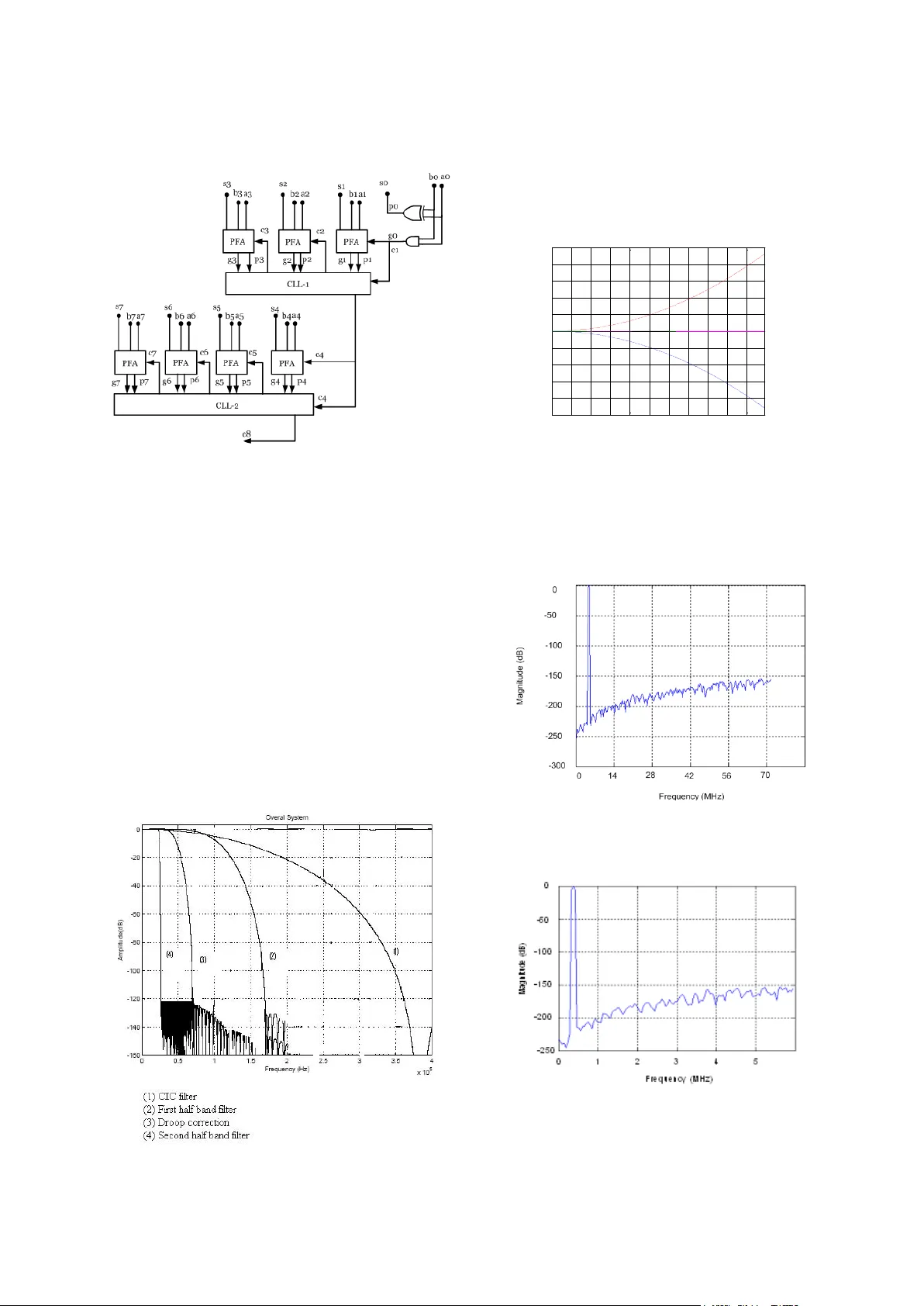
ICSE2006 Pro c. 2006, Kuala Lumpur, Mala ysia An Enhancement of Decimation Process using Fast Cascaded Integrator Comb (CIC) Filter Rozita Teym ourzadeh, IEEE Student Member, Masuri Bin Othm an VLSI Desig n Center, Institute of M icroengineering an d Nanoelectronic s (IMEN) Universiti K ebengsaan Malaysia, 43600 Bang i, Selangor, Malay sia rozita60 @vlsi.eng.ukm .my Abstract - The over sam pling technique has been shown to increase the SNR and is used in many high pe rformance syste m such as in the ADC for audio and DAT systems. This paper presents t he design of t he decimation and its VLSI implementation whi ch is t he sub- component in t he over sampling technique. The design of three main units in the decimation stage that is the Cascaded Integrator Comb (CIC) filter, the associated half band filters and the droop c orrection are also described. T he Verilog HDL code in Xilinx ISE environ ment has been derived to describe th e CIC filter properties and downloaded in t o Virt ex II FPGA board. In the design o f these un its, we focus on the trade-off between the speed improvemen t and the power consumption as well as the silicon area for the ch ip implementation. I. I NTRODUCTION The m ost popular A /D converters for audio applications are realized based on the use of over sam pling and sigma-delta ( ∑Δ) modulation techniques followed by decimation process [1]. Oversam pled Sigma delta (∑Δ) modulator provides high r esolution sa mple output in contrast to the standard Nyquist sampling technique. However at the output, the sampling process is needed in or der to bring down the hi gh sampling frequency and obtain high res olution. The CIC filter is a preferred technique f or this purpose. In 1981, Eugene Hog enauer [2 ] invented a new class of economical digita l filter for decim ation called a Cascaded I ntegrator Comb filt er (CI C) or rec ursiv e comb fil ter. This filter worked with sampling frequency of 5 MHz. Additionally t he CIC filter does not require storage for filter coefficients and multip liers as all coefficients ar e unity [3] . Furthermore its on - chip im plementation is effic ient becau se of its regular structure consisting of three basic building blocks, minim um external control and less complicated l ocal tim ing is required and its change factors is reconfig urable with the addition of a sc aling circuit and minimal changes to the filter timing . It is also used to perform filtering of the out of band quantization noise and prevent excess aliasing introduced during sampling rate decreasing. Hence enhanced high speed will be key issue in chip implem entation of CIC decimators. I n 1998, Garcia [4] designed Residue Number System (RNS) for pipelined Hog enauer CIC. C om pared to the two’s complement design, the RNS based Hogenaur filter enjoys an improved speed advanta ge by approximately 54%. Similar structure by Meyer -B aese [5] has been im plemented to reduce t he cost in the Hogenauer CIC filter wh ich shows that the filter can operate up to maxim um clock f requency of 164.1 MHz on Alte ra FPLD and 82.64 MHz on Synopsys cell- based IC design. This paper sh ows the implem entation of the high speed CI C filters which are consist of three parts, i ntegrator, comb and down sampler. The CIC filter is considered as recursive filter because of the f eedback loop i n integrator circuit and i t can work with m aximum throughput of 190 MHz. The next section describes the m athematical formulation and block diagram of CIC filters in detail. Enhanced high speed architecture is explained in section III . Section IV shows implem entation and design res ult in brief. Finally conclusion is expre ssed in section V. II. D EVELOPMENT OF A DECIMATION FILTER The purpose of the CI C filter is t wofo ld; firstly t o remove filtering noise which could be aliased back to th e bas e band si gnals and secondly to convert high sample rate m-bit data stream at the outpu t of the Sigm a-delta modulator to n -bit data stream with lower sample rate. This process is al so known as decimation which is essentially perfo rming t he averaging and a rate reduction functions simultaneously. ICSE2006 Pro c. 2006, Kuala Lumpur, Mala ysia Figure 1 shows th e decimation p rocess using CIC filter. Fig. 1 Digital Decimation P rocess The t wo half band filters [ 6] are used to reduce remain sam pling rate reduct ion to the Ny quist output rate. Fi rst half band filter and second half band filter mak e the frequency response more flat and sha rp similar to ideal filter frequency response. Droop correction filter is al located to compensate pass band attenuation w hich is created by the CIC filter. T he frequency response of overall system w ill be shown in section V. Table 1 shows filter specification in decimation proce ss. TABLE I F ILTER SPECI FICATIONS P ass band (kHz) Stop band (kHz) Transition band (kHz) CIC filter 7 384 377 First half band filter 32 170 138 Droop Correction 32 70 38 Second half band filter 21.77 26.53 4.76 II I. P RINCIPLE OF CIC FILTER STRUCTURE The CI C filter consi st of N stages of integrator and comb filter which are connected by a down sampler stage as shown in figure 1 in z domain. The CIC filter has the f ollowing transfer function: 1 0 ) ( ) 1 1 ( ) 1 ( ) ( ). ( ) ( RM k N k z N z N RM z z N C H z N I H z H (1 ) where N is the number of stage, M is the differential delay and R is the dec imation factor. In this paper, N, M a nd R have been chosen to be 5, 1 and 16 res pectively to avoid ov erflow in each stages. Fig. 2 One-stage of CIC filter block d iagram N, M and R are parameters to determ ine the register length requirem ents necessary to assure no data loss. Equation (1) ca n be express as follow: From the e quation, the maximum register growth/width, m a x G can be expre ssed a s: N RM G m ax (3) In other word, m ax G is the maxim um register growth and a f unction of the maximum output magnitude due to the worst possible input conditions [2]. If the input data word length is in B , most significant bit (MSB) at the filter output, m ax B is given by : ] 1 2 log [ max in B R N B (4) In order to reduce the data loss, normally t he first stage of the CI C fi lter has m aximum number of bit compared to the other stages. Since the integrator stage works at the highest oversampling rate wi th a l arge internal word length, decimation ratio and filter order incr ease which result in m ore power consumption and speed limitation. III. S P EED IMPROVEMENT A. Truncation for low power & high speed Truncation means estimating and removing Least Significant Bit (LSB) to reduce th e area requirements on chip and power consumption and also incre ase speed of calculation. Although N N RM k N RM k k N RM k k N RM k k N RM k k RM z z z z k h z H 1 0 1 0 1 0 1 0 ) 1 ( 0 1 ) ( ) ( (2) ICSE2006 Pro c. 2006, Kuala Lumpur, Mala ysia this estimation and removing introduces additional error, the error can be made small enough to be accept able for DSP appl ications. Figure 3 illustrates five stages of t he CIC filter when m ax B is 25 bit so truncati on is applied to reduce r egister width. Matlab software helps to find word length in integrator and comb section. Fig. 3 Five-stages of tr uncated CIC filter B. Pipeline structure One way to have high speed CI C f ilter is by implem enting the pipeline filt er structure. Figure 4 shows pipeline CIC filter structure when truncation is also applied. In the pipelined structure, no additi onal pipeline registers are used in integrator part. So that hardware requirement i s the same as in the n on-pipeline [7]. The CIC decimation filter clock rate is determined by the first integrator stage that causes more propag ation delay than any other stage due to maxim um number of bit. So it is possible to use a higher clock rate for a CI C decimation filter if a pipeli ne structure is used in the integrator s tages, as compared to non- pipelined integrator stages. The clock rate in integrator section is R times higher than in the comb section. Fig. 4 Five-stage o f truncated pipeline CIC filter Previously, the pipelin e structure for CIC fil ter was applied just for integrator part since the maximum clock rate is determined by the integrator. The abov e architecture show ed tha t the m axi mum throughput was increase d by 2 0 MHz when the pipeline structure is used for all the CI C parts consisting of integ rator, comb and down sampler. C. Modified Carry look-ahe ad Adder (MCLA) The other technique to increase speed is using Modified Carry Look- ahead Adder. The Carry Look-ahead adder (CLA) is the fastest adder which can be used for speeding up purpose but the disadvantage of the CLA adder is that the carry logic is getting quite com plicated for more than 4 b its so Mo dified Carry Look -ahead Adder (MCLA) is introduced to replace as adder. This improve in speed is due to the carry calculation in MCLA. In the ripple carry adder, most significant bit addition has to wait f or the carry to ripple through from t he least significant bit addition. Therefore the carry of MCLA adder has become a focus of study in speeding up the adder circuits [8]. The 8 bit MCLA structure is shown in Figure 5. Its block diagram consists o f 2, 4 -bit module which is connected and each previous 4 bit calculates carry out fo r the next carry . The CIC filt er in this paper has five MCLA i n integrator parts. The maxim u m number of bit is 25 and it i s decreased in next st ages. So it truncated respect ively to 25, 22, 20, 18 and 16 bit in each adder, left to right Notice that each 4-bit adder prov ides a group propagate and generate Signal, which is used by the MCLA Logic block. The group P ropagate P G and Generate G G of a 4 - bit adder will hav e the following expressions: 0 1 2 3 . . . p p p p P G (5) 0 1 2 3 1 2 3 2 3 3 . . . . . . g p p p g p p g p g G G (6) The most i mpor tant equations t o obtain carry of each stage hav e been defined as be low: ) . ( 0 0 0 1 c p g c ( 7) ) . . ( ) . ( 0 0 1 0 1 1 2 c p p g p g c (8) ) . . ( ) . . ( ) . ( 0 . 0 1 2 0 1 2 1 2 2 3 c p p p g p p g p g c (9 ) ) . . . ( ) . . ( ) . ( 0 1 2 3 1 2 3 2 3 3 4 g p p p g p p g p g c ) . . . . ( 0 0 1 2 3 c p p p p Calculation of MCLA is based on above equations. 8-Bit MCLA Adder could be constructed continu ing along in the same logic pattern, with the MSB carry-out resulting from OR & AND gates. The Verilog code has been written to implement addition. The MCLA Verilog code was downloaded to the Xilinx (10) ICSE2006 Pro c. 2006, Kuala Lumpur, Mala ysia FPGA chip. From X ilinx ISE sy nthesize report, it was found minimum clock period is 3.7 01ns (Maximum Fre quency is 270 MHz). Fig. 5 The 8 bit MCL A structu re V. I MPLEMENTATION After the si gm a delta m odulator, the sampling rate must be reduced to 48 KHz w hich is t he Nyquist sampling rate. T his is carried out i n 4 - stages. T he first stage involves the reduction of the sampling frequency by the decimation factor of 16. This is done by the CIC filter. The rem aining 3 st ages in volve the reduc tion of the sampl ing f requ ency by the dec imatio n facto r of 2 o nly which are carried out by the fi rst half band, droop correctio n and the second half band res pectiv ely. Figu re 6 illust rate the freq uency respon se of the overal l decim ation filte r whe n the sampl ing f requen cy is 6.144 MHz. Fig. 6 The frequen cy response of ove rall decimati on filte r Figure 7 shows the Droop cor rection filter result. This filter design a low pas s filter with pass band having t he shape of i nverse the CIC filter frequency response. So it compensates amplitude dr oop cause of t he CIC filter and makes whole syst em frequency respon se flat. 0 0. 2 0.4 0.6 0.8 1 1.2 1. 4 1.6 1.8 2 x 10 4 -0.25 -0.2 -0.15 -0.1 -0.05 0 0.05 0.1 0.15 0.2 0.25 SINC , Droop C orre ct ion and First Half -band Fi lters Freq uency (H z ) Amplitude(dB) Fig. 7 : Droop Co rrection eff ect on frequency response Figure 8 shows the measured baseband output spectra before (Fig ure 8(a)) and after (Figure 8(b)) the decimation func tions. (a) ( b) Fig. 8 Sign al spectra (a) Output sigma delta modulato r SNR (b) Output CIC filter SNR ICSE2006 Pro c. 2006, Kuala Lumpur, Mala ysia The CI C filter Verilog code was written and simulated by Matlab software. The signa l to noise ratio is 141.56 dB in si gm a delt a modulator output and it is increased to 145.35 dB in the decimation stages. To improve the signal to noise ratio, word length of r ecursive CI C filter should be increased but the speed of filter calcul ation is also decreased. The chip layout on Vir tex II FPGA boar d has been shown in F igure 9. Fig. 9 The core lay out on F PGA board IV. C ONCLUSION Recur sive CI C filter s have been desig ned and inves tigate d. Enhanced high Speed CIC filte rs was obtain ed by three ways. Th e pipe line stru cture , using the modi fied carry look- ahead adde r (MCLA ) and t runca tion le ad us to h ave high speed CIC filte r with the max imum thro ughpu t of 1 90 MHz. The evalua tion indi cates that the pipelin ed CIC filter with MCLA adder is attra ctive due to high speed whe n both the decim ation ratio and filte r orde r are not high as state d in the Hog enau er Comb fil ter. Sinc e the first stage of the CIC filt er requi re maxim um word leng th and al so becau se of th e re cursiv e loop in its str uctur e, the reduction in powe r consum ption is limite d by the throug hput . Thus the trunca tion will reduce the power consum ption and the numb er of calcul ation. The powe r consum ption compu ted using CAD tools (Cade nce and Synopsy s) and 0.18 μ m Silterr a tech nology library g ives 3.5 mW pow e r consum ption at m aximum clock fr equen cy. R EFERENCE [1] T. Ritoniemi, E.Paj arre. S. In galsuo, T. Hus u, V. Eerola, and T . Sar amiiki, “ A Stereo Audio Sigma-delta AD- Converter”. I EEE J. Solid – state Circ., Vol.29, no. 12, pp.1514 -1523, Dec. (1994) . [2] E.B. Ho genauer, “ An Eco nomical Class of digital filters for Decimation and interpolation ” , IEEE Transactions on Acoustics, Speech, and Signal Prosessing , Vol. ASSP -29,pp.155 -162, April (1981). [3] S. Park, “ Principles of Sigma-delta Modulation for Analog- to -Digital Co nverters ” , Motorola Inc , APR8/D Rev.1, ( 1990). [4] A.Garcia, U. Meyer -Baese & F. Taylor, “ Pipelined Hogenauer CIC Filters Using Field- Programmable Logic a nd Residue Number System ” . Acoustics, Speec h an d S ignal processing IEEE International Conference ,Vol. 5, pp.3085 -3088 (1998). [5] U. Meyer-Baese, S. Rao, J. Ra mirez, & A. Ga rcia, “ Cost-effective Ho genauer Cascad ed Integrator Comb Decimator Filter Design for custom I Cs ” . IEE Electronic journal. Vol. 41 , no. 3, pp. 158- 160 (2005). [6] P. B. Brandt & A. B ruce. Wooley, “ A Low- Power, Area-Ef ficient Digital Filter for Decimation and Interp olation ”. IEEE Journ al of Solid-S tate Circuits , Vol. 29, no.6, June ( 1994 ). [7] Y. Djad i and T. A. Kwasniewski, C. Cha n and V. Szwarc, “A high throughput P rogrammable Decimation and Interpolat ion Filter ” , Proceedin g of Internationa l Co nference on Signal Processing Applications and Tech nology , p p.1743-1748 , (1994 ). [8] D. M. Ciletti, A dva nced Digital design with the Verilog HDL, Prentice Hall, Depart ment of Electrical and Co mputer Eng ineering U niversity of Colorado at Colo rado Springs, ( 2003 ). [9] S. M. Mortazavi, S. M. Fakhraie & O. Shoaei. “ A Co mparative St ydy and Design of Decimation Filter For high-Prec ision Audio Data Converters”, The 17 IEEE in ternational conference on microelectron ics. p p.139-143, (2005).
Original Paper
Loading high-quality paper...
Comments & Academic Discussion
Loading comments...
Leave a Comment