A programmable clock generator for automatic Quality Assurance of LOCx2
The upgrade of ATLAS Liquid Argon Calorimeter (LAr) Phase-1 trigger requires high-speed, low-latency data transmission to read out the Lar Trigger Digitizer Board (LTDB). A dual-channel transmitter ASIC LOCx2 have been designed and produced. In order…
Authors: Zhi-yue Wang, Tian-kuan Liu, Qi-jie Tang
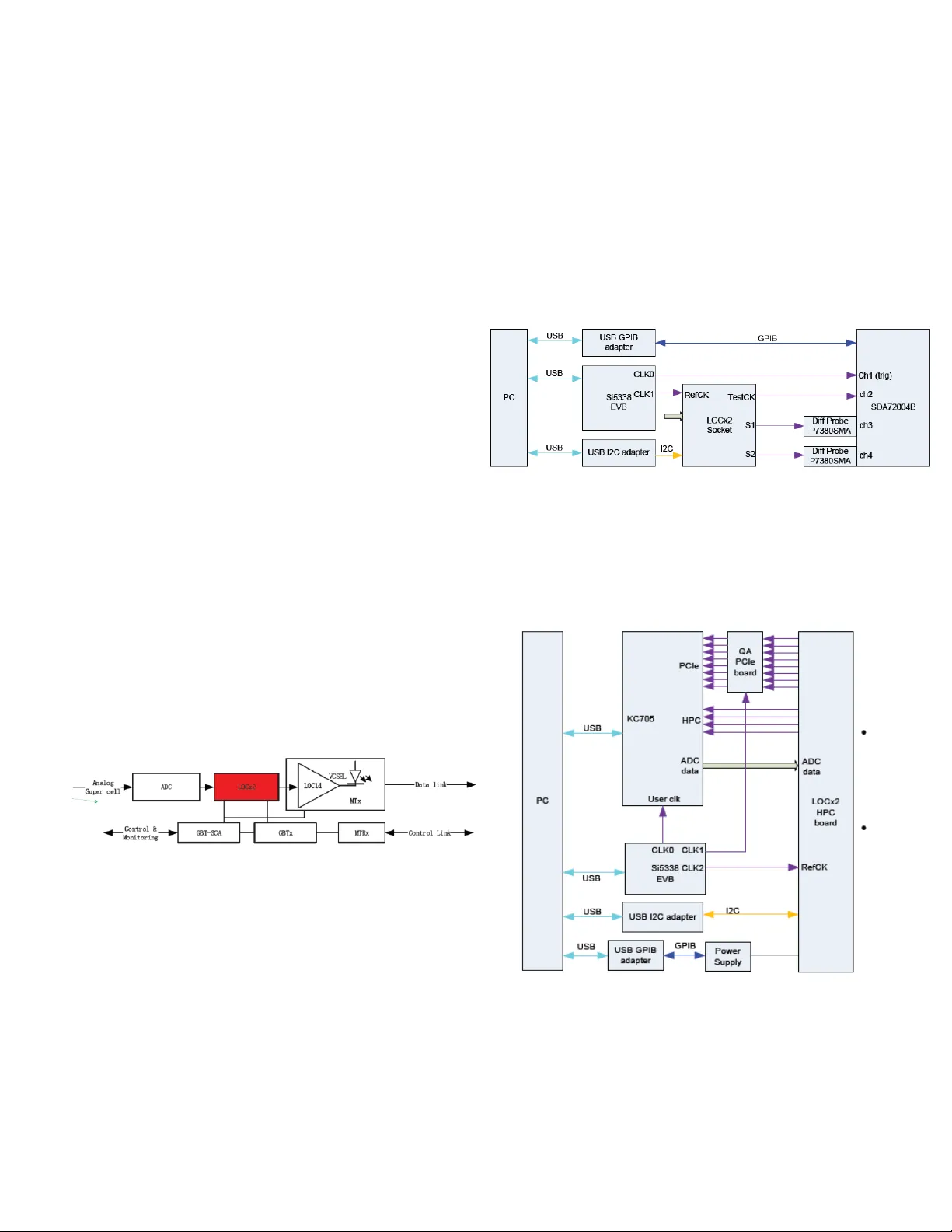
Zhi- yue Wang, Tian-kuan Liu, Qi -jie Tang, Yi Feng, Jian Wang, Senior M ember, IEEE Abstract – . The upgrade of ATLAS Liqu id Argon Calori meter (LAr) Phase-1 trigger requires high-speed, low-latency data transmission to read ou t the Lar Trigger Digitizer Board (LTDB). A dual-channel trans m itter ASIC LOCx2 have b een designed and produced. In order to ensure all the LOCx2 c hips behave properly, a Q uality Assurance n eeds to be conducted before assembly. The problem I was trying to solve in this project is to yield a clock signal w ith continuously adjustable fr equency a nd p hase offset to generate and control a n eye diagram for the QA. By configurin g the registers of a n any-frequency generator IC, Si53 38, th e cl ock signal w hose frequency range fr om 5MHz to 200 M Hz have been properly produced. For the purpose of further development, a C - language based DLL which packs u p the function of adjusting frequency and s etting phase offset w as designed and built, and several evaluation was performed to ensure the robustness of DL L. I. INTRODUCT ION The upgrade of AT LAS Liquid Argon Calori meter (LAr) made a demand o f a high -speed, low-latency data transmissio n to read out f rom the LAr T rigger Digtizer Board(LTDB ). In the LAr system, the detector was connected to th e front-End board, and a copy of r aw wave- form c ollect fro m detector pass through a linear m ixer and a L ayer Sum Bo ard (L SB). The output signal goes into the LTDB which split the signal into four ways of ADCs and the data yield by ADCs was caught by LOCx2, which was an ASIC d esigned to meet the requirement of high - speed and low-latency data tr ansmission. This part of syste m was shown in the Fig.1. Fig. 1. L ink system block diagram About 7000 LOCx2 were fabricated, therefore a Quality Assurance need to be done in or der to pick out those dies wi th better performance. The a mount of dies was too huge to perform a p ure artificial test one b y one, thus a n automatic test system was designed, which perform tests include eye diagram, Phase -Lock loop ,Bit Error Rate(BER), I2C and input sk e w. Fig.2. shows the Block This w ork was support ed by the National Natural Science Funds of China under G ran t No: 11603023, 11773 026, 1172850 9, the Fundamental R esea rch Funds for the C entral Unive rsities ( WK236000 0003, WK 2030040064), the Natural S cience F unds of A nhui Province u nder G rant No: 1508085MA07, the Research Funds of the State Key Laboratory of Parti cle Detection and Electronics, th e CA S Center for Exce llence in Part icle Physics, the Re search Funds of Key Laboratory o f Astronomical Optics & T echnology , CAS. diagram of LOCx2 eye diagram and PLL test setup. All 7000 LOCx2 chips will test the serial o utput eye diagram. About 1% of the ch ips that p ass th e eye d iagram tests and BER tests in each wafer will b e sampled to measure the Phase -Locked-loop (P LL) tuning range, the jitter o f the serial o utput. Fig.2 Block diagram o f LO Cx2 eye diagram and PL L test setup Fig.3 sho ws the Block diagram o f LOCx2 BER, I2C, and input skew test setup. All 7000 LOCx2 chips will get throu gh the test of BER and I2C. About 1% of the chips t hat pass the eye diagra m tests a nd BER tests in each wafer will be sampled to m ea sure the 3.125 -ns input sk ew tolerance in the ASIC ADC mode. Fig. 3. Block di agram of L OCx2 BER, I2C, and i nput skew te st setup The Authors Zhi-y ue Wang, Qi -jie Tang, Yi Feng, Jian Wang are with the State Key Laboratory of T echnolog ies of P article Detection and Electronics , University of Science a nd Technology o f C hina, Hefei, Anhui 230026, China (e -mail: Jian Wang, w angjian@ustc.edu.c n ). Tian-Kuan L iu is w ith the Departm ent of Phy sics, Sout hern Met hodist University, Dal las, TX 75275, USA , tliu@mail.sm u.edu A programmable clock generator for automatic Quality Assurance of LOCx2 As w as show n in these tw o diagrams, Si5338 play th e role of generating an any-frequenc y clock signal for test. A host PC will control and supervise t he whole test s ystem automaticall y. The signal yield ed by Si5338 w as feed to the LOCx2 and a SDA72004B(an oscillosco pe) simultaneously, and the o utput signal fro m LOCx2 together with the signal directl y transfer into SD A72004B yield an e ye diagram for test. And in t he BER test in order to shorte n t he time, a te st system which i s abl e to test 6 d ies s imultaneously was produced and in this s ystem, and the test signal was g enerated by KC705 which w as also f eed by Si5338, th erefore the Si5338 n eed to hav e the ability of adjusting the frequency of clock sig nal conti nuously with programming interface. A further test o f BER req uest an inp ut signal with a n alterab le pha se. All these fu nction need to b e provided by Si5338 EVB w hich does not provide a programming interface. So the m ain purpose o f t his work is to develop a set of Ap plication Programming Interface (API) in the P C side for further deve lopment and a MCU firmware to control the Si5338 to genera te up to four channels of any- frequency clock with controllable phase , which make it po ssible to control the entire s ystem with pro gramming auto matically. II. S TRUCTU RE OF SIGNAL GENERATIO N SYST EM HOST MCU : C 8051 F 340 Power Supp ly AD5263 + MAX 8869 Hardware SMBus Support USB Xpress : Slave MCU Firmwa re Signal Generation : Si5338 I2C BUS USB Xpress :Mast er USB Fig. 4.Block Diag ram of Si5338 EV B with host computer As was shown in Fig.4 , Si5338 is a programmable, any - frequency, four channel s clock sig nal ge nerator, whose out put signals ca n be configured by i ts registers, and t his is the kernel for generating th e cloc k sig nal s. C8051 F340 is a MCU based on CIP-51 cor e which m aintains the functio n of t he hardware SMBus I/O, and an USB-contro ller, which is used to communicate with SI5338 th rough I2C bus to configure the output of cloc k signal a nd the voltage of power supply m odules for Si5338 . AD5263 is a programmable variable resistor and MAX8869 is a voltage regulator . In o rder to meet the po wer supply f or five different VDD pins on the Si53 38, f ive c hannels of po wer supply module which co nsist o f a n AD5 263 and a MAX8869 were needed. AD5263 is co ntrolled by MCU through I2C bus as well. All these components were on the Si5338 EVB bo ard and make up the programmable clock generator. Concerning th e Si5338 EVB has a USB in terface, and C8051F340 MCU has a USB controller built-in, T he USB interface was c hoosen to se nd to and r eceive co mmands fr om MCU. A set of solutio n called USBXpress which could d rive the USB interface in both host and device was adop ted. Base on this software, we developed the host pro gram as well as de vice firmware which co mmunicate with each other through USB interface. III. T HE DESIG N OF DEVI C E FI RMWARE MCU C 8051 F 340 Configure A D 5263 Configure System Clock power sup plied? Load D efault Setting Phase O ffset Set Frequ ency Disable Output Enable O utput Receive packge from host Initiatio n SMBus Control ler USB Commu nication Parse & Send to I2C Read from I2 C & Pack Send back to host Fig. 5.Block Diag ram of MCU Firmw are The C8051F340 has a firmware no lar ger than 4352Bytes, which make it difficult to integrate a complex set of decis ion program into MCU firm ware after i mplemented the U SB communication. T herefore the firmware is desig ned to provide a communication bridge from I2C to USB, as w ell as configure all five c hannels of the power supply module. Therefore, the application on the hos t can just call a set o f routines which will send data ab out the device I2C address, register ad dress and t he value of register to device, and th e value will be written to ea ch register through I2C bus. Fig.5 sho ws the structure of fir mware, at the beginning of procedure, MCU would set u p the system clock, register the interrupt vectors, configure USB an d SMB controller and disable the har dware w atc h d og. Finished thi s basic start up routine, MCU would configure A D5263 and MAX88 69 through I2C bus to set u p the pow er supply for clock g enerator. After these procedure, MCU will enter a cir culation i n whi ch MCU would judge if a set of symbol variable were set, if so MCU will perform the procedure indicated by symbol variable. These symbol variable was set in the interrupt routi ne of USB . In the interrupt routine of USB which was trigged b y receiving command fro m U SB, device will firstly dete rmi ne what kind o f action was indicated b y this co mmand, read o r write, b y chec king the first b yte of co mmand, as 0xFF represent write while 0x00 repr esent read. If a ‘ w r ite ’ action w as to be performed, device will receive four bytes including the bytes of read or w rite. T he second by te is the hard ware I2C address of target device, the third byte is the ad dress of register in target device, and the last byte is the value to write. In the USB int errupt routine, these t hree bytes will be record into three di fferent variables, and FLA G_WRIT E, the s ymbol variab le would be set to 0 xFF and the interrupt routine wo uld finish. Back to mai n routine, progra m will ca tch this variable and w rite the a ddress and val ue to the register SM B0DAT, follo wed b y latc hing t he bit5 of SMB0CN. MC U will enter the SMB interrupt i n no longer than five ti mes cl ock period after this procedure and p erform a I2C writ ing. Aft er returning to mai n pr ocess, the s ymbol variable w ill be clear ed to 0x00. The whole process was shown i n Fi g.6 USB interr upt Reco rd Val ue and Addr ess FLAG_ WRIT E = 0xFF Writ e addr ess to SMB0D AT Main Proce ss SMB0C N | = 0x 10 Rece ive A comman d FLAG_ WRIT E = 0x 00 Fig.6. A W rite Proccess using I 2C interface Similarly, if a ‘ read ’ action was to be performed, device will record the address of register to read, set the correlated symbol variable, an d perform I2 C reading . The dif ferent is that a fter all the process have been done, MCU will write the value of register back to host t hrough USB. T he read process w as shown in Fig.7. USB interr upt Reco rd Val ue and Addr ess FLAG_ READ = 0xFF Writ e addr ess to SMB0D AT Main Proce ss SMB0C N | = 0x 10 Rece ive A com mand FLAG_ READ = 0x 00 Send Value To Ho st Fig.7.An Read Pr ocess using I 2C interface Since all the operation to Si5338 can be done by configuring the register th rough I2C bus, the function of fir mware can be regard as simple as a USB to I2C adapter. IV. T HE D ESIGH OF H OST S OFTWARE We try to decouple the host software into 4 lay er, as sho wn in Fig.8, the funda mental la yer drives the USB interface, and provide API for upper layer to read and w rite thro ugh USB. The second layer will pack up the protocol of command, which make it less co mplicated to instruct MCU. The third layer is th e most important one, as all the conf igure processes were done in this layer, it calls the A PI provided by fundamental layer, and provide several API, including modi fyin g the frequency of output clo ck signal, changing the phase a nd latchi ng ea ch channel of output. T he third layer, application la yer, is the user program which calls the API of second layer. Fig.8. L ayers of host softw are The first la yer mostly base on USBXpress, t hus we ca n handle USB interface by calling a set of high-level API w ithout dealing with USB protocol or develop ing system driver for USB by ourselve s. The USB Xpress provides a set of APIs , including SI_Op en for estab lishing the USB co mmunication, SI_Read for r eading data from USB interface, SI_Write for writing d ata to USB interface, and USB _Clos e for ter minating the USB communicatio n. USB2I2C.dll packs up these function in to three APIs, each handle the read, w rite and ini tiation. When an y of these APIs was called, USB2 I2C.dll w ould call the interface o f USBXpr ess and write command following t he p rotocol mentioned in the previous section, and i ndicate the MCU to perfor m I2C read and write. It p rovides three in terface, each handle the function of reading a value from a ce rtain register, writing a value to a certain register, and initiation. T his layer plays the role of middleware. LIB5338.dll calls the API provided b y USB2I2 C.dll to configure the re gisters of Si5338, so as to change t he frequency of output signals, adjust the phase offset, enable or disable a certain channel’s o utput, and pac k the se function up to sever al APIs. V. CONCLU SION We achieved the goal of generating an any-frequenc y sig nal and control t he it s phase offset, and we d evelop this set of software for both host PC a nd MCU, and the entire system works p roperly. Now t he device ha ve p layed its role in the whole testing system. VI. R EFERENCES [1] SILICON , L. "USB Xpress Pr ogrammer ’s Guide." (2007). [2] Xiao, L., et al. "L OCx2, a low-l atency, l ow-ov erhead, 2× 5 .12 -Gb ps transmitter ASIC for the A TLAS Liquid Argon Calorimeter trigger upgrade." Jour nal of Instrumenta tion 11.02 (2016): C02013.
Original Paper
Loading high-quality paper...
Comments & Academic Discussion
Loading comments...
Leave a Comment