Tiered-Latency DRAM: Enabling Low-Latency Main Memory at Low Cost
This paper summarizes the idea of Tiered-Latency DRAM (TL-DRAM), which was published in HPCA 2013, and examines the work’s significance and future potential. The capacity and cost-per-bit of DRAM have historically scaled to satisfy the needs of increasingly large and complex computer systems. However, DRAM latency has remained almost constant, making memory latency the performance bottleneck in today’s systems. We observe that the high access latency is not intrinsic to DRAM, but a trade-off is made to decrease the cost per bit. To mitigate the high area overhead of DRAM sensing structures, commodity DRAMs connect many DRAM cells to each sense amplifier through a wire called a bitline. These bit-lines have a high parasitic capacitance due to their long length, and this bitline capacitance is the dominant source of DRAM latency. Specialized low-latency DRAMs use shorter bitlines with fewer cells, but have a higher cost-per-bit due to greater sense amplifier area overhead. To achieve both low latency and low cost per bit, we introduce Tiered-Latency DRAM (TL-DRAM). In TL-DRAM, each long bitline is split into two shorter segments by an isolation transistor, allowing one of the two segments to be accessed with the latency of a short-bitline DRAM without incurring a high cost per bit. We propose mechanisms that use the low-latency segment as a hardware-managed or software-managed cache. Our evaluations show that our proposed mechanisms improve both performance and energy efficiency for both single-core and multiprogrammed workloads. Tiered-Latency DRAM has inspired several other works on reducing DRAM latency with little to no architectural modification.
💡 Research Summary
The paper introduces Tiered‑Latency DRAM (TL‑DRAM), a novel DRAM architecture that simultaneously reduces access latency and preserves the low cost‑per‑bit of conventional commodity DRAM. The authors begin by highlighting the long‑standing problem that DRAM capacity and cost have scaled dramatically over the past decade, yet the fundamental timing parameters (tRCD, tRC) have improved only modestly, leaving memory latency as a dominant performance bottleneck for modern processors.
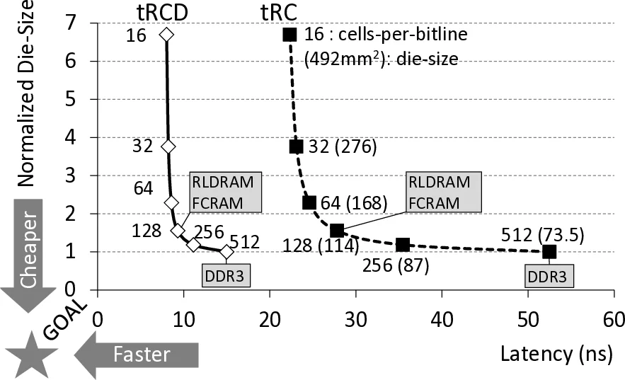
Through detailed analysis, they identify the parasitic capacitance of long bitlines as the primary source of this latency. Long bitlines connect many cells to a single sense amplifier, which amortizes the large area of the amplifier but incurs a large electrical load. Shortening the bitline reduces capacitance and thus latency, but requires many more sense amplifiers, inflating die area and cost. Existing low‑latency DRAMs (e.g., RLDRAM, FCRAM) adopt the short‑bitline approach at the expense of a substantial cost increase.
TL‑DRAM resolves this trade‑off by inserting an isolation transistor midway along each bitline, thereby partitioning the line into a “near” segment (directly attached to the sense amplifier) and a “far” segment (connected through the transistor). When accessing a cell in the near segment, the transistor is turned off, effectively shortening the bitline and achieving latency comparable to a short‑bitline design. When accessing the far segment, the transistor is turned on, re‑establishing the full‑length bitline; however, the transistor’s resistance slows voltage propagation, increasing the far‑segment latency. Circuit‑level SPICE simulations (based on a 55 nm DDR3 process) show that a near segment of 128 cells (≈25 % of a 512‑cell bitline) yields tRCD and tRC of roughly 4 ns and 23 ns, respectively—about half the latency of an unsegmented long bitline. The far segment’s latency rises to ~66 ns, but the overall die‑area overhead is only ~3 % because only the isolation transistors are added.
The paper proposes two families of mechanisms to exploit the asymmetric latency. The first treats the near segment as a hardware‑managed cache for the far segment. Three cache‑replacement policies are evaluated, and a novel “inter‑segment data transfer” operation moves an entire row from far to near (or vice‑versa) over the shared bitline in ~4 ns without using the external memory channel, allowing other banks to be accessed concurrently. The second approach exposes the near segment to the operating system, enabling page‑level placement of frequently accessed pages into the low‑latency region via static or dynamic profiling. Both approaches dramatically increase the hit rate in the near segment (over 90 % in the authors’ workloads), leading to substantial performance and energy gains.
Evaluation using the open‑source Ramulator DRAM simulator integrated with an in‑house processor model shows average IPC improvements of 12.8 % (single‑core), 12.3 % (dual‑core), and 11.0 % (four‑core) over a baseline DDR3 system. Power consumption drops by 23.6 %–28.6 % across the same configurations, primarily because near‑segment accesses consume roughly half the energy of conventional accesses, while far‑segment accesses consume more but are infrequent.
Beyond the immediate benefits, TL‑DRAM has inspired a line of subsequent research that leverages intra‑DRAM data movement (e.g., RowClone, LISA, DARP) and explores new memory‑controller policies, confirming the broad impact of the tiered‑latency concept. In conclusion, TL‑DRAM demonstrates that by modestly augmenting the DRAM bitline with an isolation transistor, designers can achieve near‑short‑bitline latency for a fraction of the cells while retaining the cost efficiency of long‑bitline DRAM, offering a practical path to mitigate the memory‑latency wall in current and future computing systems.
Comments & Academic Discussion
Loading comments...
Leave a Comment